STPS50U100C
Ultralow forward voltage power Schottky rectifier
Features
A1
■ ■ ■ ■
Ultralow forward voltage drop High current capability High frequency operation ECOPACK®2 compliant components
K A2
A2
Description
The STPS50U100C is a dual power Schottky diode rectifier, suited for high frequency switch mode power supply. Featuring an ultralow forward voltage drop, this device, packaged in TO-220AB and I²PAK, is intended to be used in notebook, game station and desktop adaptors as well as server SMPS. It has been especially designed to help power supply manufacturers meet the recently introduced worldwide efficiency standards.
A1
K A1
K
A2
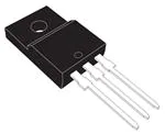
TO-220AB STPS50U100CT
I2PAK STPS50U100CR
Table 1.
Device summary
Symbol IF(AV) VRRM Value 2 x 25 A 100 V 0.64 V 150 °C
VF(TYP) @ 25 A @ 125 °C Tj (max)
November 2009
Doc ID 16603 Rev 1
1/8
www.st.com 8
�Characteristics
STPS50U100C
1
Table 2.
Symbol VRRM IF(RMS) IF(AV) IFSM Tstg Tj
1.
Characteristics
Absolute ratings (limiting values per diode at 25 °C, unless otherwise specified)
Parameter Repetitive peak reverse voltage Forward rms current Average forward current, δ = 0.5 Surge non repetitive forward current Storage temperature range Maximum operating junction temperature(1) TC = 120 °C Per diode TC = 105 °C Per device tp = 10 ms, half sine-wave Value 100 50 25 50 250 -65 to + 150 150 Unit V A A A °C °C
1 dPtot < condition to avoid thermal runaway for a diode on its own heatsink Rth(j-a) dTj
Table 3.
Symbol Rth (j-c) Rth (c)
Thermal resistance
Parameter Junction to case Coupling Per diode Per device Value 1.3 0.9 0.45 Unit °C/W °C/W
When the diodes 1 and 2 are used simultaneously: ΔTj(diode 1) = P(diode1) x Rth(j-c)(Per diode) + P(diode 2) x Rth(c) Table 4.
Symbol
Static electrical characteristics
Parameter Tests conditions Tj = 25 °C VR = 70 V Min. VR = VRRM IF = 5 A IF = 15 A IF = 25 A Typ. 15 10 30 15 0.48 0.38 0.58 0.54 0.67 0.64 Max. 200 40 V 0.73 0.7 Unit µA mA µA mA
IR
Reverse leakage current
Tj = 125 °C Tj = 25 °C Tj = 125 °C Tj = 25 °C Tj = 125 °C
VF
Forward voltage drop
Tj = 25 °C Tj = 125 °C Tj = 25 °C Tj = 125 °C
To evaluate the conduction losses use the following equation: P = 0.475 x IF(AV) + 0.009 IF2(RMS)
2/8
Doc ID 16603 Rev 1
�STPS50U100C
Characteristics
Figure 1.
Average forward power dissipation Figure 2. versus average forward current (per diode)
250
Non repetitive surge peak forward current versus overload duration (maximum values, per diode)
28 24 20 16 12 8
PF(AV)(W)
δ = 0.05 δ = 0.1 δ = 0.2 δ = 0.5
IM(A)
δ=1
225 200 175 150 125 100 75
Tc = 25 °C Tc = 75 °C Tc = 125 °C t δ = 0.5
1.E-02 1.E-01
T
50 25
4
δ = tp / T
IM
0 0 5 10 15 20
tp
25
IF(AV)(A)
30 35
0 1.E-03
t(s)
1.E+00
Figure 3.
Reverse leakage current versus reverse voltage applied (typical values, per diode)
Tj = 150 °C
Figure 4.
Average forward current versus ambient temperature (δ = 0.5, per diode)
Rth(j-a) = Rth(j-c)
1.E+02
IR(mA)
30 25 20 15 10
IF(AV)(A)
1.E+01
Tj = 125 °C Tj = 100 °C
1.E+00 Tj = 75 °C 1.E-01 Tj = 50 °C Tj = 25 °C 5
1.E-02
T δ = tp / T
1.E-03 0 10 20 30 40 50 60 70 80
VR(V)
0 90 100 0
tp
25 50 75
Tamb(°C)
100 125 150
Figure 5.
Relative variation of thermal Figure 6. impedance junction to case versus pulse duration
10000
Junction capacitance versus reverse voltage applied (typical values, per diode)
F = 1 MHz Vosc = 30 mVRMS Tj = 25 °C
1.0 0.9 0.8 0.7 0.6 0.5 0.4 0.3 0.2 0.1
Zth(j-c)/Rth(j-c)
C(pF)
1000
Single pulse
0.0 1.E-04
tp(s)
1.E-03 1.E-02 1.E-01 1.E+00 100 1 10
VR(V)
100
Doc ID 16603 Rev 1
3/8
�Application information Figure 7. Forward voltage drop versus forward current (per diode)
50 45 40 35 30 25 20 15 10 5 0 0.0 0.1 0.2 0.3 0.4 0.5 0.6 0.7 0.8
STPS50U100C
IFM(A)
Tj = 125 °C (Maximum value)
Tj = 125 °C (Typical value)
Tj = 25 °C (Maximum value)
VFM(V)
0.9 1.0
2
Application information
It is mandatory to ensure a peak reverse voltage below the VRRM absolute rating. Therefore, it is recommended to use a RC clamping snubber circuit in parallel with the STPS50U100C device. Figure 8. Application schematic
R
C
DC/DC input
DC/DC output
STPS50U100C
4/8
Doc ID 16603 Rev 1
�STPS50U100C
Package information
3
Package information
● ● ●
Epoxy meets UL94,V0 Cooling method: by conduction (C) Recommended torque value: 0.4 to 0.6 N·m
In order to meet environmental requirements, ST offers these devices in different grades of ECOPACK® packages, depending on their level of environmental compliance. ECOPACK® specifications, grade definitions and product status are available at: www.st.com. ECOPACK® is an ST trademark. Table 5. TO-220AB dimensions
Dimensions Ref. Millimeters Min. A C
H2 Dia L5 L7 L6 L2 F2 F1 L9 L4 F G1 G M E D C A
Inches Min. 0.173 0.048 0.094 0.019 0.024 0.044 0.044 0.194 0.094 0.393 Max. 0.181 0.051 0.107 0.027 0.034 0.066 0.066 0.202 0.106 0.409
Max. 4.60 1.32 2.72 0.70 0.88 1.70 1.70 5.15 2.70 10.40
4.40 1.23 2.40 0.49 0.61 1.14 1.14 4.95 2.40 10
D E F F1 F2 G G1 H2 L2 L4 L5 L6 L7 L9 M Diam.
16.4 typ. 13 2.65 15.25 6.20 3.50 14 2.95 15.75 6.60 3.93
0.645 typ. 0.511 0.104 0.600 0.244 0.137 0.551 0.116 0.620 0.259 0.154
2.6 typ. 3.75 3.85
0.102 typ. 0.147 0.151
Doc ID 16603 Rev 1
5/8
�Package information Table 6. I2PAK dimensions
STPS50U100C
Dimensions Ref. Millimeters Min.
A E L2 c2
Inches Min. 0.173 0.094 0.024 0.044 0.019 0.048 0.352 0.094 0.195 0.394 0.512 0.138 0.050 Max. 0.181 0.107 0.035 0.067 0.028 0.052 0.368 0.106 0.203 0.409 0.551 0.155 0.055
Max. 4.60 2.72 0.88 1.70 0.70 1.32 9.35 2.70 5.15 10.40 14 3.93 1.40
A A1 b b1
4.40 2.40 0.61 1.14 0.49 1.23 8.95 2.40 4.95 10 13 3.50 1.27
D
c c2
L1 L b1
A1
D e e1 E
b e e1
c
L L1 L2
6/8
Doc ID 16603 Rev 1
�STPS50U100C
Ordering information
4
Ordering information
Table 7. Ordering information
Marking STPS50U100C STPS50U100C Package TO-220AB I PAK
2
Order code STPS50U100CT STPS50U100CR
Weight 2.23 g 1.49 g
Base qty 50 50
Delivery mode Tube Tube
5
Revision history
Table 8.
Date 17-Nov-2009
Document revision history
Revision 1 First release. Changes
Doc ID 16603 Rev 1
7/8
�STPS50U100C
Please Read Carefully:
Information in this document is provided solely in connection with ST products. STMicroelectronics NV and its subsidiaries (“ST”) reserve the right to make changes, corrections, modifications or improvements, to this document, and the products and services described herein at any time, without notice. All ST products are sold pursuant to ST’s terms and conditions of sale. Purchasers are solely responsible for the choice, selection and use of the ST products and services described herein, and ST assumes no liability whatsoever relating to the choice, selection or use of the ST products and services described herein. No license, express or implied, by estoppel or otherwise, to any intellectual property rights is granted under this document. If any part of this document refers to any third party products or services it shall not be deemed a license grant by ST for the use of such third party products or services, or any intellectual property contained therein or considered as a warranty covering the use in any manner whatsoever of such third party products or services or any intellectual property contained therein.
UNLESS OTHERWISE SET FORTH IN ST’S TERMS AND CONDITIONS OF SALE ST DISCLAIMS ANY EXPRESS OR IMPLIED WARRANTY WITH RESPECT TO THE USE AND/OR SALE OF ST PRODUCTS INCLUDING WITHOUT LIMITATION IMPLIED WARRANTIES OF MERCHANTABILITY, FITNESS FOR A PARTICULAR PURPOSE (AND THEIR EQUIVALENTS UNDER THE LAWS OF ANY JURISDICTION), OR INFRINGEMENT OF ANY PATENT, COPYRIGHT OR OTHER INTELLECTUAL PROPERTY RIGHT. UNLESS EXPRESSLY APPROVED IN WRITING BY AN AUTHORIZED ST REPRESENTATIVE, ST PRODUCTS ARE NOT RECOMMENDED, AUTHORIZED OR WARRANTED FOR USE IN MILITARY, AIR CRAFT, SPACE, LIFE SAVING, OR LIFE SUSTAINING APPLICATIONS, NOR IN PRODUCTS OR SYSTEMS WHERE FAILURE OR MALFUNCTION MAY RESULT IN PERSONAL INJURY, DEATH, OR SEVERE PROPERTY OR ENVIRONMENTAL DAMAGE. ST PRODUCTS WHICH ARE NOT SPECIFIED AS "AUTOMOTIVE GRADE" MAY ONLY BE USED IN AUTOMOTIVE APPLICATIONS AT USER’S OWN RISK.
Resale of ST products with provisions different from the statements and/or technical features set forth in this document shall immediately void any warranty granted by ST for the ST product or service described herein and shall not create or extend in any manner whatsoever, any liability of ST.
ST and the ST logo are trademarks or registered trademarks of ST in various countries. Information in this document supersedes and replaces all information previously supplied. The ST logo is a registered trademark of STMicroelectronics. All other names are the property of their respective owners.
© 2009 STMicroelectronics - All rights reserved STMicroelectronics group of companies Australia - Belgium - Brazil - Canada - China - Czech Republic - Finland - France - Germany - Hong Kong - India - Israel - Italy - Japan Malaysia - Malta - Morocco - Philippines - Singapore - Spain - Sweden - Switzerland - United Kingdom - United States of America www.st.com
8/8
Doc ID 16603 Rev 1
�
很抱歉,暂时无法提供与“STPS50U100CT”相匹配的价格&库存,您可以联系我们找货
免费人工找货