TN2015H-6I
Datasheet
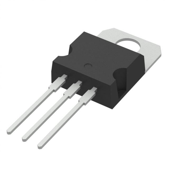
20 A 600 V high temperature SCR thyristors in insulated TO-220
Features
A
G
K
K
A
•
High junction temperature: Tj max. = 150 °C
•
•
High static immunity dV/dt = 750 V/µs up to 150 °C
Peak off-state voltage VDRM/VRRM = 600 V
•
•
High turn-on current rise dI/dt = 100 A/µs
Insulated package TO-220AB:
–
Insulated voltage: 2500 VRMS
•
•
G
–
Complies with UL 1557 (File ref : E81734)
ECOPACK2 compliant
Halogen-free molding, lead-free plating
TO-220AB insulated
Applications
•
•
•
•
General purpose AC line load switching
Motor control circuits and starters
Inrush current limiting circuits
Heating resistor control, solid state relays
Description
Thanks to its operating junction temperature up to 150°C, the TN2015H-6I offers high
thermal performance operation up to 20 A rms.
Product status
TN2015H-6I
Product summary
Order code
TN2015H-6I
Package
TO-220AB Ins.
IT(RMS)
20 A
VDRM/VRRM
600 V
Tj max.
150 °C
Its trade-off noise immunity (dV/dt = 750 V/μs) versus its gate triggering current
(IGT = 15 mA) and its turn-on current rise (dI/dt = 100 A/μs) allows to design robust
and compact control circuit for voltage regulator in motorbikes and industrial drives,
overvoltage crowbar protection, motor control circuits in power tools and kitchen
appliances and inrush current limiting circuits.
DS13203 - Rev 1 - December 2019
For further information contact your local STMicroelectronics sales office.
www.st.com
�TN2015H-6I
Characteristics
1
Characteristics
Table 1. Absolute maximum ratings (limiting values), Tj = 25 °C unless otherwise specified
Symbol
Parameter
Value
Unit
Tc = 113 °C
20
A
Tc = 112 °C
13
Tc = 130 °C
8
Tc = 139 °C
5
tp = 8.3 ms
197
tp = 10 ms
180
tp = 10 ms
162
A2s
f = 60 Hz
100
A/µs
600
V
tp = 10 ms
VDRM/VRRM + 100 V
V
Tj = 150 °C
4
A
Tj = 150 °C
1
W
5
V
Storage junction temperature range
-40 to +150
°C
Tj
Maximum operating junction temperature
-40 to +150
°C
Tl
Maximum lead temperature soldering during 10 s
260
°C
Insulation rms voltage, 1 minute
2500
V
IT(RMS)
RMS on-state current (180 ° conduction angle)
IT(AV)
Average on-state current (180 ° conduction angle)
ITSM
Non repetitive surge peak on-state current (Tj initial = 25 °C)
I2t value for fusing, (Tj initial = 25 °C)
I2t
IG = 2 x IGT, tr ≤ 100 ns
dl/dt
Critical rate of rise of on-state current
VDRM/VRRM
Repetitive peak off-state voltage
VDSM/VRSM
Non Repetitive peak off-state voltage
IGM
Peak gate current
PG(AV)
Average gate power dissipation
VRGM
Maximum peak reverse voltage
Tstg
Viso
tp = 20 µs
A
A
Table 2. Electrical characteristics (Tj = 25 °C unless otherwise specified)
Symbol
IGT
Test conditions
Value
VD = 12 V, RL = 33 Ω
VGT
DS13203 - Rev 1
Typ.
6
Max.
15
Max.
1.3
V
Min.
0.1
V
mA
VGD
VD = VDRM, RL = 3.3 kΩ
IH
IT = 500 mA, gate open
Max.
50
mA
IL
IG = 1.2 x IGT
Max.
60
mA
Min.
750
V/µs
Typ.
1.9
µs
Typ.
70
µs
dV/dt
VD = 402 V, gate open
tgt
IT = 40 A, VD = 402 V, IG = 20 mA, (dIG/dt) max = 0.2 A/µs
tq
IT = 20 A, VD = 402 V, (dIG/dt) max = 30 A/µs, VR = 25 V, dVD/dt = 40 V/µs
Tj = 150 °C
Unit
Tj = 150 °C
Tj = 150 °C
page 2/10
�TN2015H-6I
Characteristics
Table 3. Static characteristics
Symbol
Test conditions
Value
Unit
VTM
ITM = 40 A, tp = 380 µs
Tj = 25 °C
Max.
1.60
VTO
Threshold voltage
Tj = 150 °C
Max.
0.82
RD
Dynamic resistance
Tj = 150 °C
Max.
17.5
mΩ
5
µA
2
mA
IDRM, IRRM
Tj = 25 °C
VD = VDRM; VR = VRRM
Max.
Tj = 150 °C
V
Table 4. Thermal parameters
Symbol
DS13203 - Rev 1
Parameter
Value
Rth(j-c)
Junction to case (DC)
Max.
2.1
Rth(j-a)
Junction to ambient (DC)
Typ.
60
Unit
°C/W
page 3/10
�TN2015H-6I
Characteristics (curves)
1.1
Characteristics curves
Figure 1. Maximum power dissipation versus average onstate current
20
Figure 2. Average and DC on-state current versus case
temperature
P(W)
IT(AV) (A)
22
18
α = 120 °
16
α = 180 °
DC
18
α = 90 °
14
α = 90°
16
α = 60 °
14
α = 30 °
12
DC
20
α = 120°
α = 180°
α = 60°
α = 30°
12
10
10
8
8
6
6
360 °
4
2
4
2
IT(AV) (A)
α
0
2
4
6
8
10
12
14
Tc(°C)
0
0
16
Figure 3. Average and D.C. on state current versus
ambient temperature
0
1.0E+00
2
75
100
125
150
K = [Zth/ Rth]
Zth(j-c)
DC
2.5
50
Figure 4. Relative variation of thermal impedance junction
to case and junction to ambient versus pulse duration
IT(AV) (A)
3
25
Zth(j-a)
α = 180 °
1.5
1.0E-01
1
0.5
tP(s)
Ta(°C)
0
0
25
50
75
1.0E-02
100
125
150
Figure 5. Relative variation of gate triggering current and
gate voltage versus junction temperature (typical values)
IGT, VGT [ Tj ] / IGT, VGT [ Tj = 25 °C]
I
1.0E-02
1.0E+00
1.0E+01
1.0E+02
1.0E+03
IH, IL [ Tj ] / IH, IL [ Tj = 25 °C]
2.0
GT
1.0E-01
Figure 6. Relative variation of holding and latching
current versus junction temperature (typical values)
2.4
2.5
2.0
1.0E-03
I
H
1.6
1.5
1.2
1.0
VGT
0.8
0.5
0.0
-50
IL
0.4
Tj(°C)
Tj(°C)
-25
DS13203 - Rev 1
0
25
50
75
100
125
150
0.0
-50
-25
0
25
50
75
100
125
150
page 4/10
�TN2015H-6I
Characteristics (curves)
Figure 7. Relative variation of static dV/dt immunity
versus junction temperature
12
Figure 8. Surge peak on-state current versus number of
cycles
I
dV/dt [Tj] / dV/dt [Tj= 150 °C]
200 TSM
(A)
Non repetitive Tj = 25 °C
Above test equipment capability
tp=10ms
150
One cycle
8
100
4
VD = VR = 402 V
50
Tj (°C)
0
25
50
75
Number of cycles
100
125
0
150
Figure 9. Non repetitive surge peak on-state current for a
sinusoidal pulse with width tp < 10 ms
10000
Repetitive Tc = 113 °C
ITSM(A)
1
10
100
1000
Figure 10. On-state characteristics (maximum values)
ITM(A)
1000
Tj initial = 25 °C
100
1000
Tj max:
Vt0 = 0.82 V
Rd = 17.5 mΩ
ITSM
dl/dt limitation: 100 A/µs
10
100
Tj = 150 °C
10
0.01
tp(ms)
0.1
1
Tj = 25 °C
VTM(V)
1
0
10
0.5
1
1.5
2
2.5
3
3.5
4
Figure 11. Relative variation of leakage current versus junction
IDRM, IRRM [ Tj ; VDRM, VRRM ] / IDRM , IRRM [ 150 °C; 600 V ]
1.E+00
VDRM = VRRM = 600 V
1.E-01
1.E-02
1.E-03
Tj(°C)
1.E-04
25
DS13203 - Rev 1
50
75
100
125
150
page 5/10
�TN2015H-6I
Package information
2
Package information
In order to meet environmental requirements, ST offers these devices in different grades of ECOPACK packages,
depending on their level of environmental compliance. ECOPACK specifications, grade definitions and product
status are available at: www.st.com. ECOPACK is an ST trademark.
2.1
TO-220AB insulated package information
•
•
•
•
Molding compound resin is halogen-free and meets flammability standard UL94 level 0
Lead-free package leads finishing
ECOPACK2 compliant
Recommended torque: 0.4 to 0.6 N.m
Figure 12. TO-220AB insulated package outline
C
B
b2
I
Resin gate 0.5 mm
max. protusion(1)
L
F
A
I4
l3
c2
a1
l2
a2
M
b1
e
Resin gate 0.5 mm
max. protusion(1)
c1
(1)Resin gate position accepted in one of the two positions or in the symmetrical opposites.
DS13203 - Rev 1
page 6/10
�TN2015H-6I
TO-220AB insulated package information
Table 5. TO-220AB insulated package mechanical data
Dimensions
Ref.
Min.
A
Inches(1)
Millimeters
Typ.
15.20
a1
Max.
Min.
15.90
0.5984
3.75
Typ.
Max.
0.6260
0.1476
a2
13.00
14.00
0.5118
0.5512
B
10.00
10.40
0.3937
0.4094
b1
0.61
0.88
0.0240
0.0346
b2
1.23
1.32
0.0484
0.0520
C
4.40
4.60
0.1732
0.1811
c1
0.49
0.70
0.0193
0.0276
c2
2.40
2.72
0.0945
0.1071
e
2.40
2.70
0.0945
0.1063
F
6.20
6.60
0.2441
0.2598
I
3.73
3.88
0.1469
0.1528
L
2.65
2.95
0.1043
0.1161
I2
1.14
1.70
0.0449
0.0669
I3
1.14
1.70
0.0449
0.0669
I4
15.80
16.80
0.6220
M
16.40
2.6
0.6457
0.6614
0.1024
1. Inch dimensions are for reference only.
DS13203 - Rev 1
page 7/10
�TN2015H-6I
Ordering information
3
Ordering information
Figure 13. Ordering information scheme
TN 20 15
H - 6
I
Series
TN = SCR
RMS current
20 = 20 A
Gate triggering current
15 = 15 mA
High temperature
H = 150 °C
Voltage
6 = 600 V
Package
I = TO-220AB insulated
Delivery mode
Blank = tube
Table 6. Ordering information
DS13203 - Rev 1
Order code
Marking
Package
Weight
Base qty.
Delivery mode
TN2015H-6I
TN2015H6I
TO-220AB Ins.
2.3 g
50
Tube
page 8/10
�TN2015H-6I
Revision history
Table 7. Document revision history
DS13203 - Rev 1
Date
Revision
16-Dec-2019
1
Changes
Initial release.
page 9/10
�TN2015H-6I
IMPORTANT NOTICE – PLEASE READ CAREFULLY
STMicroelectronics NV and its subsidiaries (“ST”) reserve the right to make changes, corrections, enhancements, modifications, and improvements to ST
products and/or to this document at any time without notice. Purchasers should obtain the latest relevant information on ST products before placing orders. ST
products are sold pursuant to ST’s terms and conditions of sale in place at the time of order acknowledgement.
Purchasers are solely responsible for the choice, selection, and use of ST products and ST assumes no liability for application assistance or the design of
Purchasers’ products.
No license, express or implied, to any intellectual property right is granted by ST herein.
Resale of ST products with provisions different from the information set forth herein shall void any warranty granted by ST for such product.
ST and the ST logo are trademarks of ST. For additional information about ST trademarks, please refer to www.st.com/trademarks. All other product or service
names are the property of their respective owners.
Information in this document supersedes and replaces information previously supplied in any prior versions of this document.
© 2019 STMicroelectronics – All rights reserved
DS13203 - Rev 1
page 10/10
�
很抱歉,暂时无法提供与“TN2015H-6I”相匹配的价格&库存,您可以联系我们找货
免费人工找货