TSV7721, TSV7722, TSV7723
Datasheet
High bandwidth (22 MHz) low offset (200 μV) 5 V op amp
Features
TSV7722
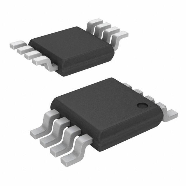
DFN8 2x2 mm
TSV7721
SOT23 -5
•
•
•
•
•
•
•
•
•
TSV7723
MiniSO10
TSV7722
MiniSO8
TSV7722
SO8
Gain bandwidth product 22 MHz, unity gain stable
High accuracy input offset voltage: 50 µV typ., 200 µV max.
Low input bias current: 2 pA typ.
Low input voltage noise density: 7 nV/√Hz
Wide supply voltage range: 1.8 V to 5.5 V
Output rail-to-rail
Input common-mode range includes low rail
Automotive grade and shutdown versions available
Benefits:
–
High frequency signal conditioning
–
Optimized accuracy for low-side current sensing
Applications
•
•
•
•
Low-side current measurement
Photodiode amplifiers
Automotive current measurement and sensor signal conditioning
Strain gauges signal conditioning
TSV7721
TSV7722
TSV7723
Automotive
Maturity
status link
Channel
Description
1
1
Package
SOT23-5
•
SOT23-5
2
DFN8
2
MiniSO8
2
SO8
2
•
MiniSO8
2
•
SO8
2
The TSV7721, TSV7722 and TSV7723 are single and dual 22 MHz-bandwidth unitygain-stable amplifiers. The input offset voltage of 200 µV max. (50 µV typ.) at room
temperature, optimized for common-mode close to ground makes the TSV772x ideal
for low-side current measurements.
The TSV772x can operate from 1.8 V to 5.5 V single supply and it is fully specified on
a load of 47 pF, therefore allowing easy usage as A/D converters input buffer.
The TSV772x series offers rail-to-rail output, excellent speed/power consumption
ratio, and 22 MHz gain bandwidth product, while consuming just 1.7 mA at 5 V.
The devices also feature an ultra-low input bias current that enables connection to
photodiodes and other sensors where current is the key value to be measured.
These features make the TSV772x series ideal for high-accuracy, high-bandwidth
sensor interfaces.
MiniSO10
Related products
TSV792
Rail-to-rail amplifier with
higher GBW 50 MHz
TSB7192
22 MHz amplifier with 36 V
supply voltage
DS13614 - Rev 5 - November 2021
For further information contact your local STMicroelectronics sales office.
www.st.com
�TSV7721, TSV7722, TSV7723
Pin description
1
Pin description
1.1
TSV7721 single operational amplifier
Figure 1. Pin connections (top view)
OUT
1
VCC-
2
IN+
3
5
VCC+
4
IN-
SOT23-5
Table 1. Pin description
DS13614 - Rev 5
Pin n°
Pin name
Description
1
OUT
Output channel
2
VCC-
Negative supply voltage
3
IN+
Non-inverting input channel
4
IN-
Inverting input channel
5
VCC+
Positive supply voltage
page 2/39
�TSV7721, TSV7722, TSV7723
TSV7722 dual operational amplifier
1.2
TSV7722 dual operational amplifier
Figure 2. Pin connections (top view)
OUT1
1
8
VCC+
OUT1
1
IN1-
2
7
OUT2
IN1-
2
8
VCC+
7
OUT2
NC
IN1+
3
6
IN2-
IN1+
3
6
IN2-
VCC-
4
5
IN2+
VCC-
4
5
IN2+
MiniSO8 and SO8
DFN8 2 x 2 mm
(1)
1. The exposed pad of the DFN8 2x2 can be connected to VCC- or left floating.
Table 2. Pin description
DS13614 - Rev 5
Pin n°
Pin name
Description
1
OUT1
Output channel 1
2
IN1-
Inverting input channel 1
3
IN1+
Non-inverting input channel 1
4
VCC-
Negative supply voltage
5
IN2+
Non-inverting input channel 2
6
IN2-
Inverting input channel 2
7
OUT2
Output channel 2
8
VCC+
Positive supply voltage
page 3/39
�TSV7721, TSV7722, TSV7723
TSV7723 dual operational amplifier with shutdown option
1.3
TSV7723 dual operational amplifier with shutdown option
Figure 3. Pin connections (top view)
Table 3. Pin description
DS13614 - Rev 5
Pin n°
Pin name
Description
1
OUT1
Output channel 1
2
IN1-
Inverting input channel 1
3
IN1+
Non-inverting input channel 1
4
VCC-
Negative supply voltage
5
EN1
6
EN2
7
IN2+
Non-inverting input channel 2
8
IN2-
Inverting input channel 2
9
OUT2
Output channel 2
10
VCC+
Positive supply voltage
Enable input channel 1
(amplifier in shutdown mode when EN pin connected to VCC-)
Enable input channel 2
(amplifier in shutdown mode when EN pin connected to VCC-)
page 4/39
�TSV7721, TSV7722, TSV7723
Absolute maximum ratings and operating conditions
2
Absolute maximum ratings and operating conditions
Table 4. Absolute maximum ratings
Symbol
Parameter
Value
Unit
-0.3 to 6.0
V
VCC
Supply voltage (referred to VCC- pin) (1)
Vid
Differential input voltage (2)
± VCC
V
VIN
Input pins input voltage (3)
VCC- - 0.3 V to VCC+ + 0.3 V
V
IIN
Input pins input current
(4)
± 10
mA
Tstg
Storage temperature
-65 to 150
°C
Thermal resistance junction-to-ambient (5)
Rth-ja
Tj
ESD
SOT23-5
250
DFN8 (2 mm x 2 mm)
76
MiniSO8
127
MiniSO10
113
SO8
113
Maximum junction temperature
HBM: human body model
(6)
CDM: charged device model
(7)
°C / W
150
°C
4
kV
1.5
kV
1. All voltage values, except differential voltage, are with respect to VCC- pin.
2. The differential voltage is the non-inverting input terminal with respect to the inverting input terminal.
3. Vcc - Vin must not exceed 6 V, Vin must not exceed 6 V.
4. Input current must be limited by a resistor in series with the inputs.
5. Rth are typical values.
6. Human body model: the test HBM is done in accordance with the standards ESDA-JS-001-2017 and Q100-002
7. Charged device model: the test CDM is done in accordance with the standards ESDA-JS-002-2018 and Q100-011
Table 5. Operating conditions
Symbol
DS13614 - Rev 5
Parameter
VCC
Supply voltage
Vicm
Common-mode input voltage range
Toper
Operating free air temperature range
Min.
Max.
Value
1.8
5.5
V
VCC- – 0.1
VCC+ – 1.1
V
-40
125
°C
page 5/39
�TSV7721, TSV7722, TSV7723
Electrical characteristics
3
Electrical characteristics
Table 6. Electrical characteristics at VCC+ = 5.0 V, with VCC- = 0 V, Vicm = VCC / 2, T = 25°C, and OUT pin connected to
VCC / 2 through RL = 10 kΩ (unless otherwise specified)
Symbol
Parameter
Conditions
Min.
Typ.
Max.
±50
±250
Unit
DC Performance
Vio
∆Vio/∆T
Input offset voltage (Vicm = 0 V)
Input offset voltage drift (Vicm = 0 V)
Iib
Input bias current (VOUT = VCC/2)
Iio
Input offset current (VOUT = VCC/2)
Common-mode rejection ratio
CMR1
2
-40°C < T < 125°C
75
T = 25°C
1
-40°C < T < 125°C
20
60
T = 25°C
85
-40°C < T < 125°C
80
Large signal voltage gain VOUT = 0.3 V to
(VCC- 0.3 V)
T = 25°C
111
-40°C < T < 125°C
106
High level output voltage
T = 25°C
15
(VOH = VCC - VOUT)
-40°C < T < 125°C
25
T = 25°C
15
-40°C < T < 125°C
25
Low level output voltage
IOUT
Isource (VOUT = 0 V)
Supply current (per channel, VOUT = VCC/2,
RL > 1 MΩ)
T = 25°C
50
-40°C < T < 125°C
45
T = 25°C
45
-40°C < T < 125°C
40
T = 25°C
µV/°C
pA
-40°C < T < 125°C
20.log(∆VCC/∆Vio), VCC = 1.8 V to 5.5 V,
µV
pA
75
Isink (VOUT = VCC)
ICC
T = 25°C
T = 25°C
20.log(∆Vicm/∆Vio),
Vicm = 0 V, RL > 1 MΩ
VOL
±4
74
Supply voltage rejection ratio
VOH
-40°C < T < 125°C
-40°C < T < 125°C
Vicm = -0.1 V to VCC- 1.1 V, RL > 1 MΩ
AVD
±650
76
Common-mode rejection ratio
SVR
-40°C < T < 125°C
T = 25°C
20.log(∆Vicm/∆Vio), Vicm = 0 V to
VCC- 1.1 V, RL > 1 MΩ
CMR2
T = 25°C
99
dB
dB
108
dB
130
dB
mV
70
mA
65
1.7
-40°C < T < 125°C
2.2
2.5
mA
AC Performance
GBW
Gain bandwidth product
CL = 47 pF
15
22
MHz
Fu
Unity gain frequency
Φm
Phase margin
44
degrees
Gm
Gain margin
8
dB
SR
(1)
11
V/µs
DS13614 - Rev 5
Slew rate
19.5
8
page 6/39
�TSV7721, TSV7722, TSV7723
Electrical characteristics
Symbol
Parameter
trec
Overload recovery time: trec is defined as
delay between input voltage edge and VOUT
reaching 100 mV from initial value
ts
Settling time
en
Equivalent input noise voltage
CS
Cin
Channel separation
(for TSV7722 and TSV7723)
Conditions
Min.
Max.
Unit
70
ns
To 0.1%, Vin = 1 Vp-p
270
ns
f = 1 kHz
13
f = 10 kHz
7
f = 1 kHz
120
Differential
Input capacitance
Typ.
nV/√Hz
dB
6
Common-mode
pF
4.5
1. Slew rate value is calculated as the average between positive and negative slew rates.
Table 7. Electrical characteristics in shutdown mode at VCC+ = 5.0 V, with VCC- = 0 V, Vicm = VCC / 2, T = 25°C, and OUT
pin connected to VCC / 2 through RL = 10 kΩ (unless otherwise specified)
Symbol
Parameter
Conditions
Min.
Typ.
Max.
2.5
60
Unit
TSV7723 only, op-amp in shutdown mode when EN input is low
T = 25°C
ICC
Shutdown mode VOUT = VCC/2, RL > 1 MΩ
(all channels)
-40°C < T < 85°C
450
-40°C < T < 125°C
4
nA
µA
ton
Amplifier turn-on time (other channel
already on)
VOUT = VCC- to VCC- + 0.2 V
2
µs
tinit
Initialization time (both channels off)
VOUT to 200 mV of final value
7
µs
VIH
EN logic high
VIL
EN logic low
IIH
EN current high
EN = VCC+
1
IIL
EN current low
EN = VCC-
1
Output leakage in shutdown mode,
T = 25°C
50
pA
EN = VCC-
-40°C < T < 125°C
15
nA
IOleak
DS13614 - Rev 5
2
0.8
V
pA
page 7/39
�TSV7721, TSV7722, TSV7723
Electrical characteristics
Table 8. Electrical characteristics at VCC+ = 3.3 V, with VCC- = 0 V, Vicm = VCC / 2, T = 25°C, and OUT pin connected to
VCC / 2 through RL = 10 kΩ (unless otherwise specified)
Symbol
Parameter
Conditions
Min.
Typ.
Max.
±50
±200
Unit
DC Performance
Vio
∆Vio/∆T
Input offset voltage (Vicm = 0 V
Input offset voltage drift (Vicm = 0 V)
Iib
Input bias current (VOUT = VCC/2)
Iio
Input offset current (VOUT = VCC/2)
Common-mode rejection ratio
CMR1
VOL
±4
T = 25°C
1.8
-40°C < T < 125°C
60
T = 25°C
1
-40°C < T < 125°C
20
73
-40°C < T < 125°C
57
Large signal voltage gain VOUT = 0.3 V to
T = 25°C
107
(VCC- 0.3 V)
-40°C < T < 125°C
103
High level output voltage
T = 25°C
15
(VOH = VCC - VOUT)
-40°C < T < 125°C
25
T = 25°C
15
-40°C < T < 125°C
25
Low level output voltage
IOUT
Isource (VOUT = 0 V)
T = 25°C
50
-40°C < T < 125°C
45
T = 25°C
45
-40°C < T < 125°C
40
Supply current (per channel, VOUT = VCC/2,
T = 25°C
RL > 1 MΩ)
-40°C < T < 125°C
µV/°C
pA
T = 25°C
20.log(∆Vicm/∆Vio), Vicm = - 0.1 V to
µV
pA
71
Isink (VOUT = VCC)
ICC
-40°C < T < 125°C
-40°C < T < 125°C
20.log(∆Vicm/∆Vio), Vicm = 0 V to
VCC- 1.1 V, RL > 1 MΩ
VOH
±600
75
Common-mode rejection ratio
AVD
-40°C < T < 125°C
T = 25°C
VCC- 1.1 V, RL > 1 MΩ
CMR2
T = 25°C
96
dB
dB
128
dB
mV
70
mA
65
1.7
2.2
2.5
mA
AC Performance
GBW
Gain bandwidth product
Fu
Unity gain frequency
Φm
Phase margin
Gm
Gain margin
SR
(1)
Slew rate
ts
Settling time
en
Equivalent input noise voltage
CS
Channel separation (for TSV7722 and TSV7723)
14
21
18.5
CL = 47 pF
MHz
42
degrees
8
dB
11
V/µs
To 0.1%, Vin = 1 Vp-p
210
ns
f = 1 kHz
13
f = 10 kHz
7
f = 1 kHz
120
7.7
nV/√Hz
dB
1. Slew rate value is calculated as the average between positive and negative slew rates.
DS13614 - Rev 5
page 8/39
�TSV7721, TSV7722, TSV7723
Electrical characteristics
Table 9. Electrical characteristics in Shutdown mode at VCC+ = 3.3 V, with VCC- = 0 V, Vicm = VCC / 2, T = 25°C, and OUT
pin connected to VCC / 2 through RL = 10 kΩ (unless otherwise specified)
Symbol
Parameter
Conditions
Min.
Typ.
Max.
2.5
60
Unit
TSV7723 only, op-amp in shutdown mode when EN input is low
T = 25°C
ICC
Shutdown mode VOUT = VCC/2, RL > 1 MΩ (all
channels)
-40°C < T < 85°C
450
-40°C < T < 125°C
4
nA
µA
ton
Amplifier turn-on time (other channel already on)
VOUT = VCC- to VCC- + 0.2 V
2
µs
tinit
Initialization time (both channels off)
VOUT to 200 mV of final value
11
µs
VIH
EN logic high
VIL
EN logic low
IIH
EN current high
EN = VCC+
1
IIL
EN current low
EN = VCC-
1
Output leakage in shutdown mode,
T = 25°C
50
pA
EN = VCC-
-40°C < T < 125°C
15
nA
IOleak
DS13614 - Rev 5
2
0.8
V
pA
page 9/39
�TSV7721, TSV7722, TSV7723
Electrical characteristics
Table 10. Electrical characteristics at VCC+ = 1.8 V, with VCC- = 0 V, Vicm = 0.7 V, T = 25°C, and OUT pin connected to
VCC / 2 through RL = 10 kΩ (unless otherwise specified)
Symbol
Parameter
Conditions
Min.
Typ.
Max.
±50
±250
Unit
DC Performance
Vio
∆Vio/∆T
Input offset voltage (Vicm = 0 V)
Input offset voltage drift (Vicm = 0 V)
Iib
Input bias current (VOUT = VCC/2)
Iio
Input offset current (VOUT = VCC/2)
Common-mode rejection ratio
CMR1
VOL
±4
T = 25°C
1
-40°C < T < 125°C
40
T = 25°C
1
-40°C < T < 125°C
15
70
-40°C < T < 125°C
52
Large signal voltage gain VOUT = 0.3 V to
(VCC- 0.3 V)
T = 25°C
101
-40°C < T < 125°C
97
High level output voltage
T = 25°C
15
(VOH = VCC - VOUT)
-40°C < T < 125°C
25
T = 25°C
15
-40°C < T < 125°C
25
Low level output voltage
IOUT
Isource (VOUT = 0 V)
T = 25°C
35
-40°C < T < 125°C
20
T = 25°C
20
-40°C < T < 125°C
10
Supply current (per channel,
T = 25°C
VOUT = VCC / 2, RL > 1 MΩ)
-40°C < T < 125°C
µV/°C
pA
T = 25°C
20.log(∆Vicm/∆Vio),
µV
pA
68
Isink (VOUT = VCC)
ICC
-40°C < T < 125°C
-40°C < T < 125°C
20.log(∆Vicm/∆Vio), Vicm = 0 V to
Vicm = - 0.1 V to VCC- 1.1 V, RL > 1 MΩ
VOH
±650
72
Common-mode rejection ratio
AVD
-40°C < T < 125°C
T = 25°C
VCC- 1.1 V, RL > 1 MΩ
CMR2
T = 25°C
93
dB
dB
122
dB
mV
42
mA
32
1.7
2.2
2.5
mA
AC Performance
GBW
Gain bandwidth product
Fu
Unity gain frequency
Φm
Phase margin
Gm
Gain margin
SR
Slew rate (1)
en
Equivalent input noise voltage
CS
Channel separation
(for TSV7722 and TSV7723)
14
21
18
CL = 47 pF
7.6
MHz
41
degrees
8
dB
11
V/µs
f = 1 kHz
13
f = 10 kHz
7
f = 1 kHz
120
nV/√Hz
dB
1. Slew rate value is calculated as the average between positive and negative slew rates.
DS13614 - Rev 5
page 10/39
�TSV7721, TSV7722, TSV7723
Electrical characteristics
Table 11. Electrical characteristics in Shutdown mode at VCC+ = 1.8 V, with VCC- = 0 V, Vicm = 0.7 V, T = 25°C, and OUT
pin connected to VCC / 2 through RL = 10 kΩ (unless otherwise specified)
Symbol
Parameter
Conditions
Min.
Typ.
Max.
2.5
60
Unit
TSV7723 only, op-amp in shutdown mode when EN input is low
T = 25°C
ICC
Shutdown mode VOUT = VCC/2, RL > 1 MΩ
(all channels)
-40°C < T < 85°C
450
-40°C < T < 125°C
4
nA
µA
ton
Amplifier turn-on time (other channel
already on)
VOUT = VCC - to VCC - + 0.2 V
1.5
µs
tinit
Initialization time (both channels off)
VOUT to 200 mV of final value
38
µs
VIH
EN logic high
VIL
EN logic low
IIH
EN current high
EN = VCC+
1
IIL
EN current low
EN = VCC-
1
Output leakage in shutdown mode,
T = 25°C
50
pA
EN = VCC-
-40°C < T < 125°C
15
nA
IOleak
DS13614 - Rev 5
1.2
0.6
V
pA
page 11/39
�TSV7721, TSV7722, TSV7723
Typical performance characteristics
4
Typical performance characteristics
RL = 10 kΩ connected to VCC / 2 and CL = 47 pF, unless otherwise specified.
Figure 4. Supply current vs. supply voltage
Figure 5. Input offset voltage distribution at VCC = 5 V
Figure 6. Input offset voltage distribution at VCC = 1.8 V
Figure 7. Input offset voltage vs. temperature at VCC = 5 V
Figure 8. Input offset voltage vs. temperature at VCC=1.8 V
Figure 9. Input offset voltage thermal coeff. at VCC=5 V
DS13614 - Rev 5
page 12/39
�TSV7721, TSV7722, TSV7723
Typical performance characteristics
Figure 10. Input offset voltage thermal coefficient at
VCC=1.8 V
Figure 11. Input offset voltage vs. supply voltage
Figure 12. Input offset voltage vs. common-mode voltage
at VCC = 5 V
Figure 13. Input offset voltage vs. common-mode voltage
at VCC = 1.8 V
Figure 14. Input bias current vs. temp. at VICM = VCC / 2
Figure 15. Input bias current vs. common-mode voltage at
VCC = 5 V
DS13614 - Rev 5
page 13/39
�TSV7721, TSV7722, TSV7723
Typical performance characteristics
Figure 16. Output current vs. output voltage at VCC = 5 V
Figure 17. Output current versus output voltage at
VCC=1.8 V
Figure 18. Output saturation voltage (VOL) vs. supply
voltage
Figure 19. Output saturation voltage (VOH) vs. supply
voltage
Figure 20. Positive slew rate at VCC = 5 V
Figure 21. Negative slew rate at VCC = 5 V
DS13614 - Rev 5
page 14/39
�TSV7721, TSV7722, TSV7723
Typical performance characteristics
Figure 22. Slew rate vs. VCC
Figure 23. Open loop bode diagram at VCC = 5 V
Figure 24. Open loop bode diagram at VCC = 1.8 V
Figure 25. Closed loop bode diagram at VCC = 5 V
Figure 26. Closed loop bode diagram at VCC = 1.8 V
Figure 27. Phase margin vs. common-mode voltage and
load current at VCC = 5 V
DS13614 - Rev 5
page 15/39
�TSV7721, TSV7722, TSV7723
Typical performance characteristics
Figure 28. Phase margin vs. capacitive load
Figure 29. Small step response at VCC = 5 V
Figure 30. Small step response at VCC = 1.8 V
Figure 31. Desaturation from low rail at VCC = 5 V
Figure 32. Desaturation from high rail at VCC = 5 V
Figure 33. Settling time output high to low at VCC = 5 V
DS13614 - Rev 5
page 16/39
�TSV7721, TSV7722, TSV7723
Typical performance characteristics
Figure 34. Settling time output low to high at VCC = 5 V
Figure 35. Small step overshoot vs. load capacitance
Figure 36. Linearity vs. load resistance at VCC = 5 V
Figure 37. Noise vs. frequency
Figure 38. Noise versus time at VCC = 5 V
Figure 39. THD+N vs. frequency
DS13614 - Rev 5
page 17/39
�TSV7721, TSV7722, TSV7723
Typical performance characteristics
Figure 40. THD+N vs. output voltage
Figure 41. CMRR vs. frequency at VCC = 5 V
Figure 42. PSRR vs. frequency at VCC = 5 V
Figure 43. Supply current vs. supply voltage in shutdown
mode
Figure 44. Turn-on time at VCC = 5 V
Figure 45. Turn-on time at VCC = 1.8 V
DS13614 - Rev 5
page 18/39
�TSV7721, TSV7722, TSV7723
Application information
5
Application information
5.1
Operating voltages
The TSV7722 device can operate from 1.8 to 5.5 V. The parameters are fully specified at 1.8 V, 3.3 V
and 5 V power supplies. However, the parameters are very stable over the full VCC range and several
characterization curves show the TSV7722 device characteristics over the full operating range. Additionally, the
main specifications are guaranteed in extended temperature range from - 40 to 125 °C.
The TSV7722 device is low rail input, and rail-to-rail output. The common-mode operating range is from Vcc- 0.1 V, to Vcc+ - 1.1 V. The op amp Vio is trimmed at Vcc = 3.3 V, Vicm = 0 V, and thus the DC precision is optimized
for operation with Vicm close to Vcc-.
5.2
Input offset voltage drift over the temperature
The maximum input voltage drift variation overtemperature is defined as the offset variation related to the offset
value measured at 25 °C. The operational amplifier is one of the main circuits of the signal conditioning chain, and
the amplifier input offset is a major contributor to the chain accuracy. The signal chain accuracy at 25 °C can be
compensated during production at application level. The maximum input voltage drift overtemperature enables the
system designer to anticipate the effect of temperature variations.
The maximum input voltage drift overtemperature is computed using the following equation:
∆ Vio
Vio T − Vio 25°C
∆ T = max
T − 25°C
(1)
Where T = - 40 °C and 125 °C.
The TSV7721, TSV7722, TSV7723 datasheet maximum value is guaranteed by measurements on a
representative sample size ensuring a Cpk (process capability index) greater than 1.3.
5.3
Unused channel
When one of the two channels of the TSV7722 is not used, it must be properly connected in order to avoid
internal oscillations that can negatively impact the signal integrity on the other channel, as well as the current
consumption. Two different configurations can be used:
Gain configuration: the channel can be set in gain, the input can be set to any voltage within the Vicm operating
range.
Comparator configuration: the channel can be set to a comparator configuration (without negative feedback). In
this case, positive and negative inputs can be set to any value provided these values are significantly different
(100 mV or more, to avoid oscillation between positive and negative state).
5.4
EMI rejection
The electromagnetic interference (EMI) rejection ratio, or EMIRR, describes the EMI immunity of operational
amplifiers. An adverse effect that is common to many op amps is a change in the offset voltage as a result of RF
signal rectification. EMIRR is defined in Eq. (2):
EMIRR = 20 . log
Vin pp
∆ Vio
(2)
The TSV7722 has been specially designed to minimize susceptibility to EMIRR and shows a low sensitivity. As
can be seen in Figure 46. EMIRR on In+, In- and Out pins, EMI rejection ratio has been measured on both inputs
and output, from 400 MHz to 2.4 GHz.
DS13614 - Rev 5
page 19/39
�TSV7721, TSV7722, TSV7723
Maximum power dissipation
Figure 46. EMIRR on In+, In- and Out pins
EMIRR performances might be improved by adding small capacitances (in the pF range) on the inputs, power
supply and output pins.
These capacitances help to minimize the impedance of these nodes at high frequencies.
5.5
Maximum power dissipation
The usable output load current drive is limited by the maximum power dissipation allowed by the device package.
The absolute maximum junction temperature for the TSV7722 is 150 °C. The junction temperature can be
estimated as follows:
TJ is the die junction temperature
T J = PD × θ JA + TA
(3)
PD is the power dissipated in the package
θJA is the junction to ambient thermal resistance of the package.
TA is the ambient temperature.
The power dissipated in the package PD is the sum of the quiescent power dissipated and the power dissipated
by the output stage transistor. It is calculated as follows:
PD = VCC × ICC + VCC + − VOUT × ILoad when the op amp is sourcing the current.
PD = VCC × ICC + VOUT − VCC − × ILoad when the op amp is sinking the current.
Do not exceed the 150 °C maximum junction temperature for the device. Exceeding the junction temperature limit
can cause degradation in the parametric performance or even destroy the device.
5.6
Capacitive load and stability
Stability analysis must be performed for large capacitive loads over 47 pF; increasing the load capacitance to high
values produces gain peaking in the frequency response, with overshoot and ringing in the step response.
Generally, unity gain configuration is the worst situation for stability and the ability to drive large capacitive loads.
For additional capacitive load drive capability in unity-gain configuration, stability can be improved by inserting
a small resistor RISO (10 Ω to 22 Ω) in series with the output (see Figure 35. Small step overshoot vs. load
capacitance). This resistor significantly reduces ringing while maintaining DC performance for purely capacitive
loads. However, if there is a resistive load in parallel with the capacitive load, a voltage divider is created
introducing a gain error at the output and slightly reducing the output swing. The error introduced is proportional
to the ratio RISO / RL. RISO modifies the maximum capacitive load acceptable from a stability point of view, as
described in Figure 47. Test configuration for RISO:
DS13614 - Rev 5
page 20/39
�TSV7721, TSV7722, TSV7723
Resistor values for high speed op amp design
Figure 47. Test configuration for RISO
Please note that RISO = 22 Ω is sufficient to make the TSV7722 stable whatever the capacitive load.
5.7
Resistor values for high speed op amp design
Due to its high gain bandwidth product (GBP), this op amp is particularly sensitive to parasitic impedances.
Board parasitics should be taken into account in any sensitive design. Indeed, excessive parasitic (both capacitive
and inductive) in the op amp frequency range can alter performances and stability. These issues can often be
mitigated by lowering the resistive impedances. More specifically, the RC network created by the schematic
resistors (Rf and Rg) and the parasitic capacitances of both the op amp (as documented in Table 6 to Table 10
and illustrated in Figure 48) and the PCB can generate a pole below or in the same order of magnitude than
the closed-loop bandwidth of the circuit. In this case, the feedback circuit is not able to fully play its role at high
frequency, and the application can be unstable. This issue can happen when the schematic gain is low (typically <
5), or the device is used in follower mode with a resistor in the feedback. In these cases, it is advised to use a low
value feedback resistor (Rf), typically 1 kΩ.
Figure 48. Inverting amplifier configuration with parasitic input capacitances
Also, some designs use an input resistor on the positive input, generally of the same value than the input
resistance on the negative input. This resistor can be useful to balance the input currents on the positive and
negative inputs, and reduce the impact of those input currents on precision. However, this is not useful on
the TSV7722 as the input currents are very low. Furthermore, this resistor can also interact with the input
capacitances to generate a pole. The frequency of this pole should be kept higher than the closed-loop bandwidth
frequency. The macromodel provided takes into account the circuit parasitic capacitors. Thus, a transient SPICE
simulation (100 mV step) is an easy way to evaluate the stability of the application. However, this cannot replace
a hardware evaluation of the application circuit.
DS13614 - Rev 5
page 21/39
�TSV7721, TSV7722, TSV7723
Settling time
5.8
Settling time
Settling time in an application can be defined as the amount of time between the input changes, and the output
reaching its final value. It is usually defined with a given tolerance, so the output stability is reached when the
output stays within the given range around the final value. In Figure 33. Settling time output high to low at
VCC = 5 V and Figure 34. Settling time output low to high at VCC = 5 V, the settling time is measured in an
inverting configuration, using the so-called “false summing node” circuit.
Figure 49. Settling time measurement configuration
This circuit is used with a step input voltage from a positive or negative value, to 0 V. The measurement point
being (Vin + Vout) / 2, and Vout being in an ideal circuit equal to Vin; the measurement point gives half of the
error on Vout, comparatively to Vin. This error is compared to the tolerance, 0.1% for this circuit, to deduce the
settling time. This characteristic is particularly useful when driving an ADC. It is related to the slew rate, GBP and
stability of the circuit. It also varies with the circuit gain, the circuit load, and the input voltage step value. However,
computing the value of the settling time in a given configuration is not straightforward. The macromodel can give a
good estimation, but prototyping can be needed for fine circuit optimization.
DS13614 - Rev 5
page 22/39
�TSV7721, TSV7722, TSV7723
Shutdown function (TSV7723)
5.9
Shutdown function (TSV7723)
The operational amplifier is enabled when the EN pin is pulled high. To disable the amplifier, the EN must be
pulled down to VCC-. When in shutdown mode, the amplifier output is in a high impedance state. The EN pin
must never be left floating, but must be tied to VCC+ or VCC-.
The turn-on time is calculated for an output variation of ± 200 mV (see Figure 47 & Figure 48. Figure 51 shows
the test configurations).
Figure 50. Test configuration
Vcc-0.5 V
+
GND
2KO
+Vcc
DUT
-
GND
5.10
PCB layout recommendations
Particular attention must be paid to the layout of the PCB tracks connected to the amplifier, load, and power
supply. The power and ground traces are critical as they must provide adequate energy and grounding for
all circuits. The best practice is to use short and wide PCB traces to minimize voltage drops and parasitic
inductance. In addition, to minimizing parasitic impedance over the entire surface, a multi-via technique that
connects the bottom and top layer ground planes together in many locations is often used. The copper traces that
connect the output pins to the load and supply pins should be as wide as possible to minimize trace resistance.
5.11
Decoupling capacitor
In order to ensure op amp full functionality, it is mandatory to place a decoupling capacitor of at least 22 nF as
close as possible to the op amp supply pins. A good decoupling helps to reduce electromagnetic interference
impact.
5.12
Macro model
Accurate macro models of the TSV7722 device are available on the STMicroelectronics’ website at: www.st.com.
These models are a trade-off between accuracy and complexity (that is, time simulation) of the TSV7722
operational amplifier. They emulate the nominal performance of a typical device at 25°C within the specified
operating conditions mentioned in the datasheet. They also help to validate a design approach and to select the
right operational amplifier, but they do not replace on-board measurements.
DS13614 - Rev 5
page 23/39
�TSV7721, TSV7722, TSV7723
Typical applications
6
Typical applications
6.1
Low-side current sensing
Power management mechanisms are found in most electronic systems. Current sensing is useful for protecting
applications. The low-side current sensing method consists of placing a sense resistor between the load and
the circuit ground. The resulting voltage drop is amplified using the TSV772x (see Figure 51. Low-side current
sensing schematic).
Figure 51. Low-side current sensing schematic
Vout can be expressed as follows:
Rg2
Rf1
Rg2 . Rf2
Rf1
VOut = Rsℎunt . I 1 −
. 1+
+ Ip .
1+
− In . Rf1
Rg2 + Rf2
Rg1
Rg2 + Rf2 .
Rg1
Rf1
− Vio . 1 +
Rg1
(4)
Assuming that Rf2 = Rf1 = Rf and Rg2 = Rg1 = Rg, this equation can be simplified as follows:
Rf
Rf
VOut = Rsℎunt . I .
1+
+ Rf . Iio
Rg − Vio .
Rg
(5)
The main advantage of using the TSV7722 for a low-side current sensing relies on its low Vio, compared to
general purpose operational amplifiers. For the same current and targeted accuracy, the shunt resistor can be
chosen with a lower value, resulting in lower power dissipation, lower drop in the ground path, and lower cost.
Particular attention must be paid to the matching and precision of Rg1, Rg2, Rf1, and Rf2, to maximize the
accuracy of the measurement. Furthermore, on the TSV7722, the Vio is trimmed, and thus reaches his minimum
value, at Vicm = 0 V. This allows optimized precision for low-side current sensing application without precision
degradation due to the CMRR.
DS13614 - Rev 5
page 24/39
�TSV7721, TSV7722, TSV7723
Photodiode transimpedance amplification
6.2
Photodiode transimpedance amplification
The TSV7722, with high bandwidth and slew rate, is well suited for photodiode signal conditioning in a
transimpedance amplifier circuit. This application is useful in high performance UV sensors, smoke detectors
or particle sensors.
Figure 52. Photodiode transimpedance amplifier circuit
The transimpedance amplifier circuit converts the small photodiode output current in the nA range, into a voltage
signal readable by an ADC following Eq. (6):
VOut = Rf . Ipℎotodiode
(6)
The feedback resistance is usually in the MΩ range, in order to get a large enough voltage output range.
However, together with the diode parasitic capacitance, the op amp input capacitances and the PCB stray
capacitance, this feedback network creates a pole that makes the circuit oscillate. Using a small (few pF)
capacitor in parallel with the feedback resistor is mandatory to stabilize the circuit. The value of this capacitor can
be tuned to optimize the application settling time with a SPICE simulation using the op amp macromodel, or by
prototyping.
For more details on tuning this circuit, please read the application note AN4451.
DS13614 - Rev 5
page 25/39
�TSV7721, TSV7722, TSV7723
Package information
7
Package information
In order to meet environmental requirements, ST offers these devices in different grades of ECOPACK packages,
depending on their level of environmental compliance. ECOPACK specifications, grade definitions and product
status are available at: www.st.com. ECOPACK is an ST trademark.
DS13614 - Rev 5
page 26/39
�TSV7721, TSV7722, TSV7723
DFN8 2x2 mm package information
7.1
DFN8 2x2 mm package information
Figure 53. SOT23-5 package outline
Table 12. SOT23-5 package mechanical data
Dimensions
Millimeters
Ref.
A
Min.
Typ.
Max.
Min.
Typ.
Max.
0.90
1.20
1.45
0.035
0.047
0.057
A1
DS13614 - Rev 5
Inches
0.15
0.006
A2
0.90
1.05
1.30
0.035
0.041
0.051
B
0.35
0.40
0.50
0.014
0.016
0.020
C
0.09
0.15
0.20
0.004
0.006
0.020
D
2.80
2.90
3.00
0.110
0.114
0.118
D1
1.90
0.075
e
0.95
0.037
E
2.60
2.80
3.00
0.102
0.110
0.118
F
1.50
1.60
1.75
0.059
0.063
0.069
L
0.10
0.35
0.60
0.004
0.014
0.024
K
0°
10°
0°
10°
page 27/39
�TSV7721, TSV7722, TSV7723
DFN8 2x2 package information
7.2
DFN8 2x2 package information
Figure 54. DFN8 2x2 package outline
Table 13. DFN8 2x2 package mechanical data
Dimensions
Millimeters
Ref.
A
Min.
Typ.
Max.
Min.
Typ.
Max.
0.51
0.55
0.60
0.020
0.022
0.024
A1
0.05
A3
0.002
0.15
0.006
b
0.18
0.25
0.30
0.007
0.010
0.012
D
1.85
2.00
2.15
0.073
0.079
0.085
D2
1.45
1.60
1.70
0.057
0.063
0.067
E
1.85
2.00
2.15
0.073
0.079
0.085
E2
0.75
0.90
1.00
0.030
0.035
0.039
e
L
ddd
DS13614 - Rev 5
Inches
0.50
0.225
0.325
0.020
0.425
0.08
0.009
0.013
0.017
0.003
page 28/39
�TSV7721, TSV7722, TSV7723
DFN8 2x2 package information
Figure 55. DFN8 2x2 recommended footprint
Note:
DS13614 - Rev 5
The exposed pad of the DFN8 2x2 can be connected to VCC- or left floating.
page 29/39
�TSV7721, TSV7722, TSV7723
MiniSO8 package information
7.3
MiniSO8 package information
Figure 56. MiniSO8 package outline
Table 14. MiniSO8 package mechanical data
Dimensions
Millimeters
Ref.
Min.
Typ.
A
Max.
Min.
Typ.
1.1
A1
0
A2
0.75
b
Max.
0.043
0.15
0
0.95
0.030
0.22
0.40
0.009
0.016
c
0.08
0.23
0.003
0.009
D
2.80
3.00
3.20
0.11
0.118
0.126
E
4.65
4.90
5.15
0.183
0.193
0.203
E1
2.80
3.00
3.10
0.11
0.118
0.122
e
L
0.85
0.65
0.40
0.60
0.0006
0.033
0.80
0.016
0.024
0.95
0.037
L2
0.25
0.010
ccc
0°
0.037
0.026
L1
k
DS13614 - Rev 5
Inches
8°
0.10
0°
0.031
8°
0.004
page 30/39
�TSV7721, TSV7722, TSV7723
SO8 package information
7.4
SO8 package information
Figure 57. SO8 package outline
0016023_So-807_fig2_Rev10
Table 15. SO8 mechanical data
Dim.
mm
Min.
Typ.
A
1.75
A1
0.10
A2
1.25
b
0.31
0.51
b1
0.28
0.48
0.25
c
0.10
0.25
c1
0.10
0.23
D
4.80
4.90
5.00
E
5.80
6.00
6.20
E1
3.80
3.90
4.00
e
1.27
h
0.25
0.50
L
0.40
1.27
L1
1.04
L2
0.25
k
ccc
DS13614 - Rev 5
Max.
0°
8°
0.10
page 31/39
�TSV7721, TSV7722, TSV7723
MiniSO10 package information
7.5
MiniSO10 package information
aaa
Figure 58. MiniSO10 package outline
Table 16. MiniSO10 mechanical data
Dimensions
Millimeters
Ref.
Min.
Typ.
A
Max.
Min.
Typ.
1.10
Max.
0.043
A1
0.05
0.10
0.15
0.002
0.004
0.006
A2
0.78
0.86
0.94
0.031
0.034
0.037
b
0.25
0.33
0.40
0.010
0.013
0.016
c
0.15
0.23
0.30
0.006
0.009
0.012
D
2.90
3.00
3.10
0.114
0.118
0.122
E
4.75
4.90
5.05
0.187
0.193
0.199
E1
2.90
3.00
3.10
0.114
0.118
0.122
e
L
0.50
0.40
L1
k
aaa
DS13614 - Rev 5
Inches
0.55
0.020
0.70
0.016
0.95
0°
3°
0.022
0.028
0.037
6°
0.10
0°
3°
6°
0.004
page 32/39
�TSV7721, TSV7722, TSV7723
Ordering information
8
Ordering information
Table 17. Order code
Order code
Temperature range
Package
Channel
TSV7721ILT
-40 to +125 °C
SOT23-5
1
TSV7721IYLT
-40 to +125 °C Automotive
grade(1)
SOT23-5
1
DFN8 2x2
2
MiniSO8
2
K2A
SO8
2
TSV7722I
MiniSO10
2
K2A
MiniSO8
2
•
K217
SO8
2
•
TSV7722Y
TSV7722IQ2T
TSV7722IST
TSV7722IDT
-40 to +125°C
TSV7723IST
TSV7722IYST
TSV7722IYDT
-40 to +125 °C Automotive
grade(1)
Automotive
Marking
K2A
•
K217
K2A
1. Qualification and characterization according to AEC Q100 and Q003 or equivalent, advanced screening according to AEC
Q001 & Q 002 or equivalent are ongoing.
DS13614 - Rev 5
page 33/39
�TSV7721, TSV7722, TSV7723
Revision history
Table 18. Document revision history
Date
Revision
20-Jan-2021
1
Changes
Initial release.
Updated the "Related products" table in cover page.
16-Mar-2021
2
Added Section 1 Pin description, Section 1.1 TSV7721 single operational
amplifier, Section 1.2 TSV7722 dual operational amplifier and Section 1.3
TSV7723 dual operational amplifier with shutdown option.
Changed from 2.5 mA to 2.8 mA for "Maximum supply current -40 °C < T < 125
°C and Vcc=5 V, 3.3 V, 1.8 V".
Minor text changes.
Changed name and description pin 5, pin 6 in Figure 3 and Table 3.
3
Updated: VIH, VIL, IIH, IIL parameter in Table 6, Table 7 and Table 8, Figure 20
and Figure 21.
13-Oct-2021
4
Updated ICC parameter and max. value row T = 25°C in Table 6, Table 8 and
Table 10.
15-Nov-2021
5
Updated Figure 41 and Figure 42.
25-May-2021
Added: Figure 43, Figure 44, Figure 45 and Section 5.9.
DS13614 - Rev 5
page 34/39
�TSV7721, TSV7722, TSV7723
Contents
Contents
1
Pin description . . . . . . . . . . . . . . . . . . . . . . . . . . . . . . . . . . . . . . . . . . . . . . . . . . . . . . . . . . . . . . . . . . . .2
1.1
TSV7721 single operational amplifier . . . . . . . . . . . . . . . . . . . . . . . . . . . . . . . . . . . . . . . . . . . . . . 2
1.2
TSV7722 dual operational amplifier . . . . . . . . . . . . . . . . . . . . . . . . . . . . . . . . . . . . . . . . . . . . . . . 3
1.3
TSV7723 dual operational amplifier with shutdown option. . . . . . . . . . . . . . . . . . . . . . . . . . . . . 4
2
Absolute maximum ratings and operating conditions . . . . . . . . . . . . . . . . . . . . . . . . . . . . . . 5
3
Electrical characteristics. . . . . . . . . . . . . . . . . . . . . . . . . . . . . . . . . . . . . . . . . . . . . . . . . . . . . . . . . . . 6
4
Typical performance characteristics . . . . . . . . . . . . . . . . . . . . . . . . . . . . . . . . . . . . . . . . . . . . . .12
5
Application information . . . . . . . . . . . . . . . . . . . . . . . . . . . . . . . . . . . . . . . . . . . . . . . . . . . . . . . . . . .19
6
7
8
5.1
Operating voltages . . . . . . . . . . . . . . . . . . . . . . . . . . . . . . . . . . . . . . . . . . . . . . . . . . . . . . . . . . . . 19
5.2
Input offset voltage drift over the temperature . . . . . . . . . . . . . . . . . . . . . . . . . . . . . . . . . . . . . . 19
5.3
Unused channel . . . . . . . . . . . . . . . . . . . . . . . . . . . . . . . . . . . . . . . . . . . . . . . . . . . . . . . . . . . . . . 19
5.4
EMI rejection . . . . . . . . . . . . . . . . . . . . . . . . . . . . . . . . . . . . . . . . . . . . . . . . . . . . . . . . . . . . . . . . . 19
5.5
Maximum power dissipation. . . . . . . . . . . . . . . . . . . . . . . . . . . . . . . . . . . . . . . . . . . . . . . . . . . . . 20
5.6
Capacitive load and stability . . . . . . . . . . . . . . . . . . . . . . . . . . . . . . . . . . . . . . . . . . . . . . . . . . . . 20
5.7
Resistor values for high speed op amp design . . . . . . . . . . . . . . . . . . . . . . . . . . . . . . . . . . . . . 21
5.8
Settling time . . . . . . . . . . . . . . . . . . . . . . . . . . . . . . . . . . . . . . . . . . . . . . . . . . . . . . . . . . . . . . . . . . 22
5.9
Shutdown function (TSV7723). . . . . . . . . . . . . . . . . . . . . . . . . . . . . . . . . . . . . . . . . . . . . . . . . . . 23
5.10
PCB layout recommendations . . . . . . . . . . . . . . . . . . . . . . . . . . . . . . . . . . . . . . . . . . . . . . . . . . . 23
5.11
Decoupling capacitor . . . . . . . . . . . . . . . . . . . . . . . . . . . . . . . . . . . . . . . . . . . . . . . . . . . . . . . . . . 23
5.12
Macro model . . . . . . . . . . . . . . . . . . . . . . . . . . . . . . . . . . . . . . . . . . . . . . . . . . . . . . . . . . . . . . . . . 23
Typical applications . . . . . . . . . . . . . . . . . . . . . . . . . . . . . . . . . . . . . . . . . . . . . . . . . . . . . . . . . . . . . .24
6.1
Low-side current sensing . . . . . . . . . . . . . . . . . . . . . . . . . . . . . . . . . . . . . . . . . . . . . . . . . . . . . . . 24
6.2
Photodiode transimpedance amplification . . . . . . . . . . . . . . . . . . . . . . . . . . . . . . . . . . . . . . . . . 25
Package information. . . . . . . . . . . . . . . . . . . . . . . . . . . . . . . . . . . . . . . . . . . . . . . . . . . . . . . . . . . . . .26
7.1
SOT23-5 package information. . . . . . . . . . . . . . . . . . . . . . . . . . . . . . . . . . . . . . . . . . . . . . . . . . . 27
7.2
DFN8 2x2 package information . . . . . . . . . . . . . . . . . . . . . . . . . . . . . . . . . . . . . . . . . . . . . . . . . . 28
7.3
MiniSO8 package information . . . . . . . . . . . . . . . . . . . . . . . . . . . . . . . . . . . . . . . . . . . . . . . . . . . 30
7.4
SO8 package information. . . . . . . . . . . . . . . . . . . . . . . . . . . . . . . . . . . . . . . . . . . . . . . . . . . . . . . 31
7.5
MiniSO10 package information . . . . . . . . . . . . . . . . . . . . . . . . . . . . . . . . . . . . . . . . . . . . . . . . . . 32
Ordering information . . . . . . . . . . . . . . . . . . . . . . . . . . . . . . . . . . . . . . . . . . . . . . . . . . . . . . . . . . . . .33
Revision history . . . . . . . . . . . . . . . . . . . . . . . . . . . . . . . . . . . . . . . . . . . . . . . . . . . . . . . . . . . . . . . . . . . . . . .34
DS13614 - Rev 5
page 35/39
�TSV7721, TSV7722, TSV7723
List of tables
List of tables
Table 1.
Table 2.
Table 3.
Table 4.
Table 5.
Table 6.
Table 7.
Table 8.
Table 9.
Table 10.
Table 11.
Table 12.
Table 13.
Table 14.
Table 15.
Table 16.
Table 17.
Table 18.
Pin description. . . . . . . . . . . . . . . . . . . . . . . . . . . . . . . . . . . . . . . . . . . . . . . . . . . . . . . . . . . . . . . . . . . . . . 2
Pin description. . . . . . . . . . . . . . . . . . . . . . . . . . . . . . . . . . . . . . . . . . . . . . . . . . . . . . . . . . . . . . . . . . . . . . 3
Pin description. . . . . . . . . . . . . . . . . . . . . . . . . . . . . . . . . . . . . . . . . . . . . . . . . . . . . . . . . . . . . . . . . . . . . . 4
Absolute maximum ratings . . . . . . . . . . . . . . . . . . . . . . . . . . . . . . . . . . . . . . . . . . . . . . . . . . . . . . . . . . . . . 5
Operating conditions . . . . . . . . . . . . . . . . . . . . . . . . . . . . . . . . . . . . . . . . . . . . . . . . . . . . . . . . . . . . . . . . . 5
Electrical characteristics at VCC+ = 5.0 V, with VCC- = 0 V, Vicm = VCC / 2, T = 25°C, and OUT pin connected to VCC /
2 through RL = 10 kΩ (unless otherwise specified) . . . . . . . . . . . . . . . . . . . . . . . . . . . . . . . . . . . . . . . . . . . . . 6
Electrical characteristics in shutdown mode at VCC+ = 5.0 V, with VCC- = 0 V, Vicm = VCC / 2, T = 25°C, and OUT pin
connected to VCC / 2 through RL = 10 kΩ (unless otherwise specified) . . . . . . . . . . . . . . . . . . . . . . . . . . . . . . . 7
Electrical characteristics at VCC+ = 3.3 V, with VCC- = 0 V, Vicm = VCC / 2, T = 25°C, and OUT pin connected to VCC /
2 through RL = 10 kΩ (unless otherwise specified) . . . . . . . . . . . . . . . . . . . . . . . . . . . . . . . . . . . . . . . . . . . . . 8
Electrical characteristics in Shutdown mode at VCC+ = 3.3 V, with VCC- = 0 V, Vicm = VCC / 2, T = 25°C, and OUT pin
connected to VCC / 2 through RL = 10 kΩ (unless otherwise specified) . . . . . . . . . . . . . . . . . . . . . . . . . . . . . . . 9
Electrical characteristics at VCC+ = 1.8 V, with VCC- = 0 V, Vicm = 0.7 V, T = 25°C, and OUT pin connected to VCC / 2
through RL = 10 kΩ (unless otherwise specified) . . . . . . . . . . . . . . . . . . . . . . . . . . . . . . . . . . . . . . . . . . . . . 10
Electrical characteristics in Shutdown mode at VCC+ = 1.8 V, with VCC- = 0 V, Vicm = 0.7 V, T = 25°C, and OUT pin
connected to VCC / 2 through RL = 10 kΩ (unless otherwise specified) . . . . . . . . . . . . . . . . . . . . . . . . . . . . . . 11
SOT23-5 package mechanical data . . . . . . . . . . . . . . . . . . . . . . . . . . . . . . . . . . . . . . . . . . . . . . . . . . . . . . 27
DFN8 2x2 package mechanical data . . . . . . . . . . . . . . . . . . . . . . . . . . . . . . . . . . . . . . . . . . . . . . . . . . . . . 28
MiniSO8 package mechanical data . . . . . . . . . . . . . . . . . . . . . . . . . . . . . . . . . . . . . . . . . . . . . . . . . . . . . . 30
SO8 mechanical data . . . . . . . . . . . . . . . . . . . . . . . . . . . . . . . . . . . . . . . . . . . . . . . . . . . . . . . . . . . . . . . . 31
MiniSO10 mechanical data . . . . . . . . . . . . . . . . . . . . . . . . . . . . . . . . . . . . . . . . . . . . . . . . . . . . . . . . . . . . 32
Order code . . . . . . . . . . . . . . . . . . . . . . . . . . . . . . . . . . . . . . . . . . . . . . . . . . . . . . . . . . . . . . . . . . . . . . . 33
Document revision history . . . . . . . . . . . . . . . . . . . . . . . . . . . . . . . . . . . . . . . . . . . . . . . . . . . . . . . . . . . . . 34
DS13614 - Rev 5
page 36/39
�TSV7721, TSV7722, TSV7723
List of figures
List of figures
Figure 1.
Figure 2.
Figure 3.
Figure 4.
Figure 5.
Figure 6.
Figure 7.
Figure 8.
Figure 9.
Figure 10.
Figure 11.
Figure 12.
Figure 13.
Figure 14.
Figure 15.
Figure 16.
Figure 17.
Figure 18.
Figure 19.
Figure 20.
Figure 21.
Figure 22.
Figure 23.
Figure 24.
Figure 25.
Figure 26.
Figure 27.
Figure 28.
Figure 29.
Figure 30.
Figure 31.
Figure 32.
Figure 33.
Figure 34.
Figure 35.
Figure 36.
Figure 37.
Figure 38.
Figure 39.
Figure 40.
Figure 41.
Figure 42.
Figure 43.
Figure 44.
Figure 45.
Figure 46.
Figure 47.
Figure 48.
Figure 49.
DS13614 - Rev 5
Pin connections (top view) . . . . . . . . . . . . . . . . . . . . . . . . . . . . . . . .
Pin connections (top view) . . . . . . . . . . . . . . . . . . . . . . . . . . . . . . . .
Pin connections (top view) . . . . . . . . . . . . . . . . . . . . . . . . . . . . . . . .
Supply current vs. supply voltage . . . . . . . . . . . . . . . . . . . . . . . . . . .
Input offset voltage distribution at VCC = 5 V . . . . . . . . . . . . . . . . . . . .
Input offset voltage distribution at VCC = 1.8 V . . . . . . . . . . . . . . . . . .
Input offset voltage vs. temperature at VCC = 5 V . . . . . . . . . . . . . . . .
Input offset voltage vs. temperature at VCC=1.8 V . . . . . . . . . . . . . . . .
Input offset voltage thermal coeff. at VCC=5 V . . . . . . . . . . . . . . . . . . .
Input offset voltage thermal coefficient at VCC=1.8 V . . . . . . . . . . . . . .
Input offset voltage vs. supply voltage . . . . . . . . . . . . . . . . . . . . . . . .
Input offset voltage vs. common-mode voltage at VCC = 5 V . . . . . . . . .
Input offset voltage vs. common-mode voltage at VCC = 1.8 V . . . . . . .
Input bias current vs. temp. at VICM = VCC / 2 . . . . . . . . . . . . . . . . . . .
Input bias current vs. common-mode voltage at VCC = 5 V . . . . . . . . . .
Output current vs. output voltage at VCC = 5 V . . . . . . . . . . . . . . . . . .
Output current versus output voltage at VCC=1.8 V . . . . . . . . . . . . . . .
Output saturation voltage (VOL) vs. supply voltage . . . . . . . . . . . . . . .
Output saturation voltage (VOH) vs. supply voltage . . . . . . . . . . . . . . .
Positive slew rate at VCC = 5 V . . . . . . . . . . . . . . . . . . . . . . . . . . . . .
Negative slew rate at VCC = 5 V . . . . . . . . . . . . . . . . . . . . . . . . . . . .
Slew rate vs. VCC . . . . . . . . . . . . . . . . . . . . . . . . . . . . . . . . . . . . . .
Open loop bode diagram at VCC = 5 V . . . . . . . . . . . . . . . . . . . . . . . .
Open loop bode diagram at VCC = 1.8 V . . . . . . . . . . . . . . . . . . . . . .
Closed loop bode diagram at VCC = 5 V . . . . . . . . . . . . . . . . . . . . . . .
Closed loop bode diagram at VCC = 1.8 V . . . . . . . . . . . . . . . . . . . . .
Phase margin vs. common-mode voltage and load current at VCC = 5 V
Phase margin vs. capacitive load . . . . . . . . . . . . . . . . . . . . . . . . . . .
Small step response at VCC = 5 V . . . . . . . . . . . . . . . . . . . . . . . . . . .
Small step response at VCC = 1.8 V. . . . . . . . . . . . . . . . . . . . . . . . . .
Desaturation from low rail at VCC = 5 V . . . . . . . . . . . . . . . . . . . . . . .
Desaturation from high rail at VCC = 5 V. . . . . . . . . . . . . . . . . . . . . . .
Settling time output high to low at VCC = 5 V. . . . . . . . . . . . . . . . . . . .
Settling time output low to high at VCC = 5 V. . . . . . . . . . . . . . . . . . . .
Small step overshoot vs. load capacitance . . . . . . . . . . . . . . . . . . . . .
Linearity vs. load resistance at VCC = 5 V. . . . . . . . . . . . . . . . . . . . . .
Noise vs. frequency. . . . . . . . . . . . . . . . . . . . . . . . . . . . . . . . . . . . .
Noise versus time at VCC = 5 V. . . . . . . . . . . . . . . . . . . . . . . . . . . . .
THD+N vs. frequency . . . . . . . . . . . . . . . . . . . . . . . . . . . . . . . . . . .
THD+N vs. output voltage . . . . . . . . . . . . . . . . . . . . . . . . . . . . . . . .
CMRR vs. frequency at VCC = 5 V. . . . . . . . . . . . . . . . . . . . . . . . . . .
PSRR vs. frequency at VCC = 5 V . . . . . . . . . . . . . . . . . . . . . . . . . . .
Supply current vs. supply voltage in shutdown mode . . . . . . . . . . . . . .
Turn-on time at VCC = 5 V . . . . . . . . . . . . . . . . . . . . . . . . . . . . . . . .
Turn-on time at VCC = 1.8 V . . . . . . . . . . . . . . . . . . . . . . . . . . . . . . .
EMIRR on In+, In- and Out pins . . . . . . . . . . . . . . . . . . . . . . . . . . . .
Test configuration for RISO . . . . . . . . . . . . . . . . . . . . . . . . . . . . . . . .
Inverting amplifier configuration with parasitic input capacitances . . . . .
Settling time measurement configuration . . . . . . . . . . . . . . . . . . . . . .
.
.
.
.
.
.
.
.
.
.
.
.
.
.
.
.
.
.
.
.
.
.
.
.
.
.
.
.
.
.
.
.
.
.
.
.
.
.
.
.
.
.
.
.
.
.
.
.
.
.
.
.
.
.
.
.
.
.
.
.
.
.
.
.
.
.
.
.
.
.
.
.
.
.
.
.
.
.
.
.
.
.
.
.
.
.
.
.
.
.
.
.
.
.
.
.
.
.
.
.
.
.
.
.
.
.
.
.
.
.
.
.
.
.
.
.
.
.
.
.
.
.
.
.
.
.
.
.
.
.
.
.
.
.
.
.
.
.
.
.
.
.
.
.
.
.
.
.
.
.
.
.
.
.
.
.
.
.
.
.
.
.
.
.
.
.
.
.
.
.
.
.
.
.
.
.
.
.
.
.
.
.
.
.
.
.
.
.
.
.
.
.
.
.
.
.
.
.
.
.
.
.
.
.
.
.
.
.
.
.
.
.
.
.
.
.
.
.
.
.
.
.
.
.
.
.
.
.
.
.
.
.
.
.
.
.
.
.
.
.
.
.
.
.
.
.
.
.
.
.
.
.
.
.
.
.
.
.
.
.
.
.
.
.
.
.
.
.
.
.
.
.
.
.
.
.
.
.
.
.
.
.
.
.
.
.
.
.
.
.
.
.
.
.
.
.
.
.
.
.
.
.
.
.
.
.
.
.
.
.
.
.
.
.
.
.
.
.
.
.
.
.
.
.
.
.
.
.
.
.
.
.
.
.
.
.
.
.
.
.
.
.
.
.
.
.
.
.
.
.
.
.
.
.
.
.
.
.
.
.
.
.
.
.
.
.
.
.
.
.
.
.
.
.
.
.
.
.
.
.
.
.
.
.
.
.
.
.
.
.
.
.
.
.
.
.
.
.
.
.
.
.
.
.
.
.
.
.
.
.
.
.
.
.
.
.
.
.
.
.
.
.
.
.
.
.
.
.
.
.
.
.
.
.
.
.
.
.
.
.
.
.
.
.
.
.
.
.
.
.
.
.
.
.
.
.
.
.
.
.
.
.
.
.
.
.
.
.
.
.
.
.
.
.
.
.
.
.
.
.
.
.
.
.
.
.
.
.
.
.
.
.
.
.
.
.
.
.
.
.
.
.
.
.
.
.
.
.
.
.
.
.
.
.
.
.
.
.
.
.
.
.
.
.
.
.
.
.
.
.
.
.
.
.
.
.
.
.
.
.
.
.
.
.
.
.
.
.
.
.
.
.
.
.
.
.
.
.
.
.
.
.
.
.
.
.
.
.
.
.
.
.
.
.
.
.
.
.
.
.
.
.
.
.
.
.
.
.
.
.
.
.
.
.
.
.
.
.
.
.
.
.
.
.
.
.
.
.
.
.
.
.
.
.
.
.
.
.
.
.
.
.
.
.
.
.
.
.
.
.
.
.
.
.
.
.
.
.
.
.
.
.
.
.
.
.
.
.
.
.
.
.
.
.
.
.
.
.
.
.
.
.
.
.
.
.
.
.
.
.
.
.
.
.
.
.
.
.
.
.
.
.
.
.
.
.
.
.
.
.
.
.
.
.
.
.
.
.
.
.
.
.
.
.
.
.
.
.
.
.
.
.
.
.
.
.
.
.
.
.
.
.
.
.
.
.
.
.
.
.
.
.
.
.
.
.
.
.
.
.
.
.
.
.
.
.
.
.
.
.
.
.
.
.
.
.
.
.
.
.
.
.
.
.
.
.
.
.
.
.
.
.
.
.
.
.
.
.
.
.
.
.
.
.
.
.
.
.
.
.
.
.
.
.
.
.
.
.
.
.
.
.
.
.
.
.
.
.
.
.
.
.
.
.
.
.
.
.
.
.
.
.
.
.
.
.
.
.
.
.
.
.
.
.
.
.
.
.
.
.
.
.
.
.
.
.
.
.
.
.
.
.
.
.
.
.
.
.
.
.
.
.
.
.
.
.
.
.
.
.
.
.
.
.
.
.
.
.
.
.
.
.
.
.
.
.
.
.
.
.
.
.
.
.
.
.
.
.
.
.
.
.
.
.
.
.
.
.
.
.
.
.
.
.
.
.
.
.
.
.
.
.
.
.
.
.
.
.
.
.
.
.
.
.
.
.
.
.
.
.
.
.
.
.
.
.
.
.
.
.
.
.
.
.
.
.
.
.
.
.
.
.
.
.
.
.
.
.
.
.
.
.
.
.
.
.
.
.
.
.
.
.
.
.
.
.
.
.
.
.
.
.
.
.
.
.
.
.
.
.
.
.
.
.
.
.
.
.
.
.
.
.
.
.
.
.
.
.
.
.
.
.
.
.
.
.
.
.
.
.
.
.
.
.
.
.
.
.
.
.
.
.
.
.
.
.
.
.
.
.
.
.
.
.
.
.
.
.
.
.
.
.
.
.
.
.
.
.
.
.
.
.
.
.
.
.
.
.
.
.
.
.
.
.
.
.
.
.
.
.
.
.
.
.
.
.
.
.
.
.
.
.
.
.
.
.
.
.
.
.
.
.
.
.
.
.
.
.
.
.
.
.
.
.
.
.
.
.
.
.
.
.
.
.
.
.
.
.
.
.
.
.
.
.
.
.
.
.
.
.
.
.
.
.
.
.
.
.
.
.
.
.
.
.
.
.
.
.
.
.
.
.
.
.
.
.
.
.
.
.
.
.
.
.
.
.
.
.
.
.
.
.
.
.
.
.
.
.
.
.
.
.
.
.
.
.
.
.
.
.
.
.
.
.
.
.
.
.
.
.
.
.
.
.
.
.
.
.
.
.
.
.
.
.
.
.
.
.
.
.
.
.
.
.
.
.
.
.
.
.
.
.
.
.
.
.
.
.
.
.
.
.
.
.
.
.
.
.
.
.
.
.
.
.
.
.
.
.
.
.
.
.
.
.
.
.
.
.
.
.
.
.
.
.
.
.
.
.
.
.
.
.
.
.
.
.
.
.
.
.
.
.
.
.
.
.
.
.
.
.
.
.
.
. 2
. 3
. 4
12
12
12
12
12
12
13
13
13
13
13
13
14
14
14
14
14
14
15
15
15
15
15
15
16
16
16
16
16
16
17
17
17
17
17
17
18
18
18
18
18
18
20
21
21
22
page 37/39
�TSV7721, TSV7722, TSV7723
List of figures
Figure 50.
Figure 51.
Figure 52.
Figure 53.
Figure 54.
Figure 55.
Figure 56.
Figure 57.
Figure 58.
DS13614 - Rev 5
Test configuration . . . . . . . . . . . . . . . . . . .
Low-side current sensing schematic . . . . . .
Photodiode transimpedance amplifier circuit .
SOT23-5 package outline . . . . . . . . . . . . .
DFN8 2x2 package outline . . . . . . . . . . . . .
DFN8 2x2 recommended footprint. . . . . . . .
MiniSO8 package outline . . . . . . . . . . . . . .
SO8 package outline . . . . . . . . . . . . . . . . .
MiniSO10 package outline . . . . . . . . . . . . .
.
.
.
.
.
.
.
.
.
.
.
.
.
.
.
.
.
.
.
.
.
.
.
.
.
.
.
.
.
.
.
.
.
.
.
.
.
.
.
.
.
.
.
.
.
.
.
.
.
.
.
.
.
.
.
.
.
.
.
.
.
.
.
.
.
.
.
.
.
.
.
.
.
.
.
.
.
.
.
.
.
.
.
.
.
.
.
.
.
.
.
.
.
.
.
.
.
.
.
.
.
.
.
.
.
.
.
.
.
.
.
.
.
.
.
.
.
.
.
.
.
.
.
.
.
.
.
.
.
.
.
.
.
.
.
.
.
.
.
.
.
.
.
.
.
.
.
.
.
.
.
.
.
.
.
.
.
.
.
.
.
.
.
.
.
.
.
.
.
.
.
.
.
.
.
.
.
.
.
.
.
.
.
.
.
.
.
.
.
.
.
.
.
.
.
.
.
.
.
.
.
.
.
.
.
.
.
.
.
.
.
.
.
.
.
.
.
.
.
.
.
.
.
.
.
.
.
.
.
.
.
.
.
.
.
.
.
.
.
.
.
.
.
.
.
.
.
.
.
.
.
.
.
.
.
.
.
.
.
.
.
.
.
.
.
.
.
.
.
.
.
.
.
.
.
.
.
.
.
.
.
.
.
.
.
.
.
.
.
.
.
.
.
.
.
.
.
.
.
.
.
.
.
.
.
.
.
.
.
.
.
.
.
.
.
.
.
.
.
.
.
.
.
.
.
.
.
.
.
.
.
.
.
.
.
.
.
.
.
.
.
.
.
.
.
.
.
.
.
.
.
.
.
.
.
.
.
.
.
.
.
.
.
.
.
.
.
.
.
.
.
.
.
.
.
.
.
.
.
.
.
.
.
.
.
.
.
.
.
.
.
.
.
.
.
.
.
.
.
.
.
.
.
.
.
.
.
.
.
.
.
.
.
.
23
24
25
27
28
29
30
31
32
page 38/39
�TSV7721, TSV7722, TSV7723
IMPORTANT NOTICE – PLEASE READ CAREFULLY
STMicroelectronics NV and its subsidiaries (“ST”) reserve the right to make changes, corrections, enhancements, modifications, and improvements to ST
products and/or to this document at any time without notice. Purchasers should obtain the latest relevant information on ST products before placing orders. ST
products are sold pursuant to ST’s terms and conditions of sale in place at the time of order acknowledgement.
Purchasers are solely responsible for the choice, selection, and use of ST products and ST assumes no liability for application assistance or the design of
Purchasers’ products.
No license, express or implied, to any intellectual property right is granted by ST herein.
Resale of ST products with provisions different from the information set forth herein shall void any warranty granted by ST for such product.
ST and the ST logo are trademarks of ST. For additional information about ST trademarks, please refer to www.st.com/trademarks. All other product or service
names are the property of their respective owners.
Information in this document supersedes and replaces information previously supplied in any prior versions of this document.
© 2021 STMicroelectronics – All rights reserved
DS13614 - Rev 5
page 39/39
�