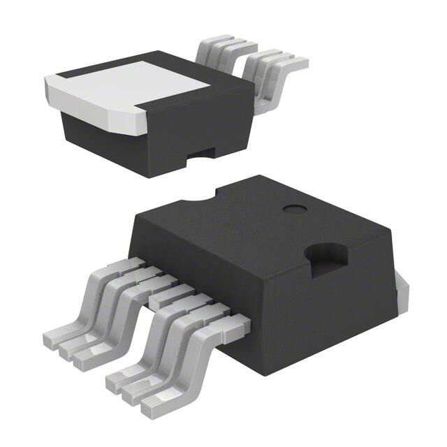
VN5T016AH-E
Datasheet
Single channel high-side driver with analog current sense
for 24 V automotive applications
Features
HP
AK
Description
HPAK
Parameter
Value
Max. transient supply voltage
VCC
58 V
Operating voltage range
VCC
8 to 36 V
Typ. on-state resistance (per channel)
RON
16 mΩ
Current limitation (typ.)
ILIM
60 A
Off-state supply current
IS
2 µA (1)
1. Typical value with all loads connected.
•
•
•
Product status link
VN5T016AH-E
Product summary
Order code
VN5T016AH-E
Package
HPAK
Packing
Tube
Order code
VN5T016AHTR-E
Package
HPAK
Packing
Tape and reel
•
AEC-Q100 qualified
General
–
Very low standby current
–
3.0 V CMOS compatible input
–
Optimized electromagnetic emission
–
Very low electromagnetic susceptibility
–
Compliant with European directive 2002/95/EC
–
Fault reset standby pin (FR_Stby)
–
Optimized for LED application
Diagnostic functions
–
Proportional load current sense
–
Current sense precision for wide range currents
–
Off-state open load detection
–
Output short to VCC detection
–
Overload and short to ground latch-off
–
Thermal shutdown latch-off
–
Very low current sense leakage
Protections
–
Undervoltage shutdown
–
Overvoltage clamp
–
Load current limitation
–
Self limiting of fast thermal transients
–
Protection against loss of ground and loss of VCC
–
–
–
Thermal shutdown
Reverse battery protected with self switch of the Power MOSFET
Electrostatic discharge protection
Applications
•
All types of resistive, inductive and capacitive loads
DS9252 - Rev 4 - May 2022
For further information contact your local STMicroelectronics sales office.
www.st.com
�VN5T016AH-E
Description
The VN5T016AH-E is a device made using STMicroelectronics VIPower technology,
intended for driving resistive or inductive loads with one side connected to ground.
Active VCC pin voltage clamp protects the device against low energy spikes.
The device integrates an analog current sense, which delivers a current proportional
to the load current.
Fault conditions such as overload, overtemperature, or short to VCC are reported via
the current sense pin.
Output current limitation protects the device in overload conditions. The device
latches off in case of overload or thermal shutdown.
The device is reset by a low level pass on the fault reset standby pin.
A permanent low level on the inputs and on the fault reset standby pin disables all
outputs and sets the device in standby mode.
DS9252 - Rev 4
page 2/31
�VN5T016AH-E
Block diagram and pin description
1
Block diagram and pin description
Figure 1. Block diagram
VCC
Signal Clamp
Reverse
battery
protection
Undervoltage
IN
Control & Diagnostic
Power
Clamp
DRIVER
CH1
VON
Limitation
Over
Temperature
Current
Limitation
OFF-state
Open-load
FR_Stby
VSENSEH
CS
Current
Sense
LOGIC
OUT
OVERLOAD PROTECTION
(ACTIVE POWER LIMITATION)
GND
GAPGCFT00198
Table 1. Pin function
Name
Function
VCC
Battery connection
OUT
Power output
GND
Ground connection
IN
Voltage controlled input pin with hysteresis, CMOS compatible. It controls output switch state
CS
Analog current sense pin, it delivers a current proportional to the load current
FR_Stby
In case of latch-off for overtemperature/overcurrent condition, a low pulse on the FR_Stby pin is
needed to reset the channel.
The device enters in standby mode if all inputs and the FR_Stby pin are low
DS9252 - Rev 4
page 3/31
�VN5T016AH-E
Block diagram and pin description
Figure 2. Configuration diagram (top view)
1
2
4
3
OUT GND IN
Vcc
5
6
7
GAPGCFT00653
CS FR_s tby OUT
Table 2. Suggested connections for unused and not connected pins
Connection/pin
CurrentSense
NC
Output
Input
FR_Stby
Floating
Not allowed
X(1)
X
X
X
To ground
Through 10 kΩ resistor
X
Not allowed
Through 10 kΩ resistor
Through 10 kΩ resistor
1. X: do not care.
DS9252 - Rev 4
page 4/31
�VN5T016AH-E
Electrical specification
2
Electrical specification
Figure 3. Current and voltage conventions
IS
VCC
IFR_Stby
OUT
FR_Stby
VFR_Stby
IIN
CS
IN
VIN
VF
IOUT
VCC
VOUT
ISENSE
VSENSE
GND
IGND
GAPGCFT00195
2.1
Absolute maximum ratings
Stressing the device above the ratings listed in the Table 3 may cause permanent damage to the device. These
are stress ratings only and operation of the device at these or any other conditions above those indicated in
the operating sections of this specification is not implied. Exposure to the conditions reported in this section for
extended periods may affect device reliability.
Table 3. Absolute maximum ratings
Symbol
Value
Unit
VCC
DC supply voltage
58
V
-VCC
Reverse DC supply voltage
-32
V
IOUT
DC output current
Internally limited
A
-IOUT
Reverse DC output current
30
A
DC input current
-1 to 10
mA
IFR_Stby
Fault reset standby DC input current
-1 to 1.5
mA
VCSENSE
Current sense maximum voltage
(VCC - 58) to VCC
V
IIN
EMAX
Maximum switching energy
(L = 10 mH; VBAT = 32 V; TJstart = 150 °C; IOUT = 5.9 A
390
mJ
Lsmax
Maximum stray inductance in short circuit condition
RL = 300 mΩ, VBAT = 32 V, TJstart = 150 °C, IOUT = IlimH (max.)
40
μH
VESD
VESD
TJ
DS9252 - Rev 4
Parameter
Electrostatic discharge (human body model: R = 1.5 kΩ, C = 100 pF)
Charge device model (CDM-AEC-Q100-011)
Junction operating temperature
IN
4000
CS
2000
FR_Stby
4000
OUT
5000
VCC
5000
V
750
V
-40 to 150
°C
page 5/31
�VN5T016AH-E
Thermal data
Symbol
Tstg
2.2
Parameter
Storage temperature
Value
Unit
-55 to 150
°C
Thermal data
Table 4. Thermal data
Symbol
2.3
Parameter
RthJC
Thermal resistance, junction-to-case
RthJA
Thermal resistance, junction-to-ambient
Value
Unit
1.5
°C/W
See Figure 27
°C/W
Electrical characteristics
8 V < VCC < 36 V, -40 °C < TJ < 150 °C, unless otherwise specified.
Table 5. Power section
Symbol
Parameter
Test conditions
Min.
Typ.
Max.
Unit
8
24
36
V
5
V
VCC
Operating supply voltage
VUSD
Undervoltage shutdown
3.5
Undervoltage shutdown hysteresis
0.5
VUSDhyst
IOUT = 5 A, TJ = 25 °C,
RON
On-state resistance
16
8 V < VCC < 36 V
mΩ
IOUT = 5 A, TJ = 150 °C,
32
8 V < VCC < 36 V
RON REV
Vclamp
Reverse battery on-state resistance
VCC = -24 V, IOUT = -5 A, TJ = 25 °C
Clamp voltage
IS = 20 mA
V
58
16
mΩ
64
70
V
2(1)
5
µA
2.5
5
mA
0.01
3
Off-state, VCC = 24 V, TJ = 25 °C,
VIN = VOUT = VSENSE = 0 V,
IS
Supply current
VFR_Stby = 0 V
On-state, VCC = 24 V,
VIN = 5 V, IOUT = 0 A
VIN = VOUT =0 V,
IL(off1)
Off-state output current
VCC = 24 V, TJ = 25 °C
VIN = VOUT =0 V,
VCC = 24 V, TJ = 125 °C
0
µA
0
5
1. Power MOSFET leakage included.
DS9252 - Rev 4
page 6/31
�VN5T016AH-E
Electrical characteristics
Table 6. Switching (VCC = 24 V, TJ = 25 °C)
Symbol
Parameter
Test conditions
Min.
Typ.
Max.
Unit
td(on)
Turn-on delay time
RL = 4.8 Ω
55
µs
td(off)
Turn-off delay time
RL = 4.8 Ω
53
µs
(dVOUT/dt)(on) Turn-on voltage slope
RL = 4.8 Ω
0.59
V/µs
(dVOUT/dt)(off) Turn-off voltage slope
RL = 4.8 Ω
0.54
V/µs
WON
Switching energy losses during twon
RL = 4.8 Ω
2.35
mJ
WOFF
Switching energy losses during twoff
RL = 4.8 Ω
1.05
mJ
Table 7. Logic inputs
Symbol
VIL
Input low level voltage
IIL
Low level input current
VIH
Input high level voltage
IIH
High level input current
VI(hyst)
Input hysteresis voltage
VICL
DS9252 - Rev 4
Parameter
Input clamp voltage
Test conditions
VIN = 0.9 V
IIN = 1 mA
Low level fault_reset_standby current
VFR_Stby_H
Fault_reset_standby high level
voltage
IFR_Stby_H
High level fault_reset_standby current VFR_Stby = 2.1 V
Fault_reset_standby clamp voltage
Unit
0.9
V
1
µA
2.1
V
10
7
-0.7
0.9
VFR_Stby = 0.9 V
V
V
1
µA
2.1
V
10
0.25
IFR_Stby = 15 mA (10 ms)
µA
V
5.5
IIN = -1 mA
IFR_Stby_L
VFR_Stby_CL
Max.
0.25
Fault_reset_standby low level voltage
Fault_reset_standby hysteresis
voltage
Typ.
VIN = 2.1 V
VFR_Stby_L
VFR_Stby(hyst)
Min.
V
11
IFR_Stby = -1 mA
µA
15
-0.7
V
V
treset
Overload latch-off reset time
See Figure 4
2
24
µs
tstby
Standby delay
See Figure 5
120
1200
µs
page 7/31
�VN5T016AH-E
Electrical characteristics
Figure 4. treset definition
treset
FR_Stby
IN
OUTPUT
CS
Overload
Channel
GAPGCFT000112
Figure 5. tstby definition
FR_Stby
INPUT
IGND
tstby
tstby
GAPGCFT000111
Table 8. Protections and diagnostics
Symbol
IlimH
DC short circuit current
IlimL
Short circuit current during thermal
cycling
TTSD
Shutdown temperature
TR
Reset temperature
TRS
Thermal reset of status
THYST
DS9252 - Rev 4
Parameter
Test conditions
VCC = 24 V
Turn-off output voltage clamp
VON
Output voltage drop limitation
Typ.
Max.
43
60
86
5 V < VCC < 36 V
Unit
A
86
VCC = 24 V, TR < TJ < TTSD
15
150
175
TRS + 1
TRS + 5
A
200
°C
°C
135
Thermal hysteresis (TTSD - TR)
VDEMAG
Min.
°C
7
°C
IOUT = 5 A, VIN = 0 V, L = 6 mH VCC - 58 VCC - 64 VCC - 70
IOUT = 500 mA,
TJ = -40 °C to 150 °C
25
V
mV
page 8/31
�VN5T016AH-E
Electrical characteristics
Table 9. Current sense (8 V < VCC < 36 V)
Symbol
dKLED/
KLEDTOT(1)
K0
dK0/K0(1)
K1
dK1/K1(1)
K2
Parameter
Test conditions
K3
dK3/K3(1)
K4
dK4/K4(1)
K5
dK5/K5(1)
K6
dK6/K6(1)
dK/Kbulb1(TOT)
(1)
DS9252 - Rev 4
Typ.
Max.
Unit
50
%
IOUT = 12 mA to 100 mA,
Current sense ratio drift
IOUTCAL = 50 mA, VSENSE = 0.5 V,
-50
TJ = -40 °C to 150 °C
IOUT/ISENSE
IOUT = 100 mA, VSENSE = 0.5 V,
TJ = -40 °C to 150 °C
1333
Current sense ratio drift
IOUT = 100 mA, VSENSE = 0.5 V,
TJ = -40 °C to 150 °C
-21
IOUT/ISENSE
Current sense ratio drift
IOUT/ISENSE
Current sense ratio drift
IOUT/ISENSE
Current sense ratio drift
IOUT/ISENSE
Current sense ratio drift
5600
11884
32
IOUT = 0.6 A, VSENSE = 1 V,
TJ = -40 °C to 150 °C
2418
IOUT = 0.6 A, VSENSE = 1 V,
TJ = 25 °C to 150 °C
3139
7981
IOUT = 0.6 A, VSENSE = 1 V,
TJ = -40 °C to 150 °C
-21
23
IOUT = 1.6 A, VSENSE = 1 V,
TJ = -40 °C to 150 °C
2928
7568
IOUT = 1.6 A, VSENSE = 1 V,
%
9264
5300
%
4700
3072
6693
IOUT = 1.6 A, VSENSE = 1 V,
TJ = -40 °C to 150 °C
-26
21
IOUT = 2.4 A, VSENSE = 2 V,
TJ = -40 °C to 150 °C
2912
IOUT = 2.4 A, VSENSE = 2 V,
TJ = 25 °C to 150 °C
3007
6039
IOUT = 2.4 A, VSENSE = 2 V,
TJ = -40 °C to 150 °C
-19
24
TJ = 25 °C to 150 °C
dK2/K2(1)
Min.
%
7048
4400
IOUT = 3 A, VSENSE = 4 V,
TJ = -40 °C to 150 °C
2843
IOUT = 3 A, VSENSE = 4 V,
TJ = 25 °C to 150 °C
3142
5634
IOUT = 3 A, VSENSE = 4 V,
TJ = -40 °C to 150 °C
-16
22
%
6686
4300
%
IOUT = 4.2 A, VSENSE = 4 V,
TJ = -40 °C to 150 °C
3034
IOUT = 4.2 A, VSENSE = 4 V,
TJ = 25 °C to 150 °C
3402
5276
Current sense ratio drift
IOUT = 4.2 A, VSENSE = 4 V,
TJ = -40 °C to 150 °C
-13
16
IOUT/ISENSE
IOUT = 20 A, VSENSE = 4 V,
TJ = -40 °C to 150 °C
3942
Current sense ratio drift
IOUT = 20 A, VSENSE = 4 V,
TJ = -40 °C to 150 °C
-5
5
%
Current sense ratio drift
IOUT = 1.6 A to 4.2 A, IOUTCAL = 3 A;
VSENSE = 4 V, TJ = -40 °C to 150 °C
-17
40
%
IOUT/ISENSE
5977
4250
4240
%
4748
page 9/31
�VN5T016AH-E
Electrical characteristics
Symbol
dK/Kbulb2(TOT)
(1)
Parameter
Current sense ratio drift
Test conditions
Min.
Max.
Unit
-31
33
%
IOUT = 0 A, VSENSE = 0 V, VIN = 0 V,
TJ = -40 °C to 150 °C
0
1
IOUT = 0 A, VSENSE = 0 V, VIN = 5 V,
TJ = -40 °C to 150 °C
0
5
IOUT = 0.6 A to 2.4 A, IOUTCAL = 1.2
A, VSENSE = 2 V,
Typ.
TJ = -40 °C to 150 °C
ISENSE0
Analog sense leakage current
µA
2
VSENSE
Max analog sense output voltage
IOUT = 20 A, RSENSE = 3.9 kΩ
VSENSEH
Analog sense output voltage in fault
condition(2)
VCC = 24 V, RSENSE = 3.9 kΩ
8
ISENSEH
Analog sense output current in fault
condition (2)
VCC = 24 V, VSENSE = 5 V
9
12
mA
300
600
µs
450
µs
3
20
µs
Min.
Typ.
Max.
Unit
2
-
4
V
180
-
1800
µs
-120
-
0
µA
-
20
µs
-
50
µs
V
V
VSENSE < 4 V, 0.5 A < IOUT < 20 A,
tDSENSE2H
Delay response time from rising edge
of INPUT pin
ISENSE = 90% of ISENSE max.,
(see Figure 6)
VSENSE < 4 V,
ΔtDSENSE2H
ISENSE = 90% of ISENSEMAX,
Delay response time between rising
edge of output current and rising edge IOUT = 90% of IOUTMAX,
of current sense
IOUTMAX = 5 A
(see Figure 10)
VSENSE < 4 V,
tDSENSE2L
Delay response time from falling edge 0.5 A < IOUT < 20 A,
of INPUT pin
I
= 10% of I
SENSE
SENSE
max
(see Figure 6)
1. Specified by design, not tested in production.
2. Fault condition includes: power limitation, overtemperature and openload in off-state condition.
Table 10. Openload detection (VFR_Stby = 5 V)
Symbol
Test conditions
VOL
Openload off-state voltage detection
threshold
VIN = 0 V, 8 V < VCC < 36 V
tDSTKON
Output short circuit to VCC detection
delay at turn off
See Figure 7
IL(off2)
Off-state output current at VOUT = 4 V
td_vol
Delay response from output rising
edge to VSENSE rising edge in
openload
tDFRSTK_ON
DS9252 - Rev 4
Parameter
Output short circuit to VCC detection
delay at FR_Stby activation
VIN = 0 V, VSENSE = 0 V,
VOUT rising from 0 V to 4 V
VOUT = 4 V, VIN = 0 V,
VSENSE = 90% of VSENSEH,
RSENSE = 3.9 kΩ
See Figure 9, Input = low
page 10/31
�VN5T016AH-E
Electrical characteristics
Figure 6. Current sense delay characteristics
INPUT
LOAD CURRENT
SENSE CURRENT
tDSENSE2L
tDSENSE2H
GAPGCFT000117
Figure 7. Openload off-state delay timing
Output stuck at VCC
VIN
VOUT > VOL
VSENSEH
VCS
tDSTKON
NOTE: VFR_stby = 5 V.
GAPGCFT000113
DS9252 - Rev 4
page 11/31
�VN5T016AH-E
Electrical characteristics
Figure 8. Switching characteristics
VOUT
tWon
tWoff
90%
80%
(dVOUT/dt)(off)
(dVOUT/dt)(on)
tr
tf
10%
t
INPUT
td(on)
td(off)
t
GAPGCFT000114
Figure 9. Output stuck to VCC detection delay time at FR_Stby activation
FR_Stby
VSENSEH
VCS
tDFRSTK_ON
Input = Low
GAPGCFT00038
DS9252 - Rev 4
page 12/31
�VN5T016AH-E
Electrical characteristics
Figure 10. Delay response time between rising edge of ouput current and rising edge of current sense
VIN
ΔtDSENSE2H
t
IOUT
IOUTMAX
90% IOUTMAX
t
ISENSE
ISENSEMAX
90% ISENSEMAX
t
GAPGCFT000115
Figure 11. Output voltage drop limitation
VCC - VOUT
TJ = 150 °C
TJ = 25 °C
TJ = -40 °C
VON
IOUT
VON /RON (T)
AG00074V1
DS9252 - Rev 4
page 13/31
�VN5T016AH-E
Electrical characteristics
Figure 12. Device behavior in overload condition
treset
treset
FAULT_RESET
IN
OUTPUT
VSENSEH
CS
overload
overload reset
overload diag reset
OVERLOAD(*)
CHANNEL
1
2
3
4
5 6
7
8
1: OUTPUT and CS controlled by IN
2: FAULT_RESET from ‘0’ to ‘1’ → no action on CS pin
3: overload latch-off. IN high → CS high
4: FAULT_RESET low AND Temp channel < overload_reset → overload latch reset after treset
4 to 5: FAULT_RESET low AND IN high → thermal cycling, CS high
5: FAULT_RESET high → latch-off reset disabled
6 to 7: overload event and FAULT_RESET high → latch-off, no thermal cycling
7 to 8: overload diagnostic disabled/enabled by the input
8: overload latch-off reset by FAULT_RESET
(*) OVERLOAD = thermal shutdown OR power limitation
GAPGCFT000116
Table 11. Truth table
Conditions
Standby
Normal operation
Overload
Overtemperature/short to ground
Undervoltage
Short to VBAT
Openload off-state (with pull-up)
Negative output voltage clamp
DS9252 - Rev 4
Fault reset
standby
Input
Output
Sense
L
L
X
0
X
L
L
0
X
H
H
Nominal
X
L
L
0
X
H
H
> Nominal
X
L
L
0
L
H
Cycling
VSENSEH
H
H
Latched
VSENSEH
X
X
L
0
L
L
H
0
H
L
H
VSENSEH
X
H
H
< Nominal
L
L
H
0
H
L
H
VSENSEH
X
H
H
0
X
L
Negative
0
page 14/31
�VN5T016AH-E
Electrical characteristics
Table 12. Electrical transient requirements (part 1)
ISO 7637-2:
Number of
Test levels(1)
2004(E)
III
IV
1
-450 V
-600 V
2a
37 V
+50 V
3a
-150 V
- 200 V
3b
+150 V
4
5b(2)
Test pulse
Burst cycle/pulse
pulses or
Delays and
impedence
repetition time
test times
5000
0.5 s
5s
1 ms, 50 Ω
0.2 s
5s
50 µs, 2 Ω
1h
90 ms
100 ms
0.1 µs, 50 Ω
+200 V
1h
90 ms
100 ms
0.1 µs, 50 Ω
-12 V
- 16 V
1 pulse
100 ms, 0.01 Ω
+123 V
+174 V
1 pulse
350 ms, 1 Ω
pulses
5000
pulses
1. The above test levels must be considered referred to VCC = 24.5 V except for pulse 5b.
2. Valid in case of external load dump clamp: 58 V maximum referred to ground.
Table 13. Electrical transient requirements (part 2)
ISO 7637-2:
Test level results
2004(E)
III
IV
1
C
C (1)
2a
C
C
3a
Test pulse
C
C
3b
(2)
E
E
3b
(3)
C
C
4
C
C
5b (4)
C
C
1. With Rload < 24 Ω.
2. Without capacitor between VCC and GND.
3. With 10 nF between VCC and GND.
4. External load dump clamp, 58 V maximum, referred to ground.
Table 14. Electrical transient requirements (part 3)
Class
DS9252 - Rev 4
Contents
C
All functions of the device are performed as designed after exposure to disturbance.
E
One or more functions of the device are not performed as designed after exposure to disturbance and cannot
be returned to proper operation without replacing the device.
page 15/31
�VN5T016AH-E
Electrical characteristics (curves)
2.4
Electrical characteristics (curves)
Figure 13. Off-state output current
Figure 14. High level input current
ILoff [u A]
IIH [uA]
6.00
5.0
4.5
5.00
VIN= 2.1V
4.0
3.5
4.00
Off-state
VCC= 24V
VIN=VOUT= 0
3.00
3.0
2.5
2.0
2.00
1.5
1.0
1.00
0.5
0.00
-50
-25
0
25
50
75
10 0
12 5
15 0
17 5
0.0
-50
-25
0
25
TC [°C]
50
75
10 0
TC [ °C]
GAPGCFT01029
Figure 15. Input clamp voltage
12 5
15 0
17 5
GAPGCFT01030
Figure 16. Input low level voltage
Vicl [V]
VIL [V]
7.0
2.0
6.8
1.8
IIN= 1mA
6.6
1.6
6.4
1.4
6.2
1.2
6.0
1.0
5.8
0.8
5.6
0.6
5.4
0.4
5.2
0.2
5.0
0.0
-50
-25
0
25
50
75
10 0
12 5
15 0
17 5
-50
-25
0
25
TC [ °C]
50
75
10 0
12 5
15 0
17 5
Tc [°C]
GAPGCFT01031
GAPGCFT01032
Figure 17. Input high level voltage
Figure 18. Input hysteresis voltage
VIH [V]
VI(hyst) [V]
4.0
1.0
3.5
0.9
0.8
3.0
0.7
2.5
0.6
2.0
0.5
1.5
0.4
0.3
1.0
0.2
0.5
0.1
0.0
0.0
-50
-25
0
25
50
75
TC [ °C]
DS9252 - Rev 4
10 0
12 5
15 0
17 5
-50
-25
0
25
50
75
10 0
12 5
15 0
17 5
TC [ °C]
GAPGCFT01033
GAPGCFT01034
page 16/31
�VN5T016AH-E
Electrical characteristics (curves)
Figure 20. On-state resistance vs VCC
Figure 19. On-state resistance vs TC
RON [mΩ]
RON [mΩ]
40
30
TC= 150 °C
25
30
TC= 125 °C
20
IOUT= 5A
VCC= 24V
15
20
TC= 25 °C
10
10
Tc= -40 °C
5
0
5.00
0
-50
-25
0
25
50
75
10 0
12 5
15 0
17 5
10 .00
15 .00
20 .00
TC [ °C]
25 .00
30 .00
35 .00
40 .00
VCC [V]
GAPGCFT01036
GAPGCFT01035
Figure 21. ILIMH vs TC
Figure 22. Turn-on voltage slope
(dVout/dt)on [V/us]
ILIMH [A]
2.0
65
1.8
64
VCC= 24V
1.6
63
VCC= 24V
RL= 4.8 Ω
1.4
1.2
62
1.0
61
0.8
60
0.6
0.4
59
0.2
58
-50
-25
0
25
50
75
10 0
12 5
15 0
0.0
17 5
-50
-25
0
TC [ °C]
25
50
75
10 0
12 5
15 0
17 5
TC [ °C]
GAPGCFT01037
GAPGCFT01038
Figure 23. Turn-off voltage slope
(dVout/dt)off [V/us]
1.40
1.20
VCC= 24V
RL= 4.8 Ω
1.00
0.80
0.60
0.40
0.20
0.00
-50
-25
0
25
50
75
TC [ °C]
DS9252 - Rev 4
10 0
12 5
15 0
17 5
GAPGCFT01039
page 17/31
�VN5T016AH-E
Application information
3
Application information
Figure 24. Application schematic
+5V
VCC
Rprot
FR_Stby
DId
MCU
Rprot
IN
Rprot
CS
OUT
GND
Cext
RSENSE
VGND
DGND
GAPGCFT000119
3.1
Load dump protection
Dld is necessary (voltage transient suppressor) if the load dump peak voltage exceeds the VCC maximum DC
rating. The same applies if the device is subject to transients on the VCC line that are greater than the ones shown
in the ISO 7637-2 2004 (E) in Table 12, Table 13 and Table 14.
3.2
MCU I/Os protection
If a ground protection network is used and negative transient is present on the VCC line, the control pins are
pulled negative. ST suggests that a resistor (Rprot) has to be inserted in line to prevent the microcontroller I/Os
pins from latching-up.
The value of these resistors is a compromise between the leakage current of the microcontroller and the current
required by the HSD I/Os (Input levels compatibility) with the latch-up limit of microcontroller I/Os.
Equation: Rprot range calculation
-VCCpeak/Ilatchup ≤ Rprot ≤ (VOHμC - VIH) / IIHmax
Calculation example:
For VCCpeak = -600 V and Ilatchup ≥ 20 mA; VOHμC ≥ 4.5 V
30 kΩ ≤ Rprot ≤ 190 kΩ.
Recommended Rprot value is 56 kΩ.
DS9252 - Rev 4
page 18/31
�VN5T016AH-E
Maximum demagnetization energy (VCC = 24 V)
4
Maximum demagnetization energy (VCC = 24 V)
Figure 25. Maximum turn off current versus inductance
100
Single pulse TJstart = 150 °C
Repetitive pulse TJstart = 100 °C
Repetitive pulse TJstart = 125 °C
B
C
A
I (A)
10
1
0.1
0.1
1
10
100
1000
L (mH)
GADG090520221346SA
Note:
DS9252 - Rev 4
Values are generated with RL = 0 Ω. In case of repetitive pulses, TJstart (at the beginning of each
demagnetization) of every pulse must not exceed the temperature specified above for curves A and B.
page 19/31
�VN5T016AH-E
Package and PCB thermal data
5
Package and PCB thermal data
5.1
HPAK thermal data
Figure 26. HPAK PCB
GAPGCFT00811
Layout condition of Rth and Zth measurements (board finish thickness 1.6 mm +/- 10%, board double layer, board
dimension 78x86, board material FR4, Cu thickness 0.070 mm (front and back side), thermal vias separation 1.2
mm, thermal via diameter 0.3 mm +/- 0.08 mm, Cu thickness on vias 0.025 mm, footprint dimension 6.4 mm x 7
mm).
Figure 27. RthJA vs PCB copper area in open box free air condition
RthJA (℃/W)
75
70
65
60
55
50
45
40
35
30
0
2
4
6
PCB Cu heat sink area (cm2)
DS9252 - Rev 4
8
10
GAPGCFT00812
page 20/31
�VN5T016AH-E
HPAK thermal data
Figure 28. HPAK thermal impedance junction ambient single pulse
10 0
Zth (°C/W)
A
B
C
10
1
t(s)
0.1
0.01
0.1
1
A: Cu = Footprint
10
10 0
B: Cu = 2 cm2
100 0
C: Cu = 8 cm2
GAPGCFT00813
Figure 29. Thermal fitting model of a single channel HSD in HPAK
TJ
C1
C2
C3
C4
C5
C6
R1
R2
R3
R4
R5
R6
Pd
GAPGCFT00280
The fitting model is a semplified thermal tool and is valid for transient evolutions where the embedded protections
(power limitation or thermal cycling during thermal shutdown) are not triggered.
Equation: pulse calculation formula
Zthδ = Rth · δ + Zthtp (1 - δ)
where δ = tP/T
DS9252 - Rev 4
page 21/31
�VN5T016AH-E
HPAK thermal data
Table 15. Thermal parameters
DS9252 - Rev 4
Area/island (cm2)
Footprint
R1 (°C/W)
0.1
R2 (°C/W)
0.5
R3 (°C/W)
2
R4 (°C/W)
8
R5 (°C/W)
4
8
28
22
14
R6 (°C/W)
31
25
18
C1 (W.s/°C)
0.01
C2 (W.s/°C)
0.05
C3 (W.s/°C)
0.2
C4 (W.s/°C)
0.4
C5 (W.s/°C)
0.8
1.4
3
C6 (W.s/°C)
3
6
9
page 22/31
�VN5T016AH-E
Package information
6
Package information
In order to meet environmental requirements, ST offers these devices in different grades of ECOPACK packages,
depending on their level of environmental compliance. ECOPACK specifications, grade definitions and product
status are available at: www.st.com. ECOPACK is an ST trademark.
DS9252 - Rev 4
page 23/31
�VN5T016AH-E
HPAK package information
6.1
HPAK package information
Figure 30. HPAK package dimensions
GAPGCFT00134_REV8
DS9252 - Rev 4
page 24/31
�VN5T016AH-E
HPAK packing information
Table 16. HPAK mechanical data
mm
Dim.
Min.
Max.
A
2.20
2.40
A1
0.90
1.10
A2
0.03
0.23
b
0.40
0.60
b1
0.45
0.65
b4
5.20
5.40
c
0.45
0.60
c2
0.48
0.60
D
6.00
6.20
D1
4.95
E
6.40
E1
5.00
e
5.10
5.25
6.60
5.20
5.40
0.85
e1
1.60
1.80
e2
3.30
3.50
e3
5.00
5.20
H
9.35
10.10
L
1
1.50
(L1)
2.60
2.80
3.00
L2
0.60
0.80
1.00
L4
0.50
R
1.00
0.20
V2
6.2
Typ.
0°
8°
HPAK packing information
Figure 31. HPAK tube shipment (no suffix)
GADG061120191325IG
DS9252 - Rev 4
page 25/31
�VN5T016AH-E
HPAK packing information
Figure 32. HPAK tape and reel (suffix “TR”)
GADG061120191328IG
DS9252 - Rev 4
page 26/31
�VN5T016AH-E
Revision history
Table 17. Document revision history
Date
Revision
Changes
01-Oct-2012
1
First release.
17-Sep-2013
2
Updated disclaimer.
Table 4: Thermal data:
24-Feb-2016
3
– Rthj-case: updated value
Updated Section 5.1: HPAK mechanical data
Modified Table 5. Power section
16-May-2022
4
Updated Figure 24. Application schematic
Updated Section 6.1 HPAK package information
Minor text changes.
DS9252 - Rev 4
page 27/31
�VN5T016AH-E
Contents
Contents
1
Block diagram and pin description . . . . . . . . . . . . . . . . . . . . . . . . . . . . . . . . . . . . . . . . . . . . . . . . . 3
2
Electrical specification. . . . . . . . . . . . . . . . . . . . . . . . . . . . . . . . . . . . . . . . . . . . . . . . . . . . . . . . . . . . . 5
3
2.1
Absolute maximum ratings. . . . . . . . . . . . . . . . . . . . . . . . . . . . . . . . . . . . . . . . . . . . . . . . . . . . . . . 5
2.2
Thermal data . . . . . . . . . . . . . . . . . . . . . . . . . . . . . . . . . . . . . . . . . . . . . . . . . . . . . . . . . . . . . . . . . . 6
2.3
Electrical characteristics. . . . . . . . . . . . . . . . . . . . . . . . . . . . . . . . . . . . . . . . . . . . . . . . . . . . . . . . . 6
2.4
Electrical characteristics (curves) . . . . . . . . . . . . . . . . . . . . . . . . . . . . . . . . . . . . . . . . . . . . . . . . 16
Application information . . . . . . . . . . . . . . . . . . . . . . . . . . . . . . . . . . . . . . . . . . . . . . . . . . . . . . . . . . .18
3.1
Load dump protection . . . . . . . . . . . . . . . . . . . . . . . . . . . . . . . . . . . . . . . . . . . . . . . . . . . . . . . . . . 18
3.2
MCU I/Os protection . . . . . . . . . . . . . . . . . . . . . . . . . . . . . . . . . . . . . . . . . . . . . . . . . . . . . . . . . . . 18
4
Maximum demagnetization energy (VCC = 24 V) . . . . . . . . . . . . . . . . . . . . . . . . . . . . . . . . . . .19
5
Package and PCB thermal data . . . . . . . . . . . . . . . . . . . . . . . . . . . . . . . . . . . . . . . . . . . . . . . . . . .20
5.1
6
HPAK thermal data . . . . . . . . . . . . . . . . . . . . . . . . . . . . . . . . . . . . . . . . . . . . . . . . . . . . . . . . . . . . 20
Package information. . . . . . . . . . . . . . . . . . . . . . . . . . . . . . . . . . . . . . . . . . . . . . . . . . . . . . . . . . . . . .23
6.1
HPAK package information . . . . . . . . . . . . . . . . . . . . . . . . . . . . . . . . . . . . . . . . . . . . . . . . . . . . . 24
6.2
HPAK packing information . . . . . . . . . . . . . . . . . . . . . . . . . . . . . . . . . . . . . . . . . . . . . . . . . . . . . . 25
Revision history . . . . . . . . . . . . . . . . . . . . . . . . . . . . . . . . . . . . . . . . . . . . . . . . . . . . . . . . . . . . . . . . . . . . . . .27
DS9252 - Rev 4
page 28/31
�VN5T016AH-E
List of figures
List of figures
Figure 1.
Figure 2.
Figure 3.
Figure 4.
Figure 5.
Figure 6.
Figure 7.
Figure 8.
Figure 9.
Figure 10.
Figure 11.
Figure 12.
Figure 13.
Figure 14.
Figure 15.
Figure 16.
Figure 17.
Figure 18.
Figure 19.
Figure 20.
Figure 21.
Figure 22.
Figure 23.
Figure 24.
Figure 25.
Figure 26.
Figure 27.
Figure 28.
Figure 29.
Figure 30.
Figure 31.
Figure 32.
DS9252 - Rev 4
Block diagram . . . . . . . . . . . . . . . . . . . . . . . . . . . . . . . . . . . . . . . . . . . . . . . . . . . . . .
Configuration diagram (top view). . . . . . . . . . . . . . . . . . . . . . . . . . . . . . . . . . . . . . . . . .
Current and voltage conventions. . . . . . . . . . . . . . . . . . . . . . . . . . . . . . . . . . . . . . . . . .
treset definition . . . . . . . . . . . . . . . . . . . . . . . . . . . . . . . . . . . . . . . . . . . . . . . . . . . . . .
tstby definition . . . . . . . . . . . . . . . . . . . . . . . . . . . . . . . . . . . . . . . . . . . . . . . . . . . . . . .
Current sense delay characteristics . . . . . . . . . . . . . . . . . . . . . . . . . . . . . . . . . . . . . . . .
Openload off-state delay timing. . . . . . . . . . . . . . . . . . . . . . . . . . . . . . . . . . . . . . . . . . .
Switching characteristics . . . . . . . . . . . . . . . . . . . . . . . . . . . . . . . . . . . . . . . . . . . . . . .
Output stuck to VCC detection delay time at FR_Stby activation . . . . . . . . . . . . . . . . . . . .
Delay response time between rising edge of ouput current and rising edge of current sense .
Output voltage drop limitation . . . . . . . . . . . . . . . . . . . . . . . . . . . . . . . . . . . . . . . . . . . .
Device behavior in overload condition . . . . . . . . . . . . . . . . . . . . . . . . . . . . . . . . . . . . . .
Off-state output current . . . . . . . . . . . . . . . . . . . . . . . . . . . . . . . . . . . . . . . . . . . . . . . .
High level input current . . . . . . . . . . . . . . . . . . . . . . . . . . . . . . . . . . . . . . . . . . . . . . . .
Input clamp voltage . . . . . . . . . . . . . . . . . . . . . . . . . . . . . . . . . . . . . . . . . . . . . . . . . . .
Input low level voltage . . . . . . . . . . . . . . . . . . . . . . . . . . . . . . . . . . . . . . . . . . . . . . . . .
Input high level voltage . . . . . . . . . . . . . . . . . . . . . . . . . . . . . . . . . . . . . . . . . . . . . . . .
Input hysteresis voltage . . . . . . . . . . . . . . . . . . . . . . . . . . . . . . . . . . . . . . . . . . . . . . . .
On-state resistance vs TC . . . . . . . . . . . . . . . . . . . . . . . . . . . . . . . . . . . . . . . . . . . . . .
On-state resistance vs VCC . . . . . . . . . . . . . . . . . . . . . . . . . . . . . . . . . . . . . . . . . . . . .
ILIMH vs TC . . . . . . . . . . . . . . . . . . . . . . . . . . . . . . . . . . . . . . . . . . . . . . . . . . . . . . . . .
Turn-on voltage slope . . . . . . . . . . . . . . . . . . . . . . . . . . . . . . . . . . . . . . . . . . . . . . . . .
Turn-off voltage slope . . . . . . . . . . . . . . . . . . . . . . . . . . . . . . . . . . . . . . . . . . . . . . . . .
Application schematic . . . . . . . . . . . . . . . . . . . . . . . . . . . . . . . . . . . . . . . . . . . . . . . . .
Maximum turn off current versus inductance. . . . . . . . . . . . . . . . . . . . . . . . . . . . . . . . . .
HPAK PCB. . . . . . . . . . . . . . . . . . . . . . . . . . . . . . . . . . . . . . . . . . . . . . . . . . . . . . . . .
RthJA vs PCB copper area in open box free air condition . . . . . . . . . . . . . . . . . . . . . . . . .
HPAK thermal impedance junction ambient single pulse. . . . . . . . . . . . . . . . . . . . . . . . . .
Thermal fitting model of a single channel HSD in HPAK . . . . . . . . . . . . . . . . . . . . . . . . . .
HPAK package dimensions . . . . . . . . . . . . . . . . . . . . . . . . . . . . . . . . . . . . . . . . . . . . .
HPAK tube shipment (no suffix) . . . . . . . . . . . . . . . . . . . . . . . . . . . . . . . . . . . . . . . . . .
HPAK tape and reel (suffix “TR”) . . . . . . . . . . . . . . . . . . . . . . . . . . . . . . . . . . . . . . . . . .
.
.
.
.
.
.
.
.
.
.
.
.
.
.
.
.
.
.
.
.
.
.
.
.
.
.
.
.
.
.
.
.
.
.
.
.
.
.
.
.
.
.
.
.
.
.
.
.
.
.
.
.
.
.
.
.
.
.
.
.
.
.
.
.
.
.
.
.
.
.
.
.
.
.
.
.
.
.
.
.
.
.
.
.
.
.
.
.
.
.
.
.
.
.
.
.
.
.
.
.
.
.
.
.
.
.
.
.
.
.
.
.
.
.
.
.
.
.
.
.
.
.
.
.
.
.
.
.
.
.
.
.
.
.
.
.
.
.
.
.
.
.
.
.
.
.
.
.
.
.
.
.
.
.
.
.
.
.
.
.
.
.
.
.
.
.
.
.
.
.
.
.
.
.
.
.
.
.
.
.
.
.
.
.
.
.
.
.
.
.
.
.
.
.
.
.
.
.
.
.
.
.
.
.
.
.
.
.
.
.
.
.
.
.
.
.
.
.
.
.
.
.
.
.
.
.
.
.
.
.
.
.
.
.
.
.
.
.
.
.
.
.
.
.
.
.
.
.
.
.
.
.
.
.
.
.
.
.
.
.
.
.
.
.
.
.
.
.
.
.
.
.
.
.
.
.
.
.
.
.
.
.
.
.
.
.
.
.
.
.
.
.
.
.
.
.
.
.
.
.
.
.
.
.
.
.
.
.
.
.
.
.
.
.
.
.
.
.
.
.
.
.
.
.
.
.
.
.
.
.
.
.
.
.
.
.
.
.
.
.
.
.
.
.
.
.
.
.
.
.
.
.
.
.
.
.
.
.
.
.
.
.
.
.
.
.
.
.
.
.
.
.
.
.
.
.
.
.
.
.
.
.
.
.
.
.
.
.
.
.
.
.
.
.
.
.
.
.
.
.
.
.
.
.
.
.
.
.
.
.
.
.
.
.
.
.
. 3
. 4
. 5
. 8
. 8
11
11
12
12
13
13
14
16
16
16
16
16
16
17
17
17
17
17
18
19
20
20
21
21
24
25
26
page 29/31
�VN5T016AH-E
List of tables
List of tables
Table 1.
Table 2.
Table 3.
Table 4.
Table 5.
Table 6.
Table 7.
Table 8.
Table 9.
Table 10.
Table 11.
Table 12.
Table 13.
Table 14.
Table 15.
Table 16.
Table 17.
Pin function . . . . . . . . . . . . . . . . . . . . . . . . . . . . . . . . . .
Suggested connections for unused and not connected pins .
Absolute maximum ratings . . . . . . . . . . . . . . . . . . . . . . .
Thermal data. . . . . . . . . . . . . . . . . . . . . . . . . . . . . . . . .
Power section . . . . . . . . . . . . . . . . . . . . . . . . . . . . . . . .
Switching (VCC = 24 V, TJ = 25 °C). . . . . . . . . . . . . . . . . .
Logic inputs. . . . . . . . . . . . . . . . . . . . . . . . . . . . . . . . . .
Protections and diagnostics. . . . . . . . . . . . . . . . . . . . . . .
Current sense (8 V < VCC < 36 V) . . . . . . . . . . . . . . . . . .
Openload detection (VFR_Stby = 5 V). . . . . . . . . . . . . . . . .
Truth table . . . . . . . . . . . . . . . . . . . . . . . . . . . . . . . . . .
Electrical transient requirements (part 1) . . . . . . . . . . . . . .
Electrical transient requirements (part 2) . . . . . . . . . . . . . .
Electrical transient requirements (part 3) . . . . . . . . . . . . . .
Thermal parameters . . . . . . . . . . . . . . . . . . . . . . . . . . . .
HPAK mechanical data . . . . . . . . . . . . . . . . . . . . . . . . . .
Document revision history . . . . . . . . . . . . . . . . . . . . . . . .
DS9252 - Rev 4
.
.
.
.
.
.
.
.
.
.
.
.
.
.
.
.
.
.
.
.
.
.
.
.
.
.
.
.
.
.
.
.
.
.
.
.
.
.
.
.
.
.
.
.
.
.
.
.
.
.
.
.
.
.
.
.
.
.
.
.
.
.
.
.
.
.
.
.
.
.
.
.
.
.
.
.
.
.
.
.
.
.
.
.
.
.
.
.
.
.
.
.
.
.
.
.
.
.
.
.
.
.
.
.
.
.
.
.
.
.
.
.
.
.
.
.
.
.
.
.
.
.
.
.
.
.
.
.
.
.
.
.
.
.
.
.
.
.
.
.
.
.
.
.
.
.
.
.
.
.
.
.
.
.
.
.
.
.
.
.
.
.
.
.
.
.
.
.
.
.
.
.
.
.
.
.
.
.
.
.
.
.
.
.
.
.
.
.
.
.
.
.
.
.
.
.
.
.
.
.
.
.
.
.
.
.
.
.
.
.
.
.
.
.
.
.
.
.
.
.
.
.
.
.
.
.
.
.
.
.
.
.
.
.
.
.
.
.
.
.
.
.
.
.
.
.
.
.
.
.
.
.
.
.
.
.
.
.
.
.
.
.
.
.
.
.
.
.
.
.
.
.
.
.
.
.
.
.
.
.
.
.
.
.
.
.
.
.
.
.
.
.
.
.
.
.
.
.
.
.
.
.
.
.
.
.
.
.
.
.
.
.
.
.
.
.
.
.
.
.
.
.
.
.
.
.
.
.
.
.
.
.
.
.
.
.
.
.
.
.
.
.
.
.
.
.
.
.
.
.
.
.
.
.
.
.
.
.
.
.
.
.
.
.
.
.
.
.
.
.
.
.
.
.
.
.
.
.
.
.
.
.
.
.
.
.
.
.
.
.
.
.
.
.
.
.
.
.
.
.
.
.
.
.
.
.
.
.
.
.
.
.
.
.
.
.
.
.
.
.
.
.
.
.
.
.
.
.
.
.
.
.
.
.
.
.
.
.
.
.
.
.
.
.
.
.
.
.
.
.
.
.
.
.
.
.
.
.
.
.
.
.
.
.
.
.
.
.
.
.
.
.
.
.
.
.
.
.
.
.
.
.
.
.
.
.
.
.
.
.
.
.
.
.
.
.
.
.
.
.
.
.
.
.
.
.
.
.
.
.
.
.
.
.
.
.
.
.
.
.
.
.
.
.
.
.
.
.
.
.
.
.
.
.
.
.
.
.
.
.
.
.
.
.
.
.
.
.
.
.
.
.
.
.
.
.
.
.
.
.
.
.
.
.
.
.
.
.
.
.
.
.
.
.
.
.
.
.
.
.
.
.
.
.
.
.
.
.
.
.
.
.
.
.
.
.
.
.
.
.
.
.
.
.
.
.
.
.
.
.
.
.
.
.
.
.
.
.
.
.
.
.
.
.
.
.
.
.
.
. 3
. 4
. 5
. 6
. 6
. 7
. 7
. 8
. 9
10
14
15
15
15
22
25
27
page 30/31
�VN5T016AH-E
IMPORTANT NOTICE – READ CAREFULLY
STMicroelectronics NV and its subsidiaries (“ST”) reserve the right to make changes, corrections, enhancements, modifications, and improvements to ST
products and/or to this document at any time without notice. Purchasers should obtain the latest relevant information on ST products before placing orders. ST
products are sold pursuant to ST’s terms and conditions of sale in place at the time of order acknowledgment.
Purchasers are solely responsible for the choice, selection, and use of ST products and ST assumes no liability for application assistance or the design of
purchasers’ products.
No license, express or implied, to any intellectual property right is granted by ST herein.
Resale of ST products with provisions different from the information set forth herein shall void any warranty granted by ST for such product.
ST and the ST logo are trademarks of ST. For additional information about ST trademarks, refer to www.st.com/trademarks. All other product or service names
are the property of their respective owners.
Information in this document supersedes and replaces information previously supplied in any prior versions of this document.
© 2022 STMicroelectronics – All rights reserved
DS9252 - Rev 4
page 31/31
�