VNH7070BAS
Automotive fully integrated H-bridge motor driver
Datasheet - production data
Description
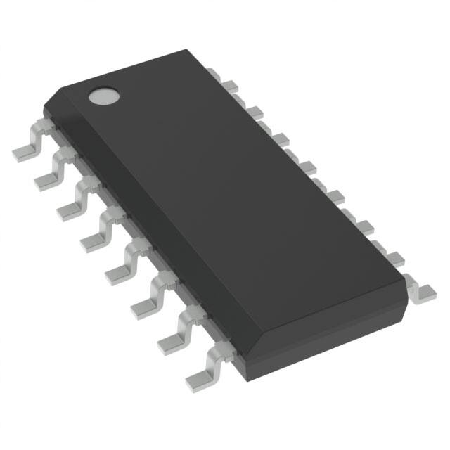
SO-16N
GAPGCFT00648
Features
Type
RDS(on)
Iout
VCCmax
VNH7070BAS
70 mtyp
per leg)
15 A
38 V
AEC-Q100 qualified
Output current: 15 A
3 V CMOS-compatible inputs
Undervoltage shutdown
Overvoltage clamp
Thermal shutdown
Cross-conduction protection
Current and power limitation
Very low standby power consumption
Protection against loss of ground and loss of
VCC
The device is a full bridge motor driver intended
for a wide range of automotive applications. The
device incorporates a dual monolithic high-side
driver and two low-side switches.
Both switches are designed using
STMicroelectronics’ well known and proven
proprietary VIPower® M0-7 technology that allows
to efficiently integrate on the same die a true
Power MOSFET with an intelligent
signal/protection circuitry. The three dies are
assembled in SO-16N package on electrically
isolated lead-frames.
Moreover, its fully symmetrical mechanical design
allows superior manufacturability at board level.
The input signals INA and INB can directly
interface the microcontroller to select the motor
direction and the brake condition. A SEL0 pin is
available to address the information available on
the CS to the microcontroller. The CS pin allows
to monitor the motor current by delivering a
current proportional to the motor current value.
The PWM, up to 20 kHz, allows to control the
speed of the motor in all possible conditions. In all
cases, a low level state on the PWM pin turns off
both the LSA and LSB switches.
Table 1. Device summary
PWM operation up to 20 kHz
CS diagnostic functions
– Analog motor current feedback
– Output short to ground detection
– Thermal shutdown indication
– OFF-state open-load detection
– Output short to VCC detection
Order codes
Package
SO-16N
Tube
Tape and reel
—
VNH7070BASTR
Output protected against short to ground and
short to VCC
Standby Mode
Half Bridge Operation
Package: ECOPACK®
March 2017
This is information on a product in full production.
DocID029595 Rev 2
1/38
www.st.com
�Contents
VNH7070BAS
Contents
1
Block diagram and pin description . . . . . . . . . . . . . . . . . . . . . . . . . . . . . 5
2
Electrical specifications . . . . . . . . . . . . . . . . . . . . . . . . . . . . . . . . . . . . . . 7
3
4
5
6
2/38
2.1
Absolute maximum ratings . . . . . . . . . . . . . . . . . . . . . . . . . . . . . . . . . . . . . 7
2.2
Thermal data . . . . . . . . . . . . . . . . . . . . . . . . . . . . . . . . . . . . . . . . . . . . . . . 8
2.3
Electrical characteristics . . . . . . . . . . . . . . . . . . . . . . . . . . . . . . . . . . . . . . . 9
2.4
Waveforms . . . . . . . . . . . . . . . . . . . . . . . . . . . . . . . . . . . . . . . . . . . . . . . . 20
Application information . . . . . . . . . . . . . . . . . . . . . . . . . . . . . . . . . . . . . 22
3.1
Reverse battery protection
. . . . . . . . . . . . . . . . . . . . . . . . . . . . . . . . . . . 23
3.2
OFF-state open-load detection – External circuitry dimensioning . . . . . . 23
3.3
Immunity against transient electrical disturbances . . . . . . . . . . . . . . . . . . 24
3.4
Device configurations . . . . . . . . . . . . . . . . . . . . . . . . . . . . . . . . . . . . . . . . 25
Package and PCB thermal data . . . . . . . . . . . . . . . . . . . . . . . . . . . . . . . 27
4.1
SO16-N thermal data . . . . . . . . . . . . . . . . . . . . . . . . . . . . . . . . . . . . . . . . 27
4.2
Package thermal data . . . . . . . . . . . . . . . . . . . . . . . . . . . . . . . . . . . . . . . 28
4.2.1
Thermal characterization in steady state conditions . . . . . . . . . . . . . . . 28
4.2.2
Thermal characterization during transients . . . . . . . . . . . . . . . . . . . . . . 29
Package and packing information . . . . . . . . . . . . . . . . . . . . . . . . . . . . . 33
5.1
SO-16N mechanical data . . . . . . . . . . . . . . . . . . . . . . . . . . . . . . . . . . . . . 33
5.2
SO-16N packing information . . . . . . . . . . . . . . . . . . . . . . . . . . . . . . . . . . 34
5.3
SO-16N marking information . . . . . . . . . . . . . . . . . . . . . . . . . . . . . . . . . . 36
Revision history . . . . . . . . . . . . . . . . . . . . . . . . . . . . . . . . . . . . . . . . . . . 37
DocID029595 Rev 2
�VNH7070BAS
List of tables
List of tables
Table 1.
Table 2.
Table 3.
Table 4.
Table 5.
Table 6.
Table 7.
Table 8.
Table 9.
Table 10.
Table 11.
Table 12.
Table 13.
Table 14.
Table 15.
Table 16.
Table 17.
Table 18.
Table 19.
Table 20.
Device summary . . . . . . . . . . . . . . . . . . . . . . . . . . . . . . . . . . . . . . . . . . . . . . . . . . . . . . . . . . 1
Block description. . . . . . . . . . . . . . . . . . . . . . . . . . . . . . . . . . . . . . . . . . . . . . . . . . . . . . . . . . 5
Pin definitions and functions . . . . . . . . . . . . . . . . . . . . . . . . . . . . . . . . . . . . . . . . . . . . . . . . . 6
Absolute maximum ratings . . . . . . . . . . . . . . . . . . . . . . . . . . . . . . . . . . . . . . . . . . . . . . . . . . 7
Thermal data. . . . . . . . . . . . . . . . . . . . . . . . . . . . . . . . . . . . . . . . . . . . . . . . . . . . . . . . . . . . . 8
Power section . . . . . . . . . . . . . . . . . . . . . . . . . . . . . . . . . . . . . . . . . . . . . . . . . . . . . . . . . . . . 9
Logic inputs (INA, INB) (VCC = 7 V up to 28 V; -40 °C < Tj < 150 °C) . . . . . . . . . . . . . . . . . 10
Switching (VCC = 13 V, RLOAD = 3.7 Ω) . . . . . . . . . . . . . . . . . . . . . . . . . . . . . . . . . . . . . . . 10
Protections and diagnostics (VCC = 7 V up to 18 V; -40 °C < Tj < 150 °C). . . . . . . . . . . . . 11
CS (7 V < VCC < 18 V) . . . . . . . . . . . . . . . . . . . . . . . . . . . . . . . . . . . . . . . . . . . . . . . . . . . . 12
Operative condition - truth table . . . . . . . . . . . . . . . . . . . . . . . . . . . . . . . . . . . . . . . . . . . . . 18
On-state fault conditions- truth table . . . . . . . . . . . . . . . . . . . . . . . . . . . . . . . . . . . . . . . . . . 18
Off-state -truth table . . . . . . . . . . . . . . . . . . . . . . . . . . . . . . . . . . . . . . . . . . . . . . . . . . . . . . 19
ISO 7637-2 - electrical transient conduction along supply line . . . . . . . . . . . . . . . . . . . . . . 24
Thermal model for junction temperature calculation in steady-state conditions . . . . . . . . . 29
Thermal parameters . . . . . . . . . . . . . . . . . . . . . . . . . . . . . . . . . . . . . . . . . . . . . . . . . . . . . . 31
SO-16N mechanical data . . . . . . . . . . . . . . . . . . . . . . . . . . . . . . . . . . . . . . . . . . . . . . . . . . 34
Reel dimensions . . . . . . . . . . . . . . . . . . . . . . . . . . . . . . . . . . . . . . . . . . . . . . . . . . . . . . . . . 35
SO-16N carrier tape dimensions. . . . . . . . . . . . . . . . . . . . . . . . . . . . . . . . . . . . . . . . . . . . . 35
Document revision history. . . . . . . . . . . . . . . . . . . . . . . . . . . . . . . . . . . . . . . . . . . . . . . . . . 37
DocID029595 Rev 2
3/38
3
�List of figures
VNH7070BAS
List of figures
Figure 1.
Figure 2.
Figure 3.
Figure 4.
Figure 5.
Figure 6.
Figure 7.
Figure 8.
Figure 9.
Figure 10.
Figure 11.
Figure 12.
Figure 13.
Figure 14.
Figure 15.
Figure 16.
Figure 17.
Figure 18.
Figure 19.
Figure 20.
Figure 21.
Figure 22.
Figure 23.
Figure 24.
Figure 25.
Figure 26.
Figure 27.
Figure 28.
Figure 29.
Figure 30.
Figure 31.
Figure 32.
4/38
Block diagram . . . . . . . . . . . . . . . . . . . . . . . . . . . . . . . . . . . . . . . . . . . . . . . . . . . . . . . . . . . . 5
Configuration diagram (top view) . . . . . . . . . . . . . . . . . . . . . . . . . . . . . . . . . . . . . . . . . . . . . 6
Current and voltage conventions . . . . . . . . . . . . . . . . . . . . . . . . . . . . . . . . . . . . . . . . . . . . . 7
TDSTKON . . . . . . . . . . . . . . . . . . . . . . . . . . . . . . . . . . . . . . . . . . . . . . . . . . . . . . . . . . . . . . . . . . . . . . . . . . . . . . . . 13
Definition of the low-side switching times . . . . . . . . . . . . . . . . . . . . . . . . . . . . . . . . . . . . . . 14
Definition of the high-side switching times . . . . . . . . . . . . . . . . . . . . . . . . . . . . . . . . . . . . . 14
Low-side turn-on delay time . . . . . . . . . . . . . . . . . . . . . . . . . . . . . . . . . . . . . . . . . . . . . . . . 15
Time to shutdown for the low-side driver . . . . . . . . . . . . . . . . . . . . . . . . . . . . . . . . . . . . . . 15
Input reset time for HSD - fault unlatch. . . . . . . . . . . . . . . . . . . . . . . . . . . . . . . . . . . . . . . . 16
Input reset time for LSD - fault unlatch . . . . . . . . . . . . . . . . . . . . . . . . . . . . . . . . . . . . . . . . 16
OFF-state diagnostic delay time from rising edge of VOUT (tD_VOL) . . . . . . . . . . . . . . . . . . 17
Normal operative conditions . . . . . . . . . . . . . . . . . . . . . . . . . . . . . . . . . . . . . . . . . . . . . . . . 20
OUT shorted to ground and short clearing . . . . . . . . . . . . . . . . . . . . . . . . . . . . . . . . . . . . . 20
OUT shorted to Vcc and short clearing. . . . . . . . . . . . . . . . . . . . . . . . . . . . . . . . . . . . . . . . 21
Application schematic with reverse battery protection connected to Vbatt . . . . . . . . . . . . . 22
Application schematic with reverse battery protection connected to GND . . . . . . . . . . . . . 22
Suggested PCB layout . . . . . . . . . . . . . . . . . . . . . . . . . . . . . . . . . . . . . . . . . . . . . . . . . . . . 23
Half-bridge configuration (case a). . . . . . . . . . . . . . . . . . . . . . . . . . . . . . . . . . . . . . . . . . . . 25
Half-bridge configuration (case b). . . . . . . . . . . . . . . . . . . . . . . . . . . . . . . . . . . . . . . . . . . . 25
Multi-motors configuration. . . . . . . . . . . . . . . . . . . . . . . . . . . . . . . . . . . . . . . . . . . . . . . . . . 26
PCB layout (top and bottom): footprint, 2+2+2 cm2, 8+8+8 cm2 . . . . . . . . . . . . . . . . . . . . . . . . . . 27
PCB 4 layer. . . . . . . . . . . . . . . . . . . . . . . . . . . . . . . . . . . . . . . . . . . . . . . . . . . . . . . . . . . . . 28
Chipset configuration in steady state conditions. . . . . . . . . . . . . . . . . . . . . . . . . . . . . . . . . 28
Auto and mutual Rthj-amb vs. PCB heat-sink area in open box free air condition . . . . . . . . 29
HSD thermal impedance junction ambient single pulse . . . . . . . . . . . . . . . . . . . . . . . . . . . 30
LSD thermal impedance junction ambient single pulse . . . . . . . . . . . . . . . . . . . . . . . . . . . 30
Electrical equivalent model . . . . . . . . . . . . . . . . . . . . . . . . . . . . . . . . . . . . . . . . . . . . . . . . . 31
SO-16N package dimensions . . . . . . . . . . . . . . . . . . . . . . . . . . . . . . . . . . . . . . . . . . . . . . . 33
SO-16N reel 13” . . . . . . . . . . . . . . . . . . . . . . . . . . . . . . . . . . . . . . . . . . . . . . . . . . . . . . . . . 34
SO-16N rcarrier tape. . . . . . . . . . . . . . . . . . . . . . . . . . . . . . . . . . . . . . . . . . . . . . . . . . . . . . 35
SO-16N schematic drawing of leader and trailer tape . . . . . . . . . . . . . . . . . . . . . . . . . . . . 36
SO-16N marking information . . . . . . . . . . . . . . . . . . . . . . . . . . . . . . . . . . . . . . . . . . . . . . . 36
DocID029595 Rev 2
�VNH7070BAS
1
Block diagram and pin description
Block diagram and pin description
Figure 1. Block diagram
V CC
POWER
LIMITATION
LSA_OVERTEMPERATURE
LSB_OVERTEMPERATURE
UV
HSA_OVERTEMPERATURE
HSB_OVERTEMPERATURE
CLAMP HS A
HS A
CLAMP HS B
DRIVER
HS A
Open-load
OFF-state A
HS B
DRIVER
HS B
LOGIC
Open-load
OFF-state B
CURRENT
LIMITATION B
CURRENT
LIMITATION A
FAULT
OUT A
1/K
DETECTION
OUT B
1/K
CLAMP LS A
CLAMP LS B
DRIVER
LS A
LS A
DRIVER
LS B
MUX
LS B
OVERLOAD
DETECTOR B
OVERLOAD
DETECTOR A
IN A
GND A
CS
SEL0 INB PWM
GND B
GAPGCFT01189
Table 2. Block description
Name
Description
Logic control
Allows the turn-on and the turn-off of the high-side and the
low-side switches according to the truth table.
Undervoltage
Shuts down the device for battery voltage lower than 4 V.
High-side and low-side clamp voltage
Protect the high-side and the low-side switches from the
high voltage on the battery line.
High-side and low-side driver
Drive the gate of the concerned switch to allow a proper
Ron for the leg of the bridge.
Current limitation
Limits the motor current in case of short circuit.
In case of short-circuit with the increase of the junction
High-side and low-side overtemperature
temperature, it shuts down the concerned driver to prevent
protection
degradation and to protect the die.
Low-side overload detector
Detects when low side current exceeds shutdown current
and latches off the concerned Low side.
DocID029595 Rev 2
5/38
37
�Block diagram and pin description
VNH7070BAS
Table 2. Block description (continued)
Name
Description
Fault detection
Signalizes the abnormal behavior of the switch through CS
pin.
Power limitation
Limits the power dissipation of the high-side driver inside
safe range in case of short to ground condition.
Figure 2. Configuration diagram (top view)
*1'$
�
��
*1'$
287$
�
��
287$
,1 $
9&&
�
��
6(/ �
�
��
9&&
�
&6
9&&
,1%
�
��
3:0
287%
�
��
287%
*1'%
�
�
*1'%
62���1
��
*$3*&)7�����
Table 3. Pin definitions and functions
6/38
Pin N°
Symbol
Function
1, 16
GNDA
Source of low-side switch A
2, 15
OUTA
Source of high-side switch A / drain of low-side switch A
3
INA
Clockwise input
4, 5, 12
VCC
Power supply voltage
6
INB
Counter clockwise input
7, 10
OUTB
Source of high-side switch B / drain of low-side switch B
8, 9
GNDB
Source of low-side switch B
11
PWM
Voltage controlled input pin with hysteresis, CMOS compatible. Gates
of low-side FETS get modulated by the PWM signal during their on
phase allowing speed control of the motor
13
CS
Multiplexed analog sense output pin; it delivers a current proportional
to the motor current according to the leg selection.
14
SEL0
Active high compatible with 3 V and 5 V CMOS outputs pin; in
combination with INA, INB, it addresses the CurrentSense information
delivered to the micro according to the operative truth table.
DocID029595 Rev 2
�VNH7070BAS
2
Electrical specifications
Electrical specifications
Figure 3. Current and voltage conventions
*4
**/"
**/#
*065"
7$$
*/"
065"
*/#
*4&-�
*18.
*065#
065#
4&-�
(/%
7065"
*4&/4&
����������������$4
18.
7$$
74&/4&
7065#
*(/%
7*/" 7*/# 74&-� 718.
("1($'5�����
2.1
Absolute maximum ratings
Stressing the device above the rating listed in Table 4: Absolute maximum ratings may
cause permanent damage to the device. These are stress ratings only and operation of the
device at these or any other conditions above those indicated in the Operating sections of
this specification is not implied. Exposure to Absolute Maximum Rating conditions for
extended periods may affect device reliability.
Table 4. Absolute maximum ratings
Symbol
Parameter
Value
Unit
VCC
Supply voltage
38
V
-VCC
Reverse DC Supply Voltage
0.3
V
Imax
Maximum output current (continuous)
Internally limited
A
Reverse output current (continuous)
-15
A
VCCPK
Maximum transient supply voltage (ISO 16750-2:2010
Test B clamped to 40 V; RL = 4 )
40
V
VCCJS
Maximum jump start voltage for single pulse short circuit
protection
28
V
Input current (INA and INB pins)
-1 to 10
mA
ISEL0
SEL0 DC input current
-1 to 10
mA
IPWM
PWM input current
-1 to 10
mA
IR
IIN
ISENSE
CS pin DC output current (VGND = VCC and VSENSE < 0 V
10
CS pin DC output current in reverse (VCC < 0 V)
-20
DocID029595 Rev 2
mA
7/38
37
�Electrical specifications
VNH7070BAS
Table 4. Absolute maximum ratings (continued)
Symbol
Value
Unit
VESD
Electrostatic discharge
(Human body model: R = 1.5 k; C = 100 pF)
– INA, INB, PWM
– SEL0
– CS
– VCC
– Output
2
2
2
4
4
VESD
Charge device model (CDM-AEC-Q100-011)
750
V
Junction operating temperature
-40 to 150
°C
Storage temperature
-55 to 150
°C
Tc
TSTG
2.2
Parameter
kV
Thermal data
Table 5. Thermal data
Symbol
Rthj-pin
Parameter
Thermal resistance junction-pin
Rthj-amb Thermal resistance junction-ambient (JEDEC JESD
2. Device mounted on four-layers 2s2p PCB.
8/38
DocID029595 Rev 2
Unit
HSD
31
°C/W
LSD
44
°C/W
51-2)(1)
Rthj-amb Thermal resistance junction-ambient (JEDEC JESD 51-2)(2)
1. Device mounted on two-layers 2s0p PCB.
Max. value
See Figure 24 °C/W
HSD
39.5
°C/W
LSD
55
°C/W
�VNH7070BAS
2.3
Electrical specifications
Electrical characteristics
Values specified in this section are for VCC = 7 V up to 28 V; -40 °C < Tj < 150 °C, unless
otherwise specified.
Table 6. Power section
Symbol
VCC
IS
tD_sdby(1)
Parameter
Test conditions
Operating supply
voltage
Supply current
V
Off-state - standby; INA = INB = 0;
SEL0 = 0; PWM = 0; Tj = 25 °C;
VCC = 13 V
1
μA
Off-state - standby; INA = INB = 0;
SEL0 = 0; PWM = 0; VCC = 13 V;
Tj = 85 °C
1
μA
Off-state - standby; INA = INB = 0;
SEL0 = 0; PWM = 0; VCC = 13 V;
Tj = 125 °C
3
μA
Off-state (no standby);
INA = INB = 0; SEL0 = 5 V;
PWM = 0
2
4
mA
On-state: INA or INB = 5 V;
PWM = 0 V or PWM=5 V;
SEL0 = X
3.5
6
mA
1
1.8
ms
VCC =13 V;
Standby mode blanking
INA = INB= PMW = 0 V;
time
VSEL0 from 5 V to 0 V
IOUT = 3.5 A; Tj = 25°C
RONLS
Static low-side
resistance
IOUT = 3.5 A; Tj = 25°C
IL(off_h)
0.2
42
IOUT = 3.5 A; Tj = -40 to 150°C
30
Off-state output current
INA = 0; INB = 5 V; PWM = 0;
of one leg with other
VCC = 13 V
HSD on
m
m
60
m
0.9
V
0
0.5
μA
0
3
μA
20
60
μA
IOUT = -3.5 A; Tj = 150°C
INA = INB = 0; PWM = 0;
Off-state output current VCC = 13 V; Tj = 25 °C
of one leg
INA = INB = 0; PWM = 0;
VCC = 13 V; Tj = 125 °C
m
85
IOUT = 3.5 A; Tj = -40°C to 150°C
Free-wheeling diode
forward voltage
Max. Unit
28
Static high-side
resistance
IL(off)
Typ.
4
RONHS
Vf
Min.
0.7
1. To power on the device from the standby, it is recommended to:
— toggle INA or INB or SEL0 from 0 to 1 first to come out from STBY mode
— toggle PWM from 0 to 1 with a delay of 20 μs
this avoids any over-stress on the device in case of existing short-to-battery.
DocID029595 Rev 2
9/38
37
�Electrical specifications
VNH7070BAS
Table 7. Logic inputs (INA, INB) (VCC = 7 V up to 28 V; -40 °C < Tj < 150 °C)
Symbol
Parameter
Test conditions
Min.
Typ.
Max.
Unit
0.9
V
VIL
Input low level voltage
VIH
Input high level voltage
2.1
V
VIHYST
Input hysteresis voltage
0.2
V
IIN = 1 mA
VICL
Input clamp voltage
IINL
Input current
VIN = 0.9 V
IINH
Input current
VIN = 2.1 V
5.3
IIN = -1 mA
7.2
-0.7
V
V
1
μA
10
μA
0.9
V
SEL0 (VCC = 7 V up to 18 V; -40°C < Tj < 150°C)
VSELL
Input low level voltage
ISELL
Low level input current
VSELH
Input high level voltage
ISELH
High level input current
VSEL(hyst)
Input hysteresis voltage
VSELCL
Input clamp voltage
VSEL = 0.9 V
1
μA
2.1
V
VSEL = 2.1 V
10
0.2
ISEL = 1 mA
V
5.3
ISEL = -1 mA
μA
7.5
-0.7
V
V
PWM (VCC= 7 V up to 28 V; -40°C < Tj < 150°C)
VPWM
Input low level voltage
IPWM
Low level input current
VPWM
Input high level voltage
IPWMH
High level input current
0.9
VPMW = 0.9 V
VPMWCL
Input clamp voltage
1
μA
2.1
V
VPMW = 2.1 V
VPWM(hyst) Input hysteresis voltage
10
0.2
IPMW = 1 mA
V
V
5.3
IPMW = -1 mA
μA
7.2
-0.7
V
V
Table 8. Switching (VCC = 13 V, RLOAD = 3.7 Ω)
Symbol
f(1)
Parameter
Test conditions
PWM frequency
Min.
Typ.
0
Unit
20
kHz
td(on)
Turn-on delay time
Input rise time < 1μs
(see Figure 6)
25
μs
td(off)
Turn-off delay time
Input rise time < 1μs
(see Figure 6)
15
μs
tr
Rise time
See Figure 5
0.7
1.5
μs
tf
Fall time
See Figure 5
0.2
0.5
μs
Low-side turn-on delay
time
Input rise time < 1 μs (see
Figure 7)
140
350
μs
tcross
40
1. Parameter guaranteed by design and characterization; not subjected to production test.
10/38
Max.
DocID029595 Rev 2
�VNH7070BAS
Electrical specifications
Table 9. Protections and diagnostics (VCC = 7 V up to 18 V; -40 °C < Tj < 150 °C)
Symbol
Parameter
Test conditions
Min. Typ. Max. Unit
VUSD
Undervoltage shutdown
4
V
VUSDreset
Undervoltage shutdown
reset
5
V
VUSDHyst
Undervolatge shutdown
Hysteresis
0.4
V
ILIM_H
High-side current
limitation
15
22
30
A
ISD_LS
Shutdown LS current
18
27
36
A
tSD_LS
Time to shutdown for the INA = 5 V; INB = 0 V;
low-side
PWM = 5 V (see Figure 8)
5
μs
VCL_HSD
High-side clamp voltage
(VCC to OUTA = 0 or
OUTB = 0)
IOUT = 100 mA; tclamp = 1 ms
38
46
V
VCL_LSD
Low-side clamp voltage
(OUTA = VCC or
OUTB = VCC to GND)
IOUT = 100 mA; tclamp = 1 ms
38
46
V
TTSD_HS
High-side thermal
shutdown temperature
INx = 2.1 V
150
175
TTR_HS
High-side thermal reset
temperature
THYST_HS
High-side thermal
hysteresis (TSD_HS - T
R_HS)
TTSD_LS
Low-side thermal
shutdown temperature
INx = 0 V
150
175
200
°C
VCL
Total clamp voltage
(VCC to GND)
IOUT = 100 mA; tclamp = 1 ms
38
46
52
V
VOL
OFF-state open-load
voltage detection
threshold
INA = INB = 0 V; PWM = 0;
VSEL0 = 5 V for CHA;
VSEL0 = 0 V and within
td_stby for CHB
2
3
4
V
IL(off2)
OFF-state output sink
current
INA = INB = 0; VOUT = VOL;
PWM = 0 V;
VSEL0 = 5 V for CHA;
VSEL0 = 0 V and within
td_stby for CHB
-100
-15
μA
tDSTKON
OFF-state diagnostic
delay time from falling
edge of INPUT (see
Figure 4)
INA = 5 V to 0 V; INB = 0;
VSEL0 = 5 V; PWM = 0;
IOUT = 0 A; VOUTA = 4 V
350
μs
200
135
°C
7
DocID029595 Rev 2
40
°C
140
°C
11/38
37
�Electrical specifications
VNH7070BAS
Table 9. Protections and diagnostics (VCC = 7 V up to 18 V; -40 °C < Tj < 150 °C)
Symbol
tD_VOL
Parameter
Test conditions
OFF-state diagnostic
delay time from rising
edge of VOUT (see
Figure 11)
Min. Typ. Max. Unit
INA = INB = 0 V; PWM = 0;
VOUTx = 0 V to 4 V;
VSEL0 = 5 V for CHA;
VSEL0 = 0 V and within
td_stby for CHB
5
30
μs
Input reset time for high
tLATCH_RST_HS(1) side fault unlatch (see
Figure 9)
VINx = 5 V to 0 V; HSDx
faulting
3
10
20
μs
Input reset time for low
tLATCH_RST_LS(1) side fault unlatch (see
Figure 10)
VINx = 0 V to 5 V; LSDx
faulting
3
10
20
μs
1. Parameter guaranteed by design and characterization; not subjected to production test.
Table 10. CS (7 V < VCC < 18 V)
Symbol
VSENSE_CL
12/38
Parameter
Test conditions
Min.
VCC = 18 V; ISENSE = -5 mA
Multisense clamp
voltage
Typ.
Max.
Unit
-9
V
11
VCC = 18 V; ISENSE = 5 mA
-13
K0
IOUT/ISENSE
IOUT = 0.05 A; VSENSE = 0.5 V;
Tj = -40°C to 150°C
665
K1
IOUT/ISENSE
IOUT = 0.2 A; VSENSE = 0.5 V;
Tj = -40°C to 150°C
1083
1900
2716
K2
IOUT/ISENSE
IOUT = 3.5 A; VSENSE = 4 V;
Tj = -40°C to 150°C
1315
1540
1779
K3
IOUT/ISENSE
IOUT = 5.5 A; VSENSE = 4 V;
Tj = -40°C to 150°C
1357
1540
1727
dK0/K0(1)(2)
Analog sense
current drift
IOUT = 0.05 A; VSENSE = 0.5 V;
Tj = -40°C to 150°C
-25
25
%
dK1/K1(1)(2)
Analog sense
current drift
IOUT = 0.2 A; VSENSE = 0.5 V;
Tj = -40°C to 150°C
-21
21
%
dK2/K2(1)(2)
Analog sense
current drift
IOUT = 3.5 A; VSENSE = 4 V;
Tj = -40°C to 150°C
-5
5
%
dK3/K3(1)(2)
Analog sense
current drift
IOUT = 5.5 A; VSENSE = 4 V;
Tj = -40°C to 150°C
-4
4
%
VSENSESAT
Max analog sense
output voltage
VCC = 7; RSENSE = 10 kΩ;
VSEL0 = 5 V; IOUTA = 5.5 A;
VINA = 5 V; PWM = 0;
Tj = 150°C
5
V
ISENSE_SAT(2)
CurrentSense
saturation current
VCC = 13 V; VINA = 5 V;
VINB = 0 V; VSENSE = 4 V;
VSEL0 = 5 V; Tj = 150°C
4.6
mA
IOUT_SAT(2)
Output saturation
current
VCC = 13 V; VSENSE = 4 V;
VINA = 5 V; VINB = 0 V;
VSEL0 = 5 V; Tj = 150°C
8
A
DocID029595 Rev 2
�VNH7070BAS
Electrical specifications
Table 10. CS (7 V < VCC < 18 V) (continued)
Symbol
Parameter
Test conditions
Output Voltage for
VOUT_MSD(2) MultiSense
shutdown
Min.
Typ.
VINA = 5 V; VINB = 0 V;
VSEL0 = 5 V; RSENSE = 2.7 kΩ;
IOUT = 3.5 A
Max.
Unit
5
V
IOUT = 0 A; VSENSE = 0 V;
INx = 0 V; SEL0 = 0;
Tj = -40°C to 150°C (Standby)
0
0.5
μA
IOUT = 0 A; VSENSE = 0 V;
INx = 0 V; SEL0 = 5 V;
Tj = -40°C to 150°C
(No Standby)
0
0.5
μA
INx = 5 V; PWM = 5 V;
IOUT = 0 A; Tj = -40°C to 150°C
0
5
μA
VSENSEH
VCC = 13 V; RSENSE = 1 kΩ;
CS output voltage in – E.g: OutA in open-load:
fault condition
VINA = 0 V; IOUTA = 0 A;
VOUTA = 4 V; VSEL0 = 5 V
5
7
V
ISENSEH
CS output current in 9 V < VCC < 18 V;
fault condition
VSENSE = VSENSEH
10
30
mA
ISENSE0
CS leakage current
20
1. Analog sense current drift is deviation of factor K for a given device over (-40 °C to 150 °C and 9 V < VCC <
18 V) with respect to its value measured at Tj = 25 °C, VCC = 13 V.
2. Parameter guaranteed by design and characterization; not subjected to production test.
Figure 4. TDSTKON
9,1387
9287
9287�!�92/
0XOWL6HQVH
7'67.21
DocID029595 Rev 2
*$3*&)7�����
13/38
37
�Electrical specifications
VNH7070BAS
Figure 5. Definition of the low-side switching times
PWM
t
VOUTA, B
90%
tf
80%
20%
10%
tr
t
Figure 6. Definition of the high-side switching times
VINA
tD(off)
tD(on)
t
VOUTA
90%
10%
t
14/38
DocID029595 Rev 2
�VNH7070BAS
Electrical specifications
Figure 7. Low-side turn-on delay time
,1$
W
,1%
W
3:0
W
2XW�$
WFURVV
W
2XW�%
W
("1(����������3*
Figure 8. Time to shutdown for the low-side driver
,/6'
,6'B/6
,RS
9VHQVH
9VHQVH 9VHQVH+
W6'B/6
9VHQVHBQRP
("1(����������$'5
DocID029595 Rev 2
15/38
37
�Electrical specifications
VNH7070BAS
Figure 9. Input reset time for HSD - fault unlatch
,1$
287$
5HVHW�3XOVH
)DXOW�+6$
)DXOW�UHPRYLQJ
0XOWL6HQVH
)DXOW�FOHDQLQJ
9 PXOWLBVHQVH+
7ODWFKB567B+6'
9VHQVHBQRP
*$3*����������&)7
Figure 10. Input reset time for LSD - fault unlatch
,1$
287$
5HVHW�3XOVH
WFURVV
)DXOW�/6$
2XW$�6KRUW�WR�9&&
)DXOW�UHPRYLQJ
0XOWLVHQVH
)DXOW�FOHDQLQJ
9 PXOWLBVHQVH+
7B/DFKWB567B/6'
*$3*����������&)7
16/38
DocID029595 Rev 2
�VNH7070BAS
Electrical specifications
Figure 11. OFF-state diagnostic delay time from rising edge of VOUT (tD_VOL)
,1$
287$
)DXOW���9287�!�92/
&6
9VHQVH+
W'B92/
*$3*����������&)7
DocID029595 Rev 2
17/38
37
�Electrical specifications
VNH7070BAS
Table 11. Operative condition - truth table
Pin status
INA
INB
1
1
1
0
1
1
0
0
0
1
1
0
1
0
0
0
0
0
SEL0
1
PWM
x
0
HSDs and LDSs status
1
0
CS
Current Monitoring HSDA
Current Monitoring HSDB
Current Monitoring HSDA
1
Hi-Z
0
1
Hi-Z
0
1
0
1
0
1
(2)
0
Current Monitoring HSDB
1
Hi-Z
0
x(1)
HSDA
LSDA
HSDB
LSDB
On
Off
On
Off
On
Off
Off
On
On
Off
Off
Off
On
Off
Off
On
On
Off
Off
Off
Off
On
On
Off
Off
Off
On
Off
Off
On
On
Off
Off
Off
On
Off
Off
On
Off
On
Off
Off
Off
Off
Off
Off
Off
Off
1. Refer to Table 13: Off-state -truth table
2. For INA = INB = SEL0 = PWM = 0, the device enters in standby after TD_sdby
Table 12. On-state fault conditions- truth table
Digital Input pins
CS
Note:
18/38
Comment
INA
INB
PWM SEL0
0
0
1
0
VsenseH
LSB protection triggered; LSB latched off
0
0
1
1
VsenseH
LSA protection triggered; LSA latched off
0
1
X
0
VsenseH
HSB protection triggered; HSB latched off
0
1
1
1
VsenseH
LSA protection triggered; LSA latched off
1
0
1
0
VsenseH
LSB protection triggered; LSB latched off
1
0
X
1
VsenseH
HSA protection triggered; HSA latched off
1
1
X
0
VsenseH
HSB protection triggered; HSB latched off
1
1
X
1
VsenseH
HSA protection triggered; HSA latched off
Other logic combinations on digital input pins not reported on the above table don’t allow to
detect a latched off channel.
DocID029595 Rev 2
�VNH7070BAS
Electrical specifications
Table 13. Off-state -truth table
INA
INB
SEL0
PWM
OutA
OutB
CS
Description
Off-state diagnostic
VoutA>VOL
x
Case 1. OutA shorted to VCC if no
pull-up is applied
Case 2. No open-load in full bridge
configuration with an external
VSENSEH pull-up on OutB
Case 3. open-load in half bridge
configuration with an external
pull-up on OutA(motor connected
between OutA and Ground)
x
Case 1. Open-load in full Bridge
configuration with an external
pull-up on OutB
Case 2. No open-load in half Bridge
configuration with external pull-up
on OutA (motor connected between
OutA and Ground)
1
VoutAVOL
pull-up is applied
Case 2. No open-load in full bridge
configuration with external pull-up
VSENSEH on Out
A
Case 3. Open-load in half bridge
configuration with external pull-up
on OutB (motor connected between
OutB and Ground)
0(1)(2)
X
1.
VoutBϬ
sKhd�
sKhd�
s^�E^�
s^ĞŶƐĞ,
/>ŽĂĚͺŶŽŵ
/>K��
("1(����������$'5
DocID029595 Rev 2
21/38
37
�Application information
3
VNH7070BAS
Application information
Here following there is the typical application schematic suggested for a proper operation of
the device in DC or PWM conditions.
Figure 15. Application schematic with reverse battery protection connected to Vbatt
9%DWW
3�0RVIHW
5HJ� � 9
='��
��9
�.
9FF
���Q)
�.
,1$
�.
,1%
�.
3:0
5SXOOBXS
& ���)
+6%
+6$
([WHUQDO�
SXOO�XS�
VZLWFK
&
�.
6(/�
287%
287$
0
�
��.
&6
2SHQ�ORDG�LQ�RII�
VWDWH�GHWHFWLRQ�
FLUFXLWU\�
/6$
/6%
��Q
5VHQVH
*1'
*1'
("1(����������$'5
Figure 16. Application schematic with reverse battery protection connected to GND
9FF
5HJ��9
���Q)
9FF
�.
,1$
�.
,1%
& ���)
+6$
�.
3:0
�.
6(/�
5SXOOBXS
+6%
&
��.
��Q
287$
�
0
287%
([WHUQDO�
SXOO�XS�
VZLWFK
/6$
&6
/6%
5VHQVH
*1'
*1'
�Q)
2SHQ�ORDG�LQ�RII�
VWDWH�GHWHFWLRQ�
FLUFXLWU\�
']!��9
���.
1�0RVIHW
("1(����������$'5
22/38
DocID029595 Rev 2
�VNH7070BAS
Application information
Figure 17. Suggested PCB layout
Note:
PCB layout recommendation:
Optimized connection (short) between Drain LSD and Source HSD
Optimized GNDa and GNDb connection (symmetric connection)
3.1
Reverse battery protection
Three possible solutions can be considered:
A Schottky diode D connected to VCC pin
An N-channel MOSFET connected to the GND pin
A P-channel MOSFET connected to the VCC pin
In case the reverse battery protection is not present, the device sustains no more than -15 A
because of the two Body diodes of the Power MOSFETs. Additionally, in reverse battery
condition the I/Os of the device is pulled down to the VCC line (approximately -1.5 V).
Series resistor must be inserted to limit the current sunk from the microcontroller I/Os. If
IRmax is the maximum target reverse current through microcontroller I/Os, series resistor is:
V IOs – V CC
R = -----------------------------I Rmax
3.2
OFF-state open-load detection – External circuitry
dimensioning
The detection of an open-load in off state requires an external circuitry to be connected
between Output and VBATT.
For the detection it is necessary to put one network on each leg in case of Half Bridge
operation or one network on one of the output in case of full bridge (see Table 13: Off-state
-truth table).
The external circuitry is made up by an external pull-up resistor Rpull_up connecting the
output to a positive supply voltage VPU (VBatt).
DocID029595 Rev 2
23/38
37
�Application information
VNH7070BAS
It is preferable to switch-off VPU by using an external pull_up switch to reduce the overall
standby current during he module standby mode.
Rpull_up must be dimensioned to ensure that in normal operative conditions VOUT > VOLmax.
To satisfy this condition the Rpull_up must be selected according to:
if the device is used in half bridge configuration, the equation is:
V BATTmin – V OLmax
R pull_up ------------------------------------------------------I L(off2)min[@VOLmax]
if the device is used in H-bridge configuration, the equation is:
V BATTmin – V OLmax
R pull_up ------------------------------------------------------------2 I L(off2)min[@VOLmax]
3.3
Immunity against transient electrical disturbances
The immunity of the device against transient electrical emissions, conducted along the
supply lines and injected into the VCC pin, is tested in accordance with ISO7637-2:2011 (E)
and ISO 16750-2:2010.
The related function performance status classification is shown in Table 14.
Test pulses are applied directly to DUT (Device Under Test) both in ON and OFF-state and
in accordance to ISO 7637-2:2011(E), chapter 4. The DUT is intended as the present device
only, without components and accessed through VCC and GND terminals.
Status II is defined in ISO 7637-1 Function Performance Status Classification (FPSC) as
follows: “The function does not perform as designed during the test but returns automatically
to normal operation after the test”.
Table 14. ISO 7637-2 - electrical transient conduction along supply line
Test
Pulse
2011(E)
Test pulse severity
level with Status II
functional performance
status
Minimum
number of
pulses or test
time
Burst cycle / pulse
repetition time
Pulse duration and
pulse generator
internal impedance
Level
US(1)
1
III
-112 V
500 pulses
0,5 s
2a
III
+55 V
500 pulses
0,2 s
5s
50μs, 2
3a
IV
-220 V
1h
90 ms
100 ms
0.1μs, 50
3b
IV
+150 V
1h
90 ms
100 ms
0.1μs, 50
(2)
IV
-7 V
1 pulse
4
min
max
2ms, 10
100ms, 0.0 1
Load dump according to ISO 16750-2:2010
Test B(3)
40 V
5 pulse
1 min
400 ms, 2
1. US is the peak amplitude as defined for each test pulse in ISO 7637-2:2011(E), chapter 5.6.
24/38
DocID029595 Rev 2
�VNH7070BAS
Application information
2. Test pulse from ISO 7637-2:2004(E).
3. With 40 V external suppressor referred to ground (-40°C < Tj < 150°C).
3.4
Device configurations
Figure 18. Half-bridge configuration (case a)
9FF
,1$
3:0
6(/�
&6
,1%
2XW�$
2XW�%
0
0
*1'
*1'
*1'
("1(����������$'5
Note:
The VNH7070BAS can be used in half bridge configuration as the two legs can be
independently driven. The SEL0 pin can be used to address the diagnostic on the CS
according to the operative truth table.
Figure 19. Half-bridge configuration (case b)
9FF
,1$
,1%
6(/�
&6
3:0
2XW�%
2XW�$
0
*1'
3:0
,1$
,1%
6(/�
&6
2XW�%
2XW�$
*1'
("1(����������$'5
Note:
The VNH7070BAS can be used in applications where an half-bridge with a resistance of
50 mΩ per leg is needed.
DocID029595 Rev 2
25/38
37
�Application information
VNH7070BAS
Figure 20. Multi-motors configuration
9FF
,1$
3:0
6(/�
&6
,1%
2XW�$
2XW�%
0
*1'
,1%
,1$
3:0
6(/�
&6
2XW�%
2XW�$
*1'
0
0
("1(����������$'5
Note:
26/38
The VNH7070BAS can easily be designed in multi motor driving configuration in the
applications where only one motor at a time must be activated. The SEL0 pin can be used to
read the diagnostic on the CS according to the operative truth table.
DocID029595 Rev 2
�VNH7070BAS
Package and PCB thermal data
4
Package and PCB thermal data
4.1
SO16-N thermal data
Figure 21. PCB layout (top and bottom): footprint, 2+2+2 cm2, 8+8+8 cm2
DocID029595 Rev 2
27/38
37
�Package and PCB thermal data
VNH7070BAS
Figure 22. PCB 4 layer
Note:
Board finish thickness 1.6 mm +/- 10%; Board double layer and four layers; Board
dimension 77x86 mm; Board Material FR4; Cu thickness 0.070mm (outer layers); Cu
thickness 0.035mm (inner layers); Thermal vias separation 1.2 mm; Thermal via diameter
0.3 mm +/- 0.08 mm; Cu thickness on vias 0.025 mm.
4.2
Package thermal data
4.2.1
Thermal characterization in steady state conditions
Figure 23. Chipset configuration in steady state conditions
$IJQ��
3UI#
3UI"#
$IJQ��
3UI"
3UI"$
3UI#$
$IJQ��
3UI$
("1(����������$'5
28/38
DocID029595 Rev 2
�VNH7070BAS
Package and PCB thermal data
Figure 24. Auto and mutual Rthj-amb vs. PCB heat-sink area in open box free air
condition
���
5WK$
5WK%� �5WK&
���
5WK$%� �5WK$&
5WK%&
&�:
��
��
��
��
�
�
�
�
�
�
��
FP� RI�&X�$UHD��UHIHU�WR�3&%��/D\HU�OD\RXW�
("1(����������$'5
Table 15. Thermal model for junction temperature calculation in steady-state
conditions
Chip 1 Chip 2 Chip 3
4.2.2
Tjchip1
Tjchip2
Tjchip3
ON
OFF
ON
Pdchip1 • RthA + Pdchip3
• RthAC + Tamb
Pdchip1 • RthAB + Pdchip3
• RthBC + Tamb
Pdchip1 • RthAC + Pdchip3
• RthC + Tamb
ON
ON
OFF
Pdchip1 • RthA + Pdchip2
• RthAB + Tamb
Pdchip1 • RthAB + Pdchip2
• RthB + Tamb
Pdchip1 • RthAC + Pdchip2
• RthBC + Tamb
ON
OFF
OFF
Pdchip1 • RthA+ Tamb
Pdchip1 • RthAB + Tamb
Pdchip1 • RthAC + Tamb
ON
ON
ON
Pdchip1 • RthA + (Pdchip2 Pdchip2 • RthB + Pdchip1 • Pdchip1 • RthAB + Pdchip2
+ Pdchip3) • RthAB + T RthAB + Pdchip3 • RthBC • RthBC + Pdchip3 • RthC
+ Tamb
+ Tamb
amb
Thermal characterization during transients
Ths= Pdhs • Zhs + Zhsls • (PdlsA + PdlsB) + Tamb
TlsA= PdlsA • Zls + Pdhs • Zhsls + PdlsB • Zlsls + Tamb
TlsB= PdlsB • Zls + Pdhs • Zhsls + PdlsA • Zlsls + Tamb
DocID029595 Rev 2
29/38
37
�Package and PCB thermal data
VNH7070BAS
Figure 25. HSD thermal impedance junction ambient single pulse
=7+��+6'�#�FX�DUHD
&�:
���
+6'�IRRWSULQW
+6'���FPA��&X
+6'���FPA��&X
+6'��/D\HU
=KV
+V/V'�IRRWSULQW
+V/V'���FPA��&X
+V/V'���FPA��&X
��
+V/V'��/D\HU
�
=KVOV
���
������
�����
����
���
�
��
���
����
WLPH��VHF�
*$'*����������36
Figure 26. LSD thermal impedance junction ambient single pulse
=7+��/6'�#�FX�DUHD
&�:
���
/6'�IRRWSULQW
/6'���FPA��&X
/6'���FPA��&X
/6'��/D\HU
/V/V'�IRRWSULQW
/V/V'���FPA��&X
/V/V'���FPA��&X
��
/V/V'��/D\HU
=OV
�
=OVOV
���
������
�����
����
���
�
��
���
����
WLPH��VHF�
*$'*����������36
30/38
DocID029595 Rev 2
�VNH7070BAS
Package and PCB thermal data
Figure 27. Electrical equivalent model
&�
7M
&�
5�
5�
&�
3G$KV
&�
&�
5�
5�
&�
5�
7M
5�
5��
3G%KV
5��
&�
&�
&�
&��
&��
7M
5�
5�
3G$OV
5�
5��
&��
5��
5��
5��
7BDPE
7M
&��
5��
&��
&��
&��
3G%OV
5��
5��
5��
5��
*$'*����������36
Table 16. Thermal parameters
2Layer PCB
Area/island
2)
(cm
4Layer PCB
FP
2
8
R1 (°C/W)
2.4
2.4
2.4
2.4
R2 (°C/W)
12
12
12
12
R3 (°C/W)
30
25
25
30
R4 (°C/W)
42
12
12
5
R5 (°C/W)
85
45
30
17
R6 (°C/W)
2.4
2.4
2.4
2.4
R7 (°C/W)
4
4
4
4
R8 (°C/W)
12
12
12
12
R9 (°C/W)
30
30
30
42
R10 (°C/W)
68
52
48
10
R11 (°C/W)
75
80
60
26
R12 (°C/W)
4
4
4
4
R13 (°C/W)
12
12
12
12
R14 (°C/W)
30
30
30
42
R15 (°C/W)
68
52
48
10
R16 (°C/W)
75
80
60
26
R17 (°C/W)
120
100
100
100
R18 (°C/W)
120
100
100
100
R19 (°C/W)
180
170
170
170
R20 (°C/W)
180
170
170
170
DocID029595 Rev 2
31/38
37
�Package and PCB thermal data
VNH7070BAS
Table 16. Thermal parameters (continued)
2Layer PCB
Area/island
32/38
4Layer PCB
(cm2)
FP
2
8
C1 (W·s/°C)
0.0008
0.0008
0.0008
0.0008
C2 (W·s/°C)
0.01
0.01
0.01
0.01
C3 (W·s/°C)
0.08
0.1
0.1
0.1
C4 (W·s/°C)
0.2
0.5
1
1
C5 (W·s/°C)
1.5
2
6
12
C6 (W·s/°C)
0.0008
0.0008
0.0008
0.0008
C7 (W·s/°C)
0.001
0.001
0.001
0.001
C8 (W·s/°C)
0.012
0.012
0.012
0.012
C9 (W·s/°C)
0.05
0.05
0.05
0.05
C10 (W·s/°C)
0.08
0.1
0.2
0.5
C11 (W·s/°C)
1
2.5
3
6
C12 (W·s/°C)
0.001
0.001
0.001
0.001
C13 (W·s/°C)
0.012
0.012
0.012
0.012
C14 (W·s/°C)
0.05
0.05
0.05
0.05
C15 (W·s/°C)
0.08
0.1
0.2
0.5
C16 (W·s/°C)
1
2.5
3
6
DocID029595 Rev 2
�VNH7070BAS
5
Package and packing information
Package and packing information
In order to meet environmental requirements, ST offers these devices in different grades of
ECOPACK® packages, depending on their level of environmental compliance. ECOPACK®
specifications, grade definitions and product status are available at: www.st.com.
ECOPACK® is an ST trademark.
5.1
SO-16N mechanical data
Figure 28. SO-16N package dimensions
("1($'5�����
DocID029595 Rev 2
33/38
37
�Package and packing information
VNH7070BAS
Table 17. SO-16N mechanical data
Millimeters
Symbol
Min.
Typ.
Max.
A
1.75
A1
0.10
0.25
A2
1.25
b
0.31
0.51
c
0.17
0.25
D
9.80
9.90
10.00
E
5.80
6.00
6.20
E1
3.80
3.90
4.00
e
1.27
h
0.25
0.50
L
0.40
1.27
k
0°
8°
ccc
5.2
0.1
SO-16N packing information
Figure 29. SO-16N reel 13”
"DDFTT�)PMF�BU
4MPU�-PDBUJPO
�������NN�NJO�
8�
"
/
%
$
8�
#
34/38
*G�QSFTFOU
UBQF�TMPU�JO�DPSF
GPS�UBQF�TUBSU�
����NN�NJO��XJEUI�Y
�����NN�NJO��EFQUI
5"1(����������$'5
DocID029595 Rev 2
�VNH7070BAS
Package and packing information
Table 18. Reel dimensions
Description
Value(1)
Base quantity
2500
Bulk quantity
2500
A (max)
330
B (min)
1.5
C (+0.5, -0.2)
13
D (min)
20.2
N
100
W1 (+2 /-0)
16.4
W2 (max)
22.4
1. All dimensions are in mm.
Figure 30. SO-16N rcarrier tape
("1(����������$'5
Table 19. SO-16N carrier tape dimensions
Description
Value
A0
6.55 ± 0.1
B0
10.38 ± 0.1
K0
2.10 ± 0.1
K1
1.80 ± 0.1
F
7.50 ± 0.1
DocID029595 Rev 2
35/38
37
�Package and packing information
VNH7070BAS
Table 19. SO-16N carrier tape dimensions (continued)
Description
Value
P1
8.00 ± 0.1
W
16.00 ± 0.3
Figure 31. SO-16N schematic drawing of leader and trailer tape
5.3
SO-16N marking information
Figure 32. SO-16N marking information
.BSLJOH�BSFB
�
�
�
�
�
�
�
�
�
�� �� ��
4QFDJBM�GVODUJPO�EJHJU
�&4��&OHJOFFSJOH�TBNQMF
�CMBOL���$PNNFSDJBM�TBNQMF
40���/�501�7*&8�
OPU�JO�TDBMF
("1(����������$'5
Parts marked as ‘ES’ are not yet qualified and therefore not approved for use in production.
ST is not responsible for any consequences resulting from such use. In no event will ST be
liable for the customer using any of these engineering samples in production. ST’s Quality
department must be contacted prior to any decision to use these engineering samples to run
a qualification activity.
36/38
DocID029595 Rev 2
�VNH7070BAS
6
Revision history
Revision history
Table 20. Document revision history
Date
Revision
23-Aug-2016
1
Initial release.
2
Document status promoted from target specification to production data.
Updated:
– VCCmax value in cover page;
– Added as first feature “AEC-Q100 qualified“ in cover page;
– Note 1 of the Table 6: Power section on page 9;
– Table 10: CS (7 V < VCC < 18 V) on page 12, ISENSEH parameter;
– Table 12: On-state fault conditions- truth table on page 18;
– Figure 25, Figure 26 and Figure 27;
– Table 16: Thermal parameters on page 31.
24-Mar-2017
Changes
DocID029595 Rev 2
37/38
37
�VNH7070BAS
IMPORTANT NOTICE – PLEASE READ CAREFULLY
STMicroelectronics NV and its subsidiaries (“ST”) reserve the right to make changes, corrections, enhancements, modifications, and
improvements to ST products and/or to this document at any time without notice. Purchasers should obtain the latest relevant information on
ST products before placing orders. ST products are sold pursuant to ST’s terms and conditions of sale in place at the time of order
acknowledgement.
Purchasers are solely responsible for the choice, selection, and use of ST products and ST assumes no liability for application assistance or
the design of Purchasers’ products.
No license, express or implied, to any intellectual property right is granted by ST herein.
Resale of ST products with provisions different from the information set forth herein shall void any warranty granted by ST for such product.
ST and the ST logo are trademarks of ST. All other product or service names are the property of their respective owners.
Information in this document supersedes and replaces information previously supplied in any prior versions of this document.
© 2017 STMicroelectronics – All rights reserved
38/38
DocID029595 Rev 2
�


 工商网监
湘ICP备2023018690号
工商网监
湘ICP备2023018690号

