BYG23T-M3
www.vishay.com
Vishay General Semiconductor
High Voltage Ultrafast Avalanche SMD Rectifiers
FEATURES
• Glass passivated pellet chip junction
• Low profile package
• Ideal for automated placement
• Low reverse current
• High reverse voltage
• Ultra fast reverse recovery time
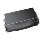
SMA (DO-214AC)
Cathode
Anode
• Meets MSL level 1, per J-STD-020, LF maximum peak
of 260 °C
• Material categorization: for definitions of compliance
please see www.vishay.com/doc?99912
ADDITIONAL RESOURCES
3D 3D
MECHANICAL DATA
3D Models
PRIMARY CHARACTERISTICS
Case: SMA (DO-214AC)
Molding compound meets UL 94 V-0 flammability rating
Base P/N-M3 - halogen-free, RoHS-compliant, and
commercial grade
IF(AV)
1.0 A
VRRM
1300 V
IFSM
18 A
Terminals: matte tin plated leads, solderable
J-STD-002 and JESD 22-B102
M3 suffix meets JESD 201 class 2 whisker test
trr
75 ns
Polarity: color band denotes the cathode end
ER
5 mJ
VF at IF = 1.0 A (TA = 125 °C)
1.39 V
TJ max.
150 °C
Package
SMA (DO-214AC)
Circuit configurations
Single
per
TYPICAL APPLICATIONS
For use in high voltage, high frequency rectification specially
suited for freewheeling, clamping, snubbering in power
supply, ignition drive of HID, UHP and industrial ballast and
snubber for PDP TV power supply application.
MAXIMUM RATINGS (TC = 25 °C unless otherwise noted)
PARAMETER
SYMBOL
Device marking code
BYG23T
UNIT
BYG23T
1300
V
Maximum DC forward current (fig.1)
IF
(1)
1.0
A
Peak forward surge current 8.3 ms single half sine-wave
superimposed on rated load
IFSM
18
A
Pulse energy in avalanche mode, non repetitive
(inductive load switch off) I(BR)R = 0.4 A, TL = 25 °C
ER
5
mJ
Maximum operating junction temperature
TJ
150
°C
TSTG
-55 to +150
°C
Maximum repetitive peak reverse voltage
Storage temperature range
VRRM
Note
• Free air, mounted on recommended copper pad area
Revision: 25-Feb-2020
Document Number: 89429
1
For technical questions within your region: DiodesAmericas@vishay.com, DiodesAsia@vishay.com, DiodesEurope@vishay.com
THIS DOCUMENT IS SUBJECT TO CHANGE WITHOUT NOTICE. THE PRODUCTS DESCRIBED HEREIN AND THIS DOCUMENT
ARE SUBJECT TO SPECIFIC DISCLAIMERS, SET FORTH AT www.vishay.com/doc?91000
�BYG23T-M3
www.vishay.com
Vishay General Semiconductor
ELECTRICAL CHARACTERISTICS (TC = 25 °C unless otherwise noted)
PARAMETER
TEST CONDITIONS
SYMBOL
TA = 25 °C
Instantaneous forward voltage (1)
IF = 1.0 A
Reverse current (2)
VR = 1300 V
Maximum reverse recovery time
IF = 0.5 A, IR = 1.0 A, Irr = 0.25 A
Forward recovery time
Peak forward voltage
IF = 1.5 A, dI/dt = 12 A/μs,
VF = 1.1 x VF max.
Typical junction capacitance
4.0 V, 1 MHz
VF
TA = 125 °C
TA = 25 °C
TA = 25 °C
TA = 25 °C
MAX.
1.74
1.9
1.39
1.65
UNIT
V
-
5.0
2.9
50
trr
65
75
tfr
620
-
VFP
9.0
-
V
CJ
9.0
-
pF
IR
TA = 125 °C
TYP.
μA
ns
Notes
(1) Pulse test: 300 μs pulse width, 1 % duty cycle
(2) Pulse test: Pulse width ≤ 40 ms
THERMAL CHARACTERISTICS (TA = 25 °C unless otherwise noted)
PARAMETER
SYMBOL
BYG23T
RθJA
120
RθJM
20
Typical thermal resistance (1)
UNIT
°C/W
Note
(1) Free air, mounted on recommended PCB 1 oz. pad area. Thermal resistance R
θJA - junction to ambient, RθJM - junction to mount
ORDERING INFORMATION (Example)
PREFERRED P/N
UNIT WEIGHT (g)
PREFERRED PACKAGE CODE
BASE QUANTITY
DELIVERY MODE
BYG23T-M3/TR
0.064
TR
1800
7" diameter plastic tape and reel
BYG23T-M3/TR3
0.064
TR3
7500
13" diameter plastic tape and reel
Revision: 25-Feb-2020
Document Number: 89429
2
For technical questions within your region: DiodesAmericas@vishay.com, DiodesAsia@vishay.com, DiodesEurope@vishay.com
THIS DOCUMENT IS SUBJECT TO CHANGE WITHOUT NOTICE. THE PRODUCTS DESCRIBED HEREIN AND THIS DOCUMENT
ARE SUBJECT TO SPECIFIC DISCLAIMERS, SET FORTH AT www.vishay.com/doc?91000
�BYG23T-M3
www.vishay.com
Vishay General Semiconductor
RATINGS AND CHARACTERISTICS CURVES (TA = 25 °C unless otherwise noted)
Axis Title
1.2
0.8
0.6
0.4
TM - Measured
at the Lead terminal
0.2
0
0
25
50
75
100
125
150
Tj = 150 °C
10
Tj = 125 °C
1000
1
Tj = 25 °C
0.1
100
0.01
Tj = -40 °C
0.001
10
0.0001
175
10
TM - Mount Temperature (°C)
Junction Capacitance (pF)
Average Power Loss (W)
D = 0.2
D = 1.0
D = 0.1
1.0
0.8
T
0.6
0.4
0.2
D = tp/T
0.1
1
1000
Tj = 25 °C
1
100
Tj = -40 °C
0.1
10
2.4
2.8
3.2
3.6
4.0
Instantaneous Forward Voltage (V)
Fig. 3 - Typical Instantaneous Forward Characteristics
Transient Thermal Impedance (°C/W)
Instantaneous Forward Current (A)
2nd line
Tj = 150 °C
2.0
10
100
Fig. 5 - Typical Junction Capacitance
10
1.6
100
Reverse Voltage (V)
10000
1.2
90
10
Fig. 2 - Forward Power Loss Characteristics
0.8
80
TJ = 25 °C
f = 1.0 MHz
Vstg = 50 mVp-p
Average Forward Current (A)
0.4
70
1
0.1 0.2 0.3 0.4 0.5 0.6 0.7 0.8 0.9 1.0 1.1 1.2
Tj = 125 °C
60
tp
0
0
50
D = 0.8
1.4
1.2
40
Fig. 4 - Typical Reverse Characteristics
D = 0.3
1.6
30
100
D = 0.5
1.8
20
Percent of Rated Peak Reverse Voltage (%)
Fig. 1 - Max. Forward Current Derating Curve
2.0
1st line
2nd line
2nd line
Instantaneous Reverse Current (µA)
1.0
DC Forward Current (A)
10000
100
1000
Junction to Ambient
100
10
1
0.01
0.1
1
10
100
t - Pulse Duration (s)
Fig. 6 - Typical Transient Thermal Impedance
Revision: 25-Feb-2020
Document Number: 89429
3
For technical questions within your region: DiodesAmericas@vishay.com, DiodesAsia@vishay.com, DiodesEurope@vishay.com
THIS DOCUMENT IS SUBJECT TO CHANGE WITHOUT NOTICE. THE PRODUCTS DESCRIBED HEREIN AND THIS DOCUMENT
ARE SUBJECT TO SPECIFIC DISCLAIMERS, SET FORTH AT www.vishay.com/doc?91000
�BYG23T-M3
www.vishay.com
Vishay General Semiconductor
PACKAGE OUTLINE DIMENSIONS in inches (millimeters)
SMA (DO-214AC)
Cathode Band
Mounting Pad Layout
0.110 (2.79)
0.100 (2.54)
0.065 (1.65)
0.049 (1.25)
0.177 (4.50)
0.157 (3.99)
0.012 (0.305)
0.006 (0.152)
0.060 (1.52)
MIN.
0.208 (5.28)
REF.
0.090 (2.29)
0.078 (1.98)
0.060 (1.52)
0.030 (0.76)
0.074 (1.88)
MAX.
0.066 (1.68)
MIN.
0.008 (0.203)
0 (0)
0.208 (5.28)
0.194 (4.93)
Revision: 25-Feb-2020
Document Number: 89429
4
For technical questions within your region: DiodesAmericas@vishay.com, DiodesAsia@vishay.com, DiodesEurope@vishay.com
THIS DOCUMENT IS SUBJECT TO CHANGE WITHOUT NOTICE. THE PRODUCTS DESCRIBED HEREIN AND THIS DOCUMENT
ARE SUBJECT TO SPECIFIC DISCLAIMERS, SET FORTH AT www.vishay.com/doc?91000
�Legal Disclaimer Notice
www.vishay.com
Vishay
Disclaimer
ALL PRODUCT, PRODUCT SPECIFICATIONS AND DATA ARE SUBJECT TO CHANGE WITHOUT NOTICE TO IMPROVE
RELIABILITY, FUNCTION OR DESIGN OR OTHERWISE.
Vishay Intertechnology, Inc., its affiliates, agents, and employees, and all persons acting on its or their behalf (collectively,
“Vishay”), disclaim any and all liability for any errors, inaccuracies or incompleteness contained in any datasheet or in any other
disclosure relating to any product.
Vishay makes no warranty, representation or guarantee regarding the suitability of the products for any particular purpose or
the continuing production of any product. To the maximum extent permitted by applicable law, Vishay disclaims (i) any and all
liability arising out of the application or use of any product, (ii) any and all liability, including without limitation special,
consequential or incidental damages, and (iii) any and all implied warranties, including warranties of fitness for particular
purpose, non-infringement and merchantability.
Statements regarding the suitability of products for certain types of applications are based on Vishay's knowledge of typical
requirements that are often placed on Vishay products in generic applications. Such statements are not binding statements
about the suitability of products for a particular application. It is the customer's responsibility to validate that a particular product
with the properties described in the product specification is suitable for use in a particular application. Parameters provided in
datasheets and / or specifications may vary in different applications and performance may vary over time. All operating
parameters, including typical parameters, must be validated for each customer application by the customer's technical experts.
Product specifications do not expand or otherwise modify Vishay's terms and conditions of purchase, including but not limited
to the warranty expressed therein.
Hyperlinks included in this datasheet may direct users to third-party websites. These links are provided as a convenience and
for informational purposes only. Inclusion of these hyperlinks does not constitute an endorsement or an approval by Vishay of
any of the products, services or opinions of the corporation, organization or individual associated with the third-party website.
Vishay disclaims any and all liability and bears no responsibility for the accuracy, legality or content of the third-party website
or for that of subsequent links.
Except as expressly indicated in writing, Vishay products are not designed for use in medical, life-saving, or life-sustaining
applications or for any other application in which the failure of the Vishay product could result in personal injury or death.
Customers using or selling Vishay products not expressly indicated for use in such applications do so at their own risk. Please
contact authorized Vishay personnel to obtain written terms and conditions regarding products designed for such applications.
No license, express or implied, by estoppel or otherwise, to any intellectual property rights is granted by this document or by
any conduct of Vishay. Product names and markings noted herein may be trademarks of their respective owners.
© 2022 VISHAY INTERTECHNOLOGY, INC. ALL RIGHTS RESERVED
Revision: 01-Jan-2022
1
Document Number: 91000
�


 工商网监
湘ICP备2023018690号
工商网监
湘ICP备2023018690号
