DG9424E, DG9425E, DG9426E
www.vishay.com
Vishay Siliconix
1.6 On Resistance, ± 5 V, +12 V, and +3 V Quad SPST Switches
DESCRIPTION
FEATURES
The DG9424E, DG9425E, DG9426E are monolithic quad
single-pole-single-throw analog switches. The G9424E and
DG9425E differ only in that they respond to opposite logic
levels. The DG9426E has two normally open and two
normally closed switches. It can be given various
configurations, including four SPST, two SPDT, and one
DPDT.
• 3 V to 16 V single supply or ± 3 V thru ± 8 V dual supply
operation
• 1.6 typical on resistance
• 3 V logic compatible for control
• Bidirectional rail to rail signal switching
• Fast switching speed
Using BiCMOS wafer fabrication technology allows the
DG9424E, DG9425E, and DG9426E to operate on single
and dual supplies. Single supply voltage ranges from 3 V to
16 V while dual supply operation is recommended with
± 3 V to ± 8 V. Each switch conducts equally well in both
direction when on, and blocks input voltages up to the
supply levels when off.
• < 0.2 nA switch on leakage
The low and flat on resistance over the full input signal
voltage rang bring excellent linearity, reduce insertion loss
and signal distortion, make them ideal for data acquisition
and programmable gain control applications. These switch
characters also make them ideal fit for audio signal switch
and reed relay replacement.
• Fast switching time
• Break-before-make switching - DG9426
BENEFITS
• Wide operation voltage range
• Low signal errors and distortion
• Simple interfacing
APPLICATIONS
• Automatic test equipment
• Data acquisition systems
The DG9424E, DG9425E, DG9426E feature low power
dissipation, fast switching speed, and low voltage logic
control threshold. Proprietary design enables the low charge
injection that minimize the switching transient.
• Meters and instruments
• Medical and healthcare systems
• Communication systems
Operation temperature is specified from -40 °C to +85 °C.
The DG9424E, DG9425E, DG9426E are available in 16 lead
TSSOP packages.
• Audio and video signal routing
• Relay replacement
• Battery powered systems
• Computer peripherals
• Audio and video signal routing
FUNCTIONAL BLOCK DIAGRAM AND PIN CONFIGURATION
S1
1
V-
2
D1
IN1
IN2
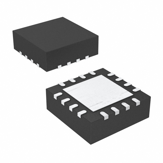
D2
QFN-16 (4 mm x 4 mm)
16
15
14
13
12
S2
11
V+
Top View
S4
4
9
S3
5
6
7
8
D3
VL
IN3
10
IN4
3
D4
GND
Note
• QFN exposed pad can either be tied to V- or left floating
S20-0477-Rev. C, 22-Jun-2020
Document Number: 75770
1
For technical questions, contact: analogswitchtechsupport@vishay.com
THIS DOCUMENT IS SUBJECT TO CHANGE WITHOUT NOTICE. THE PRODUCTS DESCRIBED HEREIN AND THIS DOCUMENT
ARE SUBJECT TO SPECIFIC DISCLAIMERS, SET FORTH AT www.vishay.com/doc?91000
�DG9424E, DG9425E, DG9426E
www.vishay.com
Vishay Siliconix
FUNCTIONAL BLOCK DIAGRAM AND PIN CONFIGURATION
DG9426E
DG9424E / DG9425E
TSSOP
TSSOP
IN1
1
16
IN2
COM1
2
15
COM2
NC1
3
14
NO2
V+
V-
4
13
V+
12
VL
GND
5
12
VL
6
11
NC3/NO3
NC4
6
11
NO3
7
10
COM3
COM4
7
10
COM3
8
9
IN3
IN4
8
9
IN3
IN1
1
16
IN2
COM1
2
15
COM2
NC1/NO1
3
14
NC2/NO2
V-
4
13
GND
5
NC4/NO4
COM4
IN4
Top View
Top View
TRUTH TABLE
TRUTH TABLE
LOGIC
DG9424E
DG9425E
LOGIC
SW1, SW4
SW2, SW3
0
Off
On
0
On
Off
1
On
Off
1
Off
On
ORDERING INFORMATION
TEMP. RANGE
PACKAGE
16-pin TSSOP
-40 °C to +85 °C
QFN (4 mm x 4 mm) 16L
(variation 2)
PART NUMBER
PART MARKING
STD PACK QUANTITY
DG9424EDQ-T1-GE3
9424E
Tape and reel 3000 units
DG9425EDQ-T1-GE3
9425E
Tape and reel 3000 units
DG9426EDQ-T1-GE3
9426E
Tape and reel 3000 units
DG9424EDN-T1-GE4
9424E
Tape and reel 2500 units
DG9425EDN-T1-GE4
9425E
Tape and reel 2500 units
DG9426EDN-T1-GE4
9426E
Tape and reel 2500 units
ABSOLUTE MAXIMUM RATINGS
PARAMETER
LIMIT
V+ to VGND to V-
18
VL
(GND - 0.3) to (V+) + 0.3
IN, COM, NC, NO a
100
Peak current, S or D (pulsed 1 ms, 10 % duty cycle)
200
Storage temperature
Thermal resistance b
16-pin TSSOP c
ESD human body model (HBM); per ANSI / ESDA / JEDEC® JS-001
Latch up current, per JESD78D
V
(V-) - 0.3 to (V+) + 0.3
Continuous current (NO, NC, COM pins)
Power dissipation (package) b
UNIT
-0.3 to +18
mA
-65 to +150
°C
450
mW
178
°C/W
>1500
V
400
mA
Notes
a. Signals on NC, NO, COM or IN exceeding V+ or V- will be clamped by internal diodes. Limit forward diode current to maximum current
ratings
b. All leads welded or soldered to PC board
c. Derate 7 mW/°C above 25 °C
Stresses beyond those listed under “Absolute Maximum Ratings” may cause permanent damage to the device. These are stress ratings only, and functional operation
of the device at these or any other conditions beyond those indicated in the operational sections of the specifications is not implied. Exposure to absolute maximum
rating conditions for extended periods may affect device reliability.
S20-0477-Rev. C, 22-Jun-2020
Document Number: 75770
2
For technical questions, contact: analogswitchtechsupport@vishay.com
THIS DOCUMENT IS SUBJECT TO CHANGE WITHOUT NOTICE. THE PRODUCTS DESCRIBED HEREIN AND THIS DOCUMENT
ARE SUBJECT TO SPECIFIC DISCLAIMERS, SET FORTH AT www.vishay.com/doc?91000
�DG9424E, DG9425E, DG9426E
www.vishay.com
SPECIFICATIONS
a
Vishay Siliconix
Single Supply 12 V
PARAMETER
SYMBOL
TEST CONDITIONS UNLESS
OTHERWISE SPECIFIED
V+ = 12 V, V- = 0 V
VL = 5 V, VIN = 2.4 V, 0.8 V f
LIMITS
-40 °C to +85 °C
TEMP. b
MIN. d
UNIT
TYP. c
MAX. d
Analog Switch
Analog signal range e
On-resistance
VANALOG
RON
V+ = 10.8 V, V- = 0 V,
INO, INC = 50 mA, VCOM = 2/9 V
Full
0
-
12
V
Room
-
1.6
3
Full
-
-
4
Full
-1
0.01
1
Room
-
36
51
Full
-
-
65
Room
-
20
35
Full
-
-
44
-
-
Digital Control
Input current
IINL or IINH
μA
Dynamic Characteristics
Turn-on time e
tON
Turn-off time e
tOFF
RL = 300 , CL = 35 pF,
VNO, VNC = 5 V, see Fig. 2
tD
DG9426E only, VNO, VNC = 5 V,
RL = 300 , CL = 35 pF
Room
2
Charge injection e
QINJ
Vg = 0 V, Rg = 0 , CL = 1 nF
Room
-
38
-
Off-isolation e
OIRR
Room
-
-56
-
Channel-to-channel crosstalk e
XTALK
RL = 50 , CL = 5 pF,
f = 1 MHz
Room
-
-77
-
Room
-
49
-
Room
-
37
-
Room
-
89
-
Room
-
0.02
1
Full
-
-
5
Room
-1
-0.002
-
Full
-5
-
-
Room
-
0.002
1
Break-before-make time delay e
NO, NC off capacitance e
CNO(off)
CNC(off)
COM off capacitance e
CCOM(off)
Channel on capacitance e
CCOM(on)
f = 1 MHz
ns
pC
dB
pF
Power Supplies
Positive supply current
Negative supply current
I+
IVIN = 0 or VL
Logic supply current
Ground current
S20-0477-Rev. C, 22-Jun-2020
IL
IGND
Full
-
-
5
Room
-1
-0.002
-
Full
-5
-
-
μA
Document Number: 75770
3
For technical questions, contact: analogswitchtechsupport@vishay.com
THIS DOCUMENT IS SUBJECT TO CHANGE WITHOUT NOTICE. THE PRODUCTS DESCRIBED HEREIN AND THIS DOCUMENT
ARE SUBJECT TO SPECIFIC DISCLAIMERS, SET FORTH AT www.vishay.com/doc?91000
�DG9424E, DG9425E, DG9426E
www.vishay.com
SPECIFICATIONS
a
Vishay Siliconix
Dual Supply ± 5 V
PARAMETER
SYMBOL
TEST CONDITIONS UNLESS
OTHERWISE SPECIFIED
V+ = 5 V, V- = 5 V
VL = 5 V, VIN = 2.4 V, 0.8 V f
LIMITS
-40 °C to +85 °C
TEMP.b
MIN. d
UNIT
TYP. c
MAX. d
Analog Switch
Analog signal range e
On-resistance
VANALOG
RON
V+ = 4.5 V, V- = -4.5 V,
INO, INC = 50 mA
INO(off)
Switch off leakage current
INC(off)
ICOM(off)
Channel on leakage current
ICOM(on)
V+ = 5.5 V, V- = -5.5 V,
VCOM = ± 4.5 V, VNO, VNC = ± 4.5 V
V+ = 5.5 V, V- = -5.5 V,
VNO, VNC = VCOM = ± 4.5 V
Full
-5
5
V
Room
-
1.9
3.3
Full
-
-
4.3
Room
-1
-
1
Full
-10
-
10
Room
-1
-
1
Full
-10
-
10
Room
-1
-
1
Full
-10
-
10
Full
-1
0.05
1
Room
-
48
67
Full
-
-
81
Room
-
34
57
Full
-
-
67
Room
2
-
-
nA
Digital Control
Input current a
IINL or IINH
μA
Dynamic Characteristics
Turn-on time e
tON
Turn-off time e
tOFF
RL = 300 , CL = 35 pF,
VNO, VNC = ± 3.5 V, see Fig. 2
tD
DG9426E only, VNO, VNC = 3.5 V,
RL = 300 , CL = 35 pF
Charge injection e
QINJ
Vg = 0 V, Rg = 0 , CL = 1 nF
Off isolation e
OIRR
Channel-to-channel crosstalk e
XTALK
Break-before-make time delay e
Source off capacitance e
CNO(off)
CNC(off)
Drain off capacitance e
CCOM(off)
Channel on capacitance e
CCOM(on)
RL = 50 , CL = 5 pF, f = 1 MHz
f = 1 MHz
Room
-
112
-
Room
-
-56
-
Room
-
-82
-
Room
-
38
-
Room
-
38
-
Room
-
89
-
Room
-
0.03
1
Full
-
-
5
Room
-1
-0.002
-
Full
-5
-
-
Room
-
0.002
1
Full
-
-
5
Room
-1
-0.002
-
Full
-5
-
-
ns
pC
dB
pF
Power Supplies
Positive supply current e
I+
Negative supply current e
I-
Logic supply current e
IL
VIN = 0 or VL
Ground current e
S20-0477-Rev. C, 22-Jun-2020
IGND
μA
Document Number: 75770
4
For technical questions, contact: analogswitchtechsupport@vishay.com
THIS DOCUMENT IS SUBJECT TO CHANGE WITHOUT NOTICE. THE PRODUCTS DESCRIBED HEREIN AND THIS DOCUMENT
ARE SUBJECT TO SPECIFIC DISCLAIMERS, SET FORTH AT www.vishay.com/doc?91000
�DG9424E, DG9425E, DG9426E
www.vishay.com
SPECIFICATIONS
a
Vishay Siliconix
Single Supply 5 V
PARAMETER
SYMBOL
TEST CONDITIONS UNLESS
OTHERWISE SPECIFIED
V+ = 5 V, V- = 0 V
VL = 5 V, VIN = 2.4 V, 0.8 V f
LIMITS
-40 °C to +85 °C
TEMP. b
MIN. d
TYP. c
UNIT
MAX. d
Analog Switch
Analog signal range e
On-resistance e
VANALOG
RON
V+ = 4.5 V, INO, INC = 50 mA
Full
-
-
5
V
Room
-
3.1
4.8
Full
-
-
5.8
Room
-
62
78
Hot
-
-
106
Room
-
29
44
Hot
-
-
56
Dynamic Characteristics
Turn-on time e
tON
Turn-off time e
tOFF
Break-before-make time delay e
Charge injection e
RL = 300 , CL = 35 pF,
VNO, VNC = 3.5 V, see Fig. 2
tD
DG9426E only, VNO, VNC = 3.5 V,
RL = 300 , CL = 35 pF
Room
5
-
-
QINJ
Vg = 0 V, Rg = 0 , CL = 1 nF
Room
-
10
-
Room
-
0.02
1
Hot
-
-
5
Room
-1
-0.002
-
Hot
-5
-
-
Room
-
0.002
1
ns
pC
Power Supplies
Positive supply current e
Negative supply current e
I+
IVIN = 0 or VL
Logic supply current e
Ground current e
S20-0477-Rev. C, 22-Jun-2020
IL
IGND
Hot
-
-
5
Room
-1
-0.002
-
Hot
-5
-
-
μA
Document Number: 75770
5
For technical questions, contact: analogswitchtechsupport@vishay.com
THIS DOCUMENT IS SUBJECT TO CHANGE WITHOUT NOTICE. THE PRODUCTS DESCRIBED HEREIN AND THIS DOCUMENT
ARE SUBJECT TO SPECIFIC DISCLAIMERS, SET FORTH AT www.vishay.com/doc?91000
�DG9424E, DG9425E, DG9426E
www.vishay.com
SPECIFICATIONS
a
Vishay Siliconix
Single Supply 3 V
PARAMETER
SYMBOL
TEST CONDITIONS UNLESS
OTHERWISE SPECIFIED
V+ = 3 V, V- = 0 V
VL = 3 V, VIN = 2.4 V, 0.4 V f
LIMITS
-40 °C to +85 °C
TEMP.b
MIN. d
UNIT
TYP. c
MAX. d
Analog Switch
Analog signal range e
On-resistance
Switch off leakage current a
VANALOG
RON
Full
0
-
3
V
Room
-
6
-
Full
-
-
-
INO(off)
Room
-1
-
1
INC(off)
Full
-10
-
10
Room
-1
-
1
Full
-10
-
10
ICOM(off)
Channel on leakage current a
V+ = 2.7 V, V- = 0 V.
INO, INC = 5 mA, VCOM = 0.5, 2.2 V
ICOM(on)
V+ = 3.3 V, V- = 0 V.
VCOM = 0.3, 3 V, VNO, VNC = 3, 0.3 V
V+ = 3.3 V, V- = 0 V,
VNO, VNC = VCOM = 0.3, 3 V
Room
-1
-
1
Full
-10
-
10
Full
-1
0.005
1
Room
-
140
-
Full
-
-
193
Room
-
65
-
Full
-
-
89
Room
5
nA
Digital Control e
Input current
IINL or IINH
μA
Dynamic Characteristics
Turn-on time
tON
Turn-off time
tOFF
RL = 300 , CL = 35 pF.
VNO, VNC = 1.5 V, see Fig. 2
tD
DG9426E only, VNO, VNC = 1.5 V,
RL = 300 , CL = 35 pF
Charge injection e
QINJ
Vg = 0 V, Rg = 0 , CL = 1 nF
Room
-
15
-
Off isolation e
OIRR
-
-56
-
Channel-to-channel crosstalk e
XTALK
RL = 50 , CL = 5 pF,
f = 1 MHz
Room
Room
-
-80
-
Room
-
53
-
Room
-
42
-
Room
-
92
-
Break-before-make time delay
Source off capacitance e
CNO(off)
CNC(off)
Drain off capacitance e
CCOM(off)
Channel on capacitance e
CCOM(on)
f = 1 MHz
ns
pC
dB
pF
Notes
a. Leakage parameters are guaranteed by worst case test conditions and not subject to production test
b. Room = 25 °C, Full = As determined by the operating temperature suffix
c. Typical values are for DESIGN AID ONLY, not guaranteed nor subject to production testing
d. The algebraic convention whereby the most negative value is a minimum and the most positive a maximum, is used in this datasheet
e. Guaranteed by design, not subject to production test
f. VIN = Input voltage to perform proper function
S20-0477-Rev. C, 22-Jun-2020
Document Number: 75770
6
For technical questions, contact: analogswitchtechsupport@vishay.com
THIS DOCUMENT IS SUBJECT TO CHANGE WITHOUT NOTICE. THE PRODUCTS DESCRIBED HEREIN AND THIS DOCUMENT
ARE SUBJECT TO SPECIFIC DISCLAIMERS, SET FORTH AT www.vishay.com/doc?91000
�DG9424E, DG9425E, DG9426E
www.vishay.com
Vishay Siliconix
TYPICAL CHARACTERISTICS (25 °C, unless otherwise noted)
10
12
TA = 25 °C
IS = -1 mA
V+ = 2.7V, V- = 0V
9
10
RON - On-Resistance ()
RON - On-Resistance ()
8
V+ = 4.5V, V- = 0V
7
6
V+ = 7.2V, V- = 0V
5
V+ = 10.8V, V- = 0V
4
V+ = 14.4V, V- = 0V
3
V+/- = 2.7/0 V
IS = 50 mA
2
+85 °C
8
6
4
-40 °C
+25 °C
2
1
0
0
0
2
4
6
8
10
12
14
16
0
1
VCOM - Analog Voltage (V)
RON vs. VCOM and Supply Voltage
120
V+ = ± 5 V
Is = 50 mA
110
tON(EN), tOFF(EN) - Switching Time (ns)
7
RON - On-Resistance ( )
3
RON vs. Analog Voltage and Temperature
8
6
5
4
+85C
3
2
1
-40C
VSUPPLY = ± 5V
100
90
80
70
tON Vs = -3.5 V
tOFF Vs = -3.5 V
60
tON Vs = +3.5 V
50
tOFF Vs = +3.5 V
40
30
20
10
+25C
0
0
-5
-4
-3
-2
-1
0
1
2
3
4
5
-60 -40 -20
0
20
40
60
80
100 120 140
VCOM - Analog Voltage (V)
Temperature (°C)
RON vs. Analog Voltage and Temperature
Switching Time vs. Temperature and Dual Supply Voltage
200.0
180
tON V+ = 3 V
150
120
tON V+ = 5 V
tOFF V+ = 3 V
tON V+ = 12 V
90
tOFF V+ = 5 V
60
V+ = 5 V
V- = -5 V
150.0
tOFF V+ = 12 V
Leakage Current (pA)
tON(EN), tOFF(EN) - Switching Time (ns)
2
VCOM - Analog Voltage (V)
100.0
50.0
0
-50.0
-100.0
30
-150.0
-200.0
0
-40
-20
0
20
40
60
80
100
120
Temperature (°C)
Switching Time vs. Temperature and Single Supply Voltage
S20-0477-Rev. C, 22-Jun-2020
-5
-4
-3
-2
-1
0
1
2
3
4
5
VCOM, VNO, VNC - Analog Voltage (V)
Leakage Current vs. Analog Voltage
Document Number: 75770
7
For technical questions, contact: analogswitchtechsupport@vishay.com
THIS DOCUMENT IS SUBJECT TO CHANGE WITHOUT NOTICE. THE PRODUCTS DESCRIBED HEREIN AND THIS DOCUMENT
ARE SUBJECT TO SPECIFIC DISCLAIMERS, SET FORTH AT www.vishay.com/doc?91000
�DG9424E, DG9425E, DG9426E
www.vishay.com
Vishay Siliconix
TYPICAL CHARACTERISTICS (25 °C, unless otherwise noted)
5.0
100,000
V+ = +5.5 V
V- = -5.5 V
4.0
ID(ON)
ID(OFF)
1,000
IS(OFF)
100
10
VT - Switching Threshold (V)
10,000
Leakage Current (pA)
-40 °C to +85 °C
VL = V+
4.5
3.5
3.0
VINH
2.5
VINL
2.0
1.5
1.0
0.5
0
1
-60 -40 -20
0
20
40
60
80
2
100 120 140
4
Temperature (°C)
12
14
10
V+ = +5 V
V- = -5 V
0
Insertion Loss
-10
-20
Loss, OIRR, XTALK (dB)
1000
100
10
1
0.1
-30
-40
-50
Off Isolation
-60
Crosstalk
-70
-80
V+ = 3 V
V- = 0 V
RL = 50
-90
0.01
0.001
10
10
Switching Threshold vs. Supply Voltage
100000
I+ - Supply Current (μA)
8
V+ - Supply Voltage (V)
Leakage Current vs. Temperature
10000
6
-100
100
1000
10K
100K
1M
10M
Input Switching Frequency (Hz)
Switching Current vs. Input Switching Frequency
S20-0477-Rev. C, 22-Jun-2020
-110
100K
1M
10M
100M
1G
Frequency (Hz)
Insertion Loss, Off Isolation and Crosstalk vs. Frequency
Document Number: 75770
8
For technical questions, contact: analogswitchtechsupport@vishay.com
THIS DOCUMENT IS SUBJECT TO CHANGE WITHOUT NOTICE. THE PRODUCTS DESCRIBED HEREIN AND THIS DOCUMENT
ARE SUBJECT TO SPECIFIC DISCLAIMERS, SET FORTH AT www.vishay.com/doc?91000
�DG9424E, DG9425E, DG9426E
www.vishay.com
Vishay Siliconix
SCHEMATIC DIAGRAM (typical channel)
V+
S
VL
Level
Shift/
Drive
VIN
D
GND
V-
Fig. 1
TEST CIRCUITS
VL
V+
tr < 5 ns
tf < 5 ns
VINH
Logic
Input
50 %
VINL
VL
VIN
V+
NO or NC
tOFF
COM
VOUT
VOUT
IN
RL
300 Ω
V-
GND
CL
35 pF
0.9 x VOUT
90 %
0V
Switch
Output
tON
Switch
VCL (includes fixture and stray capacitance)
VOUT = VIN
RL
Note:
RL + rON
Logic input waveform is inverted for switches that
have the opposite logic sense control
Fig. 2 - Switching Time
VL
V+
Logic
Input
VIN1
NO1
COM1
VIN2
Switch
Output
IN2
RL1
300 Ω
V-
GND
90 %
VO2
COM2
NC2
50 %
0V
VIN1
VO1
VO1
IN1
3V
RL2
300 Ω
CL2
35 pF
CL1
35 pF
Switch
Output
0V
VIN2
VO2
0V
90 %
tD
tD
VCL (includes fixture and stray capacitance)
Fig. 3 - Break-Before-Make (DG9426E)
S20-0477-Rev. C, 22-Jun-2020
Document Number: 75770
9
For technical questions, contact: analogswitchtechsupport@vishay.com
THIS DOCUMENT IS SUBJECT TO CHANGE WITHOUT NOTICE. THE PRODUCTS DESCRIBED HEREIN AND THIS DOCUMENT
ARE SUBJECT TO SPECIFIC DISCLAIMERS, SET FORTH AT www.vishay.com/doc?91000
�DG9424E, DG9425E, DG9426E
www.vishay.com
Vishay Siliconix
TEST CIRCUITS
VL
ΔVO
V+
VO
VL
Rg
V+
COM
INX
NO or NC
IN
Vg
OFF
VOUT
ON
OFF
CL
10 nF
V-
GND
INX
V-
OFF
ON
Q = ΔVO x CL
OFF
INX dependent on switch configuration Input polarity determined
by sense of switch.
VIN = 0 - V+
Fig. 4 - Charge Injection
C
VL
VL
NO1
VS
Rg = 50 Ω
V+
C
V+
COM1
50 Ω
IN1
0 V, 2.4 V
NO2
COM2
VOUT
NC
0 V, 2.4 V
RL
IN2
GND
XTALK Isolation = 20 log
V-
C
VOUT
VIN
V-
C = RF bypass
Fig. 5 - Crosstalk
VL
V+
VL
C
V+
C
C
VIN
VL
NO or NC
V+
C
VOUT
COM
VL
0 V, 2.4 V
V+
COM
Rg = 50 Ω
RL
50 Ω
IN
GND
V-
C
Meter
IN
HP4192A
Impedance
Analyzer
or Equivalent
0 V, 2.4 V
NO or NC
GND
VOff Isolation = 20 log
V-
C
VOUT
VIN
V-
C = RF Bypass
Fig. 6 - Off-Isolation
Fig. 7 - Source/Drain Capacitances
Vishay Siliconix maintains worldwide manufacturing capability. Products may be manufactured at one of several qualified locations. Reliability data for Silicon
Technology and Package Reliability represent a composite of all qualified locations. For related documents such as package / tape drawings, part marking, and
reliability data, see www.vishay.com/ppg?75770.
S20-0477-Rev. C, 22-Jun-2020
Document Number: 75770
10
For technical questions, contact: analogswitchtechsupport@vishay.com
THIS DOCUMENT IS SUBJECT TO CHANGE WITHOUT NOTICE. THE PRODUCTS DESCRIBED HEREIN AND THIS DOCUMENT
ARE SUBJECT TO SPECIFIC DISCLAIMERS, SET FORTH AT www.vishay.com/doc?91000
�Package Information
www.vishay.com
Vishay Siliconix
QFN 4x4-16L Case Outline
(5)
(4)
VARIATION 1
MILLIMETERS(1)
DIM
VARIATION 2
MILLIMETERS(1)
INCHES
INCHES
MIN.
NOM.
MAX.
MIN.
NOM.
MAX.
MIN.
NOM.
MAX.
MIN.
NOM.
MAX.
A
0.75
0.85
0.95
0.029
0.033
0.037
0.75
0.85
0.95
0.029
0.033
0.037
A1
0
-
0.05
0
-
0.002
0
-
0.05
0
-
0.002
0.35
0.010
0.014
0.25
0.35
0.010
2.2
0.079
0.087
2.5
2.7
0.098
A3
b
0.20 ref.
0.25
D
D2
0.30
0.008 ref.
4.00 BSC
2.0
2.1
0.012
0.20 ref.
0.157 BSC
0.083
0.30
4.00 BSC
2.6
e
0.65 BSC
0.026 BSC
0.65 BSC
E
4.00 BSC
0.157 BSC
4.00 BSC
E2
2.0
K
L
2.1
2.2
0.079
0.20 min.
0.5
0.6
0.083
0.087
2.5
0.008 min.
0.7
0.020
0.024
0.008 ref.
2.6
0.3
0.4
0.014
0.157 BSC
0.102
0.106
0.026 BSC
0.157 BSC
2.7
0.098
0.20 min.
0.028
0.012
0.102
0.106
0.008 min.
0.5
0.012
0.016
N(3)
16
16
16
16
Nd(3)
4
4
4
4
Ne(3)
4
4
4
4
0.020
Notes
(1) Use millimeters as the primary measurement.
(2) Dimensioning and tolerances conform to ASME Y14.5M. - 1994.
(3) N is the number of terminals. Nd and Ne is the number of terminals in each D and E site respectively.
(4) Dimensions b applies to plated terminal and is measured between 0.15 mm and 0.30 mm from terminal tip.
(5) The pin 1 identifier must be existed on the top surface of the package by using identification mark or other feature of package body.
(6) Package warpage max. 0.05 mm.
ECN: S13-0893-Rev. B, 22-Apr-13
DWG: 5890
Revision: 22-Apr-13
Document Number: 71921
1
For technical questions, contact: powerictechsupport@vishay.com
THIS DOCUMENT IS SUBJECT TO CHANGE WITHOUT NOTICE. THE PRODUCTS DESCRIBED HEREIN AND THIS DOCUMENT
ARE SUBJECT TO SPECIFIC DISCLAIMERS, SET FORTH AT www.vishay.com/doc?91000
�Package Information
Vishay Siliconix
TSSOP: 16-LEAD
DIMENSIONS IN MILLIMETERS
Symbols
Min
Nom
Max
A
-
1.10
1.20
A1
0.05
0.10
0.15
A2
-
1.00
1.05
0.38
B
0.22
0.28
C
-
0.127
-
D
4.90
5.00
5.10
E
6.10
6.40
6.70
E1
4.30
4.40
4.50
e
-
0.65
-
L
0.50
0.60
0.70
L1
0.90
1.00
1.10
y
-
-
0.10
θ1
0°
3°
6°
ECN: S-61920-Rev. D, 23-Oct-06
DWG: 5624
Document Number: 74417
23-Oct-06
www.vishay.com
1
�PAD Pattern
www.vishay.com
Vishay Siliconix
RECOMMENDED MINIMUM PAD FOR TSSOP-16
0.193
(4.90)
0.171
0.014
0.026
0.012
(0.35)
(0.65)
(0.30)
(4.35)
(7.15)
0.281
0.055
(1.40)
Recommended Minimum Pads
Dimensions in inches (mm)
Revision: 02-Sep-11
1
Document Number: 63550
THIS DOCUMENT IS SUBJECT TO CHANGE WITHOUT NOTICE. THE PRODUCTS DESCRIBED HEREIN AND THIS DOCUMENT
ARE SUBJECT TO SPECIFIC DISCLAIMERS, SET FORTH AT www.vishay.com/doc?91000
�Legal Disclaimer Notice
www.vishay.com
Vishay
Disclaimer
ALL PRODUCT, PRODUCT SPECIFICATIONS AND DATA ARE SUBJECT TO CHANGE WITHOUT NOTICE TO IMPROVE
RELIABILITY, FUNCTION OR DESIGN OR OTHERWISE.
Vishay Intertechnology, Inc., its affiliates, agents, and employees, and all persons acting on its or their behalf (collectively,
“Vishay”), disclaim any and all liability for any errors, inaccuracies or incompleteness contained in any datasheet or in any other
disclosure relating to any product.
Vishay makes no warranty, representation or guarantee regarding the suitability of the products for any particular purpose or
the continuing production of any product. To the maximum extent permitted by applicable law, Vishay disclaims (i) any and all
liability arising out of the application or use of any product, (ii) any and all liability, including without limitation special,
consequential or incidental damages, and (iii) any and all implied warranties, including warranties of fitness for particular
purpose, non-infringement and merchantability.
Statements regarding the suitability of products for certain types of applications are based on Vishay's knowledge of typical
requirements that are often placed on Vishay products in generic applications. Such statements are not binding statements
about the suitability of products for a particular application. It is the customer's responsibility to validate that a particular product
with the properties described in the product specification is suitable for use in a particular application. Parameters provided in
datasheets and / or specifications may vary in different applications and performance may vary over time. All operating
parameters, including typical parameters, must be validated for each customer application by the customer's technical experts.
Product specifications do not expand or otherwise modify Vishay's terms and conditions of purchase, including but not limited
to the warranty expressed therein.
Hyperlinks included in this datasheet may direct users to third-party websites. These links are provided as a convenience and
for informational purposes only. Inclusion of these hyperlinks does not constitute an endorsement or an approval by Vishay of
any of the products, services or opinions of the corporation, organization or individual associated with the third-party website.
Vishay disclaims any and all liability and bears no responsibility for the accuracy, legality or content of the third-party website
or for that of subsequent links.
Except as expressly indicated in writing, Vishay products are not designed for use in medical, life-saving, or life-sustaining
applications or for any other application in which the failure of the Vishay product could result in personal injury or death.
Customers using or selling Vishay products not expressly indicated for use in such applications do so at their own risk. Please
contact authorized Vishay personnel to obtain written terms and conditions regarding products designed for such applications.
No license, express or implied, by estoppel or otherwise, to any intellectual property rights is granted by this document or by
any conduct of Vishay. Product names and markings noted herein may be trademarks of their respective owners.
© 2021 VISHAY INTERTECHNOLOGY, INC. ALL RIGHTS RESERVED
Revision: 09-Jul-2021
1
Document Number: 91000
�


 工商网监
湘ICP备2023018690号
工商网监
湘ICP备2023018690号
