SiF902EDZ
Vishay Siliconix
Bi-Directional N-Channel 20-V (D-S) MOSFET
FEATURES
PRODUCT SUMMARY
VDS (V)
20
RDS(on) (Ω)
ID (A)
0.022 at VGS = 4.5 V
10.3
0.023 at VGS = 4.0 V
10.0
0.026 at VGS = 3.1 V
9.4
0.028 at VGS = 2.5 V
9.0
Qg (Typ.)
• Halogen-free
• TrenchFET® Power MOSFET: 2.5 V Rated
• ESD Protected: 4000 V
RoHS
COMPLIANT
9.1
APPLICATIONS
• Battery Protection Circuitry
- Cell Li-lon LiB/LiP Battery Packs
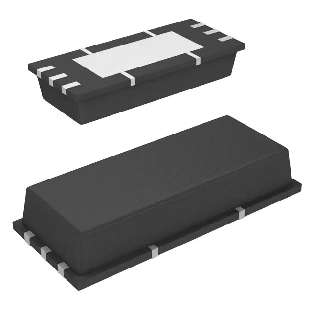
PowerPAK® 2 x 5
1
D1
S1 2 mm
S1
2
G1
3
D2
1.8 kΩ
S2
5
S2
4
G2
1.8 kΩ
G1
6
G2
Marking Code
MAXYZ
MA: Part # Code
XYZ: Lot Traceability and Date Code
S1
Ordering Information: SiF902EDZ-T1-GE3 (Lead (Pb)-free and Halogen-free)
S2
ABSOLUTE MAXIMUM RATINGS TA = 25 °C, unless otherwise noted
Parameter
Symbol
10 s
Steady State
Drain-Source Voltage
VDS
20
Gate-Source Voltage
VGS
± 12
Continuous Drain Current (TJ = 150 °C)a
TA = 25 °C
TA = 85 °C
Pulsed Drain Current (VGS = 8 V)
IS
TA = 25 °C
TA = 85 °C
PD
7.0
7.4
5.1
40
3.1
1.5
3.5
1.6
1.8
0.86
TJ, Tstg
Operating Junction and Storage Temperature Range
V
10.3
IDM
Continuous Diode Current (Diode Conduction)a
Maximum Power Dissipationa
ID
Unit
- 55 to 150
A
W
°C
THERMAL RESISTANCE RATINGS
Parameter
Maximum Junction-to-Ambienta
Maximum Junction-to-Case (Drain)
Symbol
t ≤ 10 s
Steady State
Steady State
RthJA
RthJC
Typical
Maximum
30
36
61
76
4.8
6.0
Unit
°C/W
Notes:
a. Surface Mounted on 1" x 1" FR4 board.
Document Number: 72987
S-80643-Rev. B, 24-Mar-08
www.vishay.com
1
�SiF902EDZ
Vishay Siliconix
SPECIFICATIONS TJ = 25 °C, unless otherwise noted
Parameter
Symbol
Test Conditions
Min.
VGS(th)
VDS = VGS, ID = 250 µA
0.6
Typ.
Max.
Unit
1.5
V
Static
Gate Threshold Voltage
Gate-Body Leakage
IGSS
Zero Gate Voltage Drain Current
IDSS
a
Drain-Source On-State Resistancea
Forward Transconductance
Diode Forward Voltage
a
± 500
VDS = 20 V, VGS = 0 V
1
µA
5
VDS = 5 V, VGS = 4.5 V
RDS(on)
a
± 10
VDS = 0 V, VGS = ± 12 V
VDS = 20 V, VGS = 0 V, TJ = 85 °C
ID(on)
On-State Drain Current
VDS = 0 V, VGS = ± 4.5 V
40
A
VGS = 4.5 V, ID = 7.0 A
0.018
0.022
VGS = 4.0 V, ID = 6.5 A
0.019
0.023
VGS = 3.1 V, ID = 4.0 A
0.021
0.026
0.028
VGS = 2.5 V, ID = 3.5 A
0.023
gfs
VDS = 10 V, ID = 7.0 A
38
VSD
IS = 3.1 A, VGS = 0 V
0.76
1.1
9.1
14
VDS = 10 V, VGS = 4.5 V, ID = 7.0 A
1.9
Ω
S
V
Dynamicb
Total Gate Charge
Qg
Gate-Source Charge
Qgs
Gate-Drain Charge
Qgd
Turn-On Delay Time
td(on)
2.7
VDD = 10 V, RL = 10 Ω
ID ≅ 1 A, VGEN = 4.5 V, Rg = 6 Ω
tr
Rise Time
td(off)
Turn-Off Delay Time
tf
Fall Time
nC
1.7
2.6
2.3
3.5
1.1
1.7
4.4
6.6
µs
Notes:
a. Pulse test; pulse width ≤ 300 µs, duty cycle ≤ 2 %.
b. Guaranteed by design, not subject to production testing.
Stresses beyond those listed under “Absolute Maximum Ratings” may cause permanent damage to the device. These are stress ratings only, and functional operation
of the device at these or any other conditions beyond those indicated in the operational sections of the specifications is not implied. Exposure to absolute maximum
rating conditions for extended periods may affect device reliability.
16
100000
14
10000
1000
12
I GSS - Gate Current (A)
I GSS - Gate Current (mA)
TYPICAL CHARACTERISTICS 25 °C, unless otherwise noted
10
8
6
4
2
100
TJ = 150 °C
10
1
0.1
TJ = 25 °C
0.01
0.001
0
0.0001
0
2
4
6
8
10
12
14
VGS - Gate-to-Source Voltage (V)
Gate-Current vs. Gate-Source Voltage
www.vishay.com
2
16
0
4
8
12
16
20
VGS - Gate-to-Source Voltage (V)
Gate Current vs. Gate-Source Voltage
Document Number: 72987
S-80643-Rev. B, 24-Mar-08
�SiF902EDZ
Vishay Siliconix
TYPICAL CHARACTERISTICS 25 °C, unless otherwise noted
60
60
TC = - 55 °C
3V
50
50
40
40
I D - Drain Current (A)
I D - Drain Current (A)
VGS = 5 thru 3.5 V
2.5 V
30
20
2V
10
25 °C
125 °C
30
20
10
1.5 V
0
0
1
2
3
4
0
0.0
5
VDS - Drain-to-Source Voltage (V)
0.5
1.0
3.0
3.5
4.0
5
V GS - Gate-to-Source Voltage (V)
0.05
R DS(on) - On-Resistance (Ω)
2.5
Transfer Characteristics
0.06
0.04
VGS = 2.5 V
0.03
VGS = 4.5 V
0.02
0.01
0.00
VDS = 10 V
ID = 7.0 A
4
3
2
1
0
0
10
20
30
40
50
60
0
2
I D - Drain Current (A)
6
8
10
Gate Charge
30
1.6
VGS = 4.5 V
ID = 7.0 A
10
I S - Source Current (A)
1.4
4
Qg - Total Gate Charge (nC)
On-Resistance vs. Drain Current
(Normalized)
2.0
VGS - Gate-to-Source Voltage (V)
Output Characteristics
R DS(on) - On-Resistance
1.5
1.2
1.0
TJ = 150 °C
TJ = 25 °C
1
0.1
0.8
0.6
- 50
0.01
- 25
0
25
50
75
100
125
TJ - Junction Temperature (°C)
On-Resistance vs. Junction Temperature
Document Number: 72987
S-80643-Rev. B, 24-Mar-08
150
0
0.2
0.4
0.6
0.8
1.0
1.2
VSD - Source-to-Drain Voltage (V)
Source-Drain Diode Forward Voltage
www.vishay.com
3
�SiF902EDZ
Vishay Siliconix
TYPICAL CHARACTERISTICS 25 °C, unless otherwise noted
0.10
0.4
0.08
0.2
V GS(th) Variance (V)
R DS(on) - On-Resistance (Ω)
ID = 250 µA
0.06
ID = 7.0 A
0.04
0.02
0.0
- 0.2
- 0.4
0.00
0
1
2
3
4
5
6
7
- 0.6
- 50
8
- 25
VGS - Gate-to-Source Voltage (V)
0
25
50
75
100
125
TJ - Temperature (°C)
On-Resistance vs. Gate-to-Source Voltage
Threshold Voltage
100
50
IDM Limited
10 µs
Limited by RDS(on)*
40
100 µs
I D - Drain Current (A)
10
30
Power (W)
150
TA = 25 °C
20
1 ms
1
100 ms
1s
0.1
10
10 ms
10 s
TA = 25 °C
Single Pulse
100 s
DC
BVDSS Limited
0
0.001
0.01
0.1
1
10
100
1000
0.01
0.1
1
10
100
VDS - Drain-to-Source Voltage (V)
* VGS > minimum V GS at which R DS(on) is specified
Time (s)
Single Pulse Power, Junction-to-Ambient
Safe Operating Area
2
Normalized Effective Transient
Thermal Impedance
1
Duty Cycle = 0.5
0.2
Notes:
0.1
PDM
0.1
0.05
t1
t2
1. Duty Cycle, D =
0.02
t1
t2
2. Per Unit Base = R thJA = 61 °C/W
3. T JM - TA = PDMZthJA(t)
Single Pulse
4. Surface Mounted
0.01
10-4
10-3
10-2
10-1
1
Square Wave Pulse Duration (s)
10
100
600
Normalized Thermal Transient Impedance, Junction-to-Ambient
www.vishay.com
4
Document Number: 72987
S-80643-Rev. B, 24-Mar-08
�SiF902EDZ
Vishay Siliconix
TYPICAL CHARACTERISTICS 25 °C, unless otherwise noted
2
Normalized Effective Transient
Thermal Impedance
1
Duty Cycle = 0.5
0.2
0.1
0.1
0.05
0.02
Single Pulse
0.01
10-4
10-3
10-2
Square Wave Pulse Duration (s)
10-1
1
Normalized Thermal Transient Impedance, Junction-to-Case
Vishay Siliconix maintains worldwide manufacturing capability. Products may be manufactured at one of several qualified locations. Reliability data for Silicon
Technology and Package Reliability represent a composite of all qualified locations. For related documents such as package/tape drawings, part marking, and
reliability data, see http://www.vishay.com/ppg?72987.
Document Number: 72987
S-80643-Rev. B, 24-Mar-08
www.vishay.com
5
�Legal Disclaimer Notice
Vishay
Disclaimer
All product specifications and data are subject to change without notice.
Vishay Intertechnology, Inc., its affiliates, agents, and employees, and all persons acting on its or their behalf
(collectively, “Vishay”), disclaim any and all liability for any errors, inaccuracies or incompleteness contained herein
or in any other disclosure relating to any product.
Vishay disclaims any and all liability arising out of the use or application of any product described herein or of any
information provided herein to the maximum extent permitted by law. The product specifications do not expand or
otherwise modify Vishay’s terms and conditions of purchase, including but not limited to the warranty expressed
therein, which apply to these products.
No license, express or implied, by estoppel or otherwise, to any intellectual property rights is granted by this
document or by any conduct of Vishay.
The products shown herein are not designed for use in medical, life-saving, or life-sustaining applications unless
otherwise expressly indicated. Customers using or selling Vishay products not expressly indicated for use in such
applications do so entirely at their own risk and agree to fully indemnify Vishay for any damages arising or resulting
from such use or sale. Please contact authorized Vishay personnel to obtain written terms and conditions regarding
products designed for such applications.
Product names and markings noted herein may be trademarks of their respective owners.
Document Number: 91000
Revision: 18-Jul-08
www.vishay.com
1
�