VO14642AT, VO14642AABTR
www.vishay.com
Vishay Semiconductors
1 Form A Solid-State Relay
FEATURES
• High speed SSR - ton/toff < 800 μs
S
6
• Maximum RON 0.25 Ω
DC
S'
5
4
• Isolation test voltage 5300 VRMS
• Load voltage 60 V
• Load current 2 ADC configuration
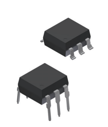
• DIP-6 package
• Clean bounce free switching
1
2
• TTL / CMOS compatible input
3
• Available on tape and reel
• Material categorization: for definitions of compliance
please see www.vishay.com/doc?99912
APPLICATIONS
DESCRIPTION
• Instrumentation
The VO14642 is a high speed single channel normally open
solid-state relay (SPST - 1 form A) in a DIP-6 package. The
relay is constructed as a multi-chip hybrid device. A high
efficient infrared LED enables low forward current on the
input side. On the output side high performance MOSFET
switches provide a low RON and can be configured for
AC/DC or DC only operation.
• Industrial controls
• Security
• Automatic measurement equipment
AGENCY APPROVALS
• UL1577
• cUL - UL1577
• DIN EN 60747-5-5 (VDE 0884-5) capable, consult sales
representative for details
Note
• Agency approvals are valid only for ambient temperature range
-40 °C to 85 °C
ORDERING INFORMATION
DIP-6
V
O
1
4
PART NUMBER
6
4
2
A
x
x
ELECTR.
PACKAGE
VARIATION CONFIG.
T
SMD-6
R
TAPE AND
REEL
PACKAGE
SMD-6, tape and reel
DIP-6, Tubes
Rev. 1.6, 12-Jun-17
VO14642AABTR
VO14642AT
Document Number: 81646
1
For technical questions, contact: optocoupleranswers@vishay.com
THIS DOCUMENT IS SUBJECT TO CHANGE WITHOUT NOTICE. THE PRODUCTS DESCRIBED HEREIN AND THIS DOCUMENT
ARE SUBJECT TO SPECIFIC DISCLAIMERS, SET FORTH AT www.vishay.com/doc?91000
�VO14642AT, VO14642AABTR
www.vishay.com
Vishay Semiconductors
ABSOLUTE MAXIMUM RATINGS (Tamb = 25 °C, unless otherwise specified)
PARAMETER
TEST CONDITION
SYMBOL
VALUE
UNIT
LED continous forward current
IF
50
mA
LED reverse voltage
VR
5
V
Pdiss
80
mW
DC or peak AC load voltage
VL
60
V
Load current (DC only)
IL
2
A
INPUT
LED power dissipation
At 25 °C
OUTPUT
Peak load current (AC/DC)
t = 10 ms
ILPK
3.6
A
Output power dissipation
At 25 °C
Pdiss
250
mW
mW
SSR
Total power dissipation
Pdiss
330
Ambient temperature range
Tamb
-55 to +85
°C
Storage temperature range
Tstg
-55 to +125
°C
Tsld
260
°C
t ≤ 10 s max.
Soldering temperature (1)
Notes
• Stresses in excess of the absolute maximum ratings can cause permanent damage to the device. Functional operation of the device is not
implied at these or any other conditions in excess of those given in the operational sections of this document. Exposure to absolute
maximum ratings for extended periods of the time can adversely affect reliability
(1) Refer to reflow profile for soldering conditions for surface mounted devices (SMD). Refer to wave profile for soldering conditions for through
hole devices (DIP)
ABSOLUTE MAXIMUM RATING CURVE
2.5
DC mode
Load Current/A
2.0
1.5
AC/DC mode
1.0
0.5
0.0
-50
-25
0
25
50
75
100
Ambient Temperature/°C
Fig. 1 - Load Current (AC/DC) vs. Temperature
THERMAL CHARACTERISTICS
PARAMETER
TEST CONDITION
SYMBOL
VALUE
UNIT
°C
Maximum LED junction temperature
At 25 °C
Tjmax.
125
Maximum output die junction temperature
At 25 °C
Tjmax.
125
°C
Thermal resistance, junction emitter to board
At 25 °C
θEB
176
°C/W
°C/W
Thermal resistance, junction emitter to case
At 25 °C
θEC
208
Thermal resistance, junction detector to board
At 25 °C
θDB
67
°C/W
Thermal resistance, junction detector to case
At 25 °C
θDC
134
°C/W
Thermal resistance, junction emitter to junction detector
At 25 °C
θED
310
°C/W
Thermal resistance, case to ambient
At 25 °C
θCA
2180
°C/W
Note
• The thermal model is represented in the thermal network below. Each resistance value given in this model can be used to calculate the
temperatures at each node for a given operating condition. The thermal resistance from board to ambient will be dependent on the type of
PCB, layout and thickness of copper traces. For a detailed explanation of the thermal model, please reference Vishay's thermal
characteristics of optocouplers application note
Rev. 1.6, 12-Jun-17
Document Number: 81646
2
For technical questions, contact: optocoupleranswers@vishay.com
THIS DOCUMENT IS SUBJECT TO CHANGE WITHOUT NOTICE. THE PRODUCTS DESCRIBED HEREIN AND THIS DOCUMENT
ARE SUBJECT TO SPECIFIC DISCLAIMERS, SET FORTH AT www.vishay.com/doc?91000
�VO14642AT, VO14642AABTR
www.vishay.com
Vishay Semiconductors
TA
θCA
Package
TC
θEC
θDC
θDE
TJD
TJE
θDB
θEB
TB
θBA
19996
TA
ELECTRICAL CHARACTERISTICS (Tamb = 25 °C, unless otherwise specified)
PARAMETER
TEST CONDITION
SYMBOL
MIN.
TYP.
MAX.
UNIT
INPUT
LED forward current, switch turn-on
IL = 1 A, VL ≤ 0.5 V, t = 10 ms
IFon
-
0.5
2
mA
LED forward current, switch turn-off
VL = 60 V, IL < 1 μA
IFoff
50
-
-
μA
LED reverse current
VR = 5 V
IR
-
-
10
μA
LED forward voltage
IF = 10 mA
VF
1
1.3
1.5
V
Ω
OUTPUT
On-resistance (AC/DC)
IF = 10 mA, IL = 1 A
RON
-
0.18
0.25
On-resistance (DC only)
IF = 10 mA, IL = 2 A
RON
-
0.05
0.07
Ω
Off-state leakage current
IF = 0 mA, VL = 60 V
ILEAK
-
-
1
μA
Note
• Minimum and maximum values are testing requirements. Typical values are characteristics of the device and are the result of engineering
evaluations. Typical values are for information only and are not part of the testing requirements
PIN CONFIGURATION
DC only configuration
AC/DC configuration
Anode
Cathode
Do not use
1
6
2
5
3
4
Load
Anode
Cathode
Load
Do not use
1
6
2
5
3
4
20545
SWITCHING CHARACTERISTICS (AC/DC CONNECTION)
PARAMETER
TEST CONDITION
SYMBOL
MIN.
TYP.
MAX.
UNIT
Turn-on time
IF = 10 mA, VL = 30 V, IL = 200 mA
ton
-
370
800
μs
Turn-off time
IF = 10 mA, VL = 30 V, IL = 200 mA
toff
-
50
800
μs
Turn-on time
IF = 10 mA, VL = 5 V, IL = 1 A
ton
-
550
-
μs
Turn-off time
IF = 10 mA, VL = 5 V, IL = 1 A
toff
-
18
-
μs
Rev. 1.6, 12-Jun-17
Document Number: 81646
3
For technical questions, contact: optocoupleranswers@vishay.com
THIS DOCUMENT IS SUBJECT TO CHANGE WITHOUT NOTICE. THE PRODUCTS DESCRIBED HEREIN AND THIS DOCUMENT
ARE SUBJECT TO SPECIFIC DISCLAIMERS, SET FORTH AT www.vishay.com/doc?91000
�VO14642AT, VO14642AABTR
www.vishay.com
Vishay Semiconductors
VL
1.25 ms
Input
Output
TON
TOFF
Output
90 %
10 %
20991-1
SAFETY AND INSULATION RATINGS
PARAMETER
TEST CONDITION
SYMBOL
Climatic classification
According to IEC 68 part 1
Pollution degree
According to DIN VDE 0109
Comparative tracking index
VALUE
UNIT
40 / 085 / 21
2
Insulation group IIIa
CTI
175
Maximum rated withstanding isolation voltage
According to UL1577, t = 1 min
VISO
5300
Maximum transient isolation voltage
According to DIN EN 60747-5-5
VIOTM
8000
Vpeak
Maximum repetitive peak isolation voltage
According to DIN EN 60747-5-5
VIORM
890
Vpeak
Tamb = 25 °C, VIO = 500 V
RIO
≥ 1012
Ω
Tamb = 100 °C, VIO = 500 V
RIO
≥ 1011
Ω
RIO
≥
Isolation resistance
Tamb = TS, VIO = 500 V
Output safety power
VRMS
Ω
109
PSO
400
mW
Input safety current
ISI
150
mA
Input safety temperature
TS
165
°C
≥7
mm
≥7
mm
≥ 0.4
mm
Creepage distance
Clearance distance
Insulation thickness
DTI
450
400
Output Power PSO
350
300
250
200
150
100
50
0
0
25
50
75
100 125 150 175 200
Ambient Temperature (°C)
Fig. 2 - Safety Derating (input)
Rev. 1.6, 12-Jun-17
Maximum Safety Input Current (mA)
Maximum Safety Output Power (mW)
Note
• This SSR is suitable for “safe electrical insulation” only within the safety ratings. Compliance with the safety ratings shall be ensured by
means of protective circuits
160
140
120
100
80
Input Current ISI
60
40
20
0
0
25
50
75
100 125 150 175 200
Ambient Temperature (°C)
Fig. 3 - Safety Derating (output)
Document Number: 81646
4
For technical questions, contact: optocoupleranswers@vishay.com
THIS DOCUMENT IS SUBJECT TO CHANGE WITHOUT NOTICE. THE PRODUCTS DESCRIBED HEREIN AND THIS DOCUMENT
ARE SUBJECT TO SPECIFIC DISCLAIMERS, SET FORTH AT www.vishay.com/doc?91000
�VO14642AT, VO14642AABTR
www.vishay.com
Vishay Semiconductors
TYPICAL CHARACTERISTICS (Tamb = 25 °C, unless otherwise specified)
1.7
IF = 50 mA
1.6
1.6
Tamb = -55 °C
1.5
LED Voltage (V)
VF - Forward Voltage (V)
1.8
1.4
1.2
1.0
Tamb = 25 °C
0.8
Tamb = +85 °C
IF = 30 mA
1.4
1.3
IF = 10 mA
1.2
IF = 5 mA
1.1
IF = 1 mA
0.6
1
10
1.0
100
-55
-35
IF - Forward Current (mA)
VR = 11V
LED Leakage Current (nA)
1.20
1.00
0.80
0.60
0.40
0.20
0.00
-35
-15
5
25
45
65
60
40
20
0
-20
-40
-55
-35
-15
Leakage Current (nA)
30
25
20
15
10
5
0
5
25
45
65
Temperature (°C)
Fig. 6 - Leakage Current vs. Temperature
Rev. 1.6, 12-Jun-17
5
25
45
65
85
85
Fig. 8 - LED Forward Current for Switch Turn-On vs. Temperature
ON-Resistance, Normalized to 25°C
VLoad = 60 V
-15
85
Temperature (°C)
40
-35
65
80
85
Fig. 5 - LED Leakage Current vs. Ambient Temperature
-55
45
100
Tamb - Ambient Temperature (°C)
35
25
Fig. 7 - LED Voltage vs. Temperature
LED Forward Current for Switch
Turn-on normalized to 25 °C (%)
1.60
-55
5
Temperature (°C)
Fig. 4 - Forward Voltage vs. Forward Current
1.40
-15
1.8
IF = 10 mA
IL = 1 A
1.6
1.4
1.2
1.0
0.8
0.6
0.4
-55
-35
-15
5
25
45
65
85
Temperature (°C)
Fig. 9 - On-Resistance vs. Temperature
Document Number: 81646
5
For technical questions, contact: optocoupleranswers@vishay.com
THIS DOCUMENT IS SUBJECT TO CHANGE WITHOUT NOTICE. THE PRODUCTS DESCRIBED HEREIN AND THIS DOCUMENT
ARE SUBJECT TO SPECIFIC DISCLAIMERS, SET FORTH AT www.vishay.com/doc?91000
�VO14642AT, VO14642AABTR
www.vishay.com
Vishay Semiconductors
2200
25
IL = 1 A, tP = 5 ms
IF = 10 mA, IL = 1 A, tP = 5 ms
20
Turn-on Time (μs)
Turn-off Time (μs)
1800
15
10
1400
1000
T = 25 °C
T = 85 °C
600
T = -55 °C
200
5
-55
-35
-15
5
25
45
65
5
85
Temperature ( C)
Fig. 10 - Turn-Off Time vs. Temperature
15
20
Fig. 13 - Turn-On Time vs. Forward Current
250
30
Switch Capacitance (pF)
IL = 1 A, tP = 5 ms
25
Turn-off Time (μs)
10
IF - Forward Current (mA)
T = 85°C
20
15
T = 25°C
10
T = -55°C
5
T = 25°C
200
150
100
50
0
0
5
10
15
20
Forward Current (mA)
0
20
40
60
Applied Voltage (V)
Fig. 11 - Turn-Off Time vs. Forward Current
Fig. 14 - Switch Capacitance vs. Applied Voltage
1000
IF = 10 mA, IL = 1A, tP = 5 ms
Turn-on Time (μs)
900
800
700
600
500
-55
-35
-15
5
25
45
65
85
Temperature (°C)
Fig. 12 - Turn-On Time vs. Temperature
Rev. 1.6, 12-Jun-17
Document Number: 81646
6
For technical questions, contact: optocoupleranswers@vishay.com
THIS DOCUMENT IS SUBJECT TO CHANGE WITHOUT NOTICE. THE PRODUCTS DESCRIBED HEREIN AND THIS DOCUMENT
ARE SUBJECT TO SPECIFIC DISCLAIMERS, SET FORTH AT www.vishay.com/doc?91000
�VO14642AT, VO14642AABTR
www.vishay.com
Vishay Semiconductors
PACKAGE DIMENSIONS (in millimeters)
SMD-6
9.80 ± 0.25
7.62 typ.
7.25 ± 0.10
6.65 ± 0.15
0.25 ± 0.20
1.00 ± 0.10
2.54 nom.
2 x 2.54 = 5.08
6
5
0.25 ± 0.10
3.55 ± 0.25
0.79 typ.
7.60 max.
0.60 min.
Leads coplanarity
0.1 max.
8.00 min.
4
2.54
1.50
5.08
Recommended footprint
Pin one I.D.
8.0 min.
1.50
11.00
1
2
3
DIP-6
7.60 max.
7.25 ± 0.10
7.62 typ.
6.65 ± 0.15
6.09 ± 0.25
1.00 ± 0.10
3.04 ± 0.25
0.70 ± 0.20
3.55 ± 0.25
0.79 typ.
0.50 ± 0.10
3° to 9
2.54 nom.
2 x 2.54 = 5.08
6
5
4
1
2
3
°
.10
0.25 ± 0
Pin one I.D.
Rev. 1.6, 12-Jun-17
Document Number: 81646
7
For technical questions, contact: optocoupleranswers@vishay.com
THIS DOCUMENT IS SUBJECT TO CHANGE WITHOUT NOTICE. THE PRODUCTS DESCRIBED HEREIN AND THIS DOCUMENT
ARE SUBJECT TO SPECIFIC DISCLAIMERS, SET FORTH AT www.vishay.com/doc?91000
�VO14642AT, VO14642AABTR
www.vishay.com
Vishay Semiconductors
PACKAGE MARKING
VO14642
V YWW 68
Note
• Tape and reel suffix “TR” is not part of the package marking
PACKING INFORMATION (in millimeters)
2.0 ± 0.1
0.35 ± 0.05
4.0 ± 0.1
1.75 ± 0.1
1.5 min.
Pin 1
7.5 ± 0.1
16.0 ± 0.3
CL
7.77 ± 0.1
3.9 ± 0.1
4.4 ± 0.1
12.0 ± 0.1
10.3 ± 0.1
1.5 min.
Fig. 15 - Tape and Reel Packing
TAPE AND REEL PACKING
TYPE
UNITS/REEL
SMD-6
1000
TUBE PACKING
TYPE
UNITS/TUBE
TUBES/BOX
UNITS/BOX
DIP-6
50
40
2000
SOLDER PROFILES
300
300
5s
Lead temperature
ca. 2 K/s
2 K/s
50
full line: typical
dotted line:
process limits
second
wave
Temperature (°C)
Temperature (°C)
235 °C to
260 °C
first wave
200
wave
ca. 200 K/s
150
100 °C to
130 °C
100
200
max. 30 s
150
max. ramp down 6 °C/s
50
0
94 8626
50
100
max. 100 s
max. 120 s
100
ca. 5 K/s
forced cooling
0
max. 260 °C
245 °C
255 °C
240 °C
217 °C
250
250
max. ramp up 3 °C/s
0
150
200
250
Time (s)
Fig. 16 - Wave Soldering Double Wave Profile According to
J-STD-020 for DIP Devices
0
19841
50
100
150
200
250
300
Time (s)
Fig. 17 - Lead (Pb)-free Reflow Solder Profile According to
J-STD-020 for SMD Devices
HANDLING AND STORAGE CONDITIONS
ESD level: HBM class 2
Floor life: unlimited
Conditions: Tamb < 30 °C, RH < 85 %
Moisture sensitivity level 1, according to J-STD-020
Rev. 1.6, 12-Jun-17
Document Number: 81646
8
For technical questions, contact: optocoupleranswers@vishay.com
THIS DOCUMENT IS SUBJECT TO CHANGE WITHOUT NOTICE. THE PRODUCTS DESCRIBED HEREIN AND THIS DOCUMENT
ARE SUBJECT TO SPECIFIC DISCLAIMERS, SET FORTH AT www.vishay.com/doc?91000
�Footprint and Schematic Information
www.vishay.com
Vishay Semiconductors
Footprint and Schematic Information for
VO14642AAB, VO14642AT
The footprint and schematic symbols for the following parts can be accessed using the associated links. They are available in
Eagle, Altium, KiCad, OrCAD / Allegro, Pulsonix, and PADS.
Note that the 3D models for these parts can be found on the Vishay product page.
PART NUMBER
VO14642AAB
VO14642AT
FOOTPRINT / SCHEMATIC
www.snapeda.com/parts/VO14642AAB/Vishay/view-part
www.snapeda.com/parts/VO14642AT/Vishay/view-part
For technical issues and product support, please contact optocoupleranswers@vishay.com.
Rev. 1.0, 15-May-17
Document Number: 84539
1
For technical questions, contact: optocoupleranswers@vishay.com
THIS DOCUMENT IS SUBJECT TO CHANGE WITHOUT NOTICE. THE PRODUCTS DESCRIBED HEREIN AND THIS DOCUMENT
ARE SUBJECT TO SPECIFIC DISCLAIMERS, SET FORTH AT www.vishay.com/doc?91000
�Legal Disclaimer Notice
www.vishay.com
Vishay
Disclaimer
ALL PRODUCT, PRODUCT SPECIFICATIONS AND DATA ARE SUBJECT TO CHANGE WITHOUT NOTICE TO IMPROVE
RELIABILITY, FUNCTION OR DESIGN OR OTHERWISE.
Vishay Intertechnology, Inc., its affiliates, agents, and employees, and all persons acting on its or their behalf (collectively,
“Vishay”), disclaim any and all liability for any errors, inaccuracies or incompleteness contained in any datasheet or in any other
disclosure relating to any product.
Vishay makes no warranty, representation or guarantee regarding the suitability of the products for any particular purpose or
the continuing production of any product. To the maximum extent permitted by applicable law, Vishay disclaims (i) any and all
liability arising out of the application or use of any product, (ii) any and all liability, including without limitation special,
consequential or incidental damages, and (iii) any and all implied warranties, including warranties of fitness for particular
purpose, non-infringement and merchantability.
Statements regarding the suitability of products for certain types of applications are based on Vishay’s knowledge of
typical requirements that are often placed on Vishay products in generic applications. Such statements are not binding
statements about the suitability of products for a particular application. It is the customer’s responsibility to validate that a
particular product with the properties described in the product specification is suitable for use in a particular application.
Parameters provided in datasheets and / or specifications may vary in different applications and performance may vary over
time. All operating parameters, including typical parameters, must be validated for each customer application by the customer’s
technical experts. Product specifications do not expand or otherwise modify Vishay’s terms and conditions of purchase,
including but not limited to the warranty expressed therein.
Except as expressly indicated in writing, Vishay products are not designed for use in medical, life-saving, or life-sustaining
applications or for any other application in which the failure of the Vishay product could result in personal injury or death.
Customers using or selling Vishay products not expressly indicated for use in such applications do so at their own risk.
Please contact authorized Vishay personnel to obtain written terms and conditions regarding products designed for
such applications.
No license, express or implied, by estoppel or otherwise, to any intellectual property rights is granted by this document
or by any conduct of Vishay. Product names and markings noted herein may be trademarks of their respective owners.
© 2019 VISHAY INTERTECHNOLOGY, INC. ALL RIGHTS RESERVED
Revision: 01-Jan-2019
1
Document Number: 91000
�


 工商网监
湘ICP备2023018690号
工商网监
湘ICP备2023018690号