TB62215AFG
BiCD Integrated Circuit
Silicon Monolithic
TB62215AFG
PWM Method Clock In Bipolar Stepping Motor Driver IC
The TB62215AFG is a two-phase bipolar stepping motor driver using a PWM chopper.
Fabricated with the BiCD process, the TB62215AFG is rated at 40 V/3.0 A .
The on-chip voltage regulator allows control of a stepping motor with a single VM power
supply.
Features
Bipolar stepping motor driver
PWM constant-current drive
Clock input control
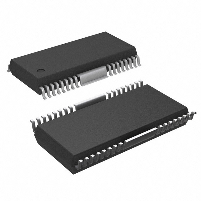
HSOP28-P-0450-0.80
Allows two-phase, 1-2-phase and W1-2-phase excitations.
Weight 0.79g(typ.)
BiCD process: Uses DMOS FETs as output power transistors.
High voltage and current: 40 V/3.0 A (absolute maximum ratings)
Thermal shutdown (TSD), overcurrent shutdown (ISD), and power-on-resets (PORs)
Do not design your products or systems based on the information on this document.
Please contact your Toshiba sales representative for updated information before designing your
products.
1
2012-6-4
�TB62215AFG
Block Diagram
Oscillator
VREF Comparator
Logic
TSD/ISD/VRS Detect
VREG
Ach
Pre-driver
Bch
Pre-driver
Functional blocks/circuits/constants in the block chart etc. may be omitted or simplified for explanatory
purposes.
2
2012-6-4
�TB62215AFG
Pin Assignment
(Top View)
CW/CCW
1
28
OSCM
MO_OUT
2
27
VREF_A
D_MODE1
3
26
VREF_B
D_MODE2
4
25
NC
CLK_IN
5
24
NC
ENABLE
6
23
VCC
RESET
7
22
VM
FIN
TB62215AFG
FIN
RS_A
8
21
RS_B
NC
9
20
NC
OUT_B
NC
10
11
19
18
NC
PGND
12
17
PGND
OUT_A-
13
16
OUT_B-
PGND
14
15
PGND
OUT_A
3
2012-6-4
�TB62215AFG
Pin Function
Pin number
Pin name
Function
1
CW/CCW
Normal rotation/reversal of motor operation
2
MO_OUT
Electric corner monitor terminal
3
D_MODE1
Excitation setting terminal 1
4
D_MODE2
5
CLK_IN
6
ENABLE
Excitation setting terminal 2
Clock input terminal that decides rotational speed of motor. An electric corner advances
by standing up.
Output ON (5V)/turning off (GND) switch terminal of A and B channel.
7
RESET
8
RS_A
9
NC
10
OUT_A
11
NC
12
PGND
13
OUT_A-
14
PGND
Power GND for motor drive
15
PGND
Power GND for motor drive
16
OUT_B-
17
PGND
18
NC
19
OUT_B
20
NC
21
RS_B
22
VM
23
VCC
Monitor terminal for internal generation 5V
24
NC
No connection
25
NC
No connection
26
VREF_B
27
VREF_A
28
OSCM
An electric corner is initialized.
Sense resistance connection terminal for current value setting of A channel output
(Power supply terminal)
No connection
A channel output plus terminal
No connection
Power GND for motor drive
A channel output minus terminal
B channel output minus terminal
Power GND for motor drive
No connection
B channel output plus terminal
No connection
Sense resistance connection terminal for current value setting of B channel output
(Power supply terminal)
Motor power supply monitor terminal
Bias terminal for current value setting of B channel output
Bias terminal for current value setting of A channel output
Setting of frequency of oscillation circuit terminal for chopper
4
2012-6-4
�TB62215AFG
Function
1. CLK
CLK Input
Function
Rise
The electrical angle leads by one on the rising edge.
Fall
Remains at the same position.
2. ENABLE
ENABLE Input
Function
H
Output transistors are enabled (normal operation mode).
L
Output transistors are disabled (high impedance state).
3. CW/CCW
CW/CCW Input
Function
OUT (+)
OUT (-)
H
Forward (CW)
H
L
L
Reverse (CCW)
L
H
X: Don't care
4. DMODE
D_MODE1
D_MODE2
L
L
OSC_M, output transistors are disabled (in Standby mode)
L
H
Two-phase excitation
H
L
1-2-phase excitation
H
H
W1-2-phase excitation
Function
5. RESET
RESET Input
Function
L
Normal operation mode
H
The electrical angle is reset.
5
2012-6-4
�TB62215AFG
Absolute Maximum Ratings (Ta = 25°C)
Characteristics
Symbol
Rating
Unit
Motor power supply
VM
40
V
Motor output voltage
VOUT
40
V
Motor output current
IOUT_S
3.0
A
Logic power supply
VCC
6
V
Digital input voltage
VIN
6
V
MO output voltage
VMO
6
V
MO output sink current
IMO
30.0
mA
Power dissipation
PD
1.3
W
Operating temperature
Topr
-20 to 85
°C
Storage temperature
Tstg
-55 to 150
°C
Junction temperature
Tj(Max)
150
°C
Operation Ranges
Characteristics
Symbol
Test Condition
Min
Typ.
Max
Unit
Motor power supply
VM
-
10
24
38
V
Motor output current
IOUT
Ta=25°C,1corresponding worth
-
1.8
2.4
A
VIN(H)
H level of logic
2.0
-
5.5
V
VIN(L)
L level of logic
-0.4
-
1.0
V
MO output voltage
VMO
With a pull-up resistor
-
3.3
5.5
V
Clock input frequency
fCLK
-
-
-
100
kHz
Chopper frequency
fchop
-
40
100
150
kHz
Vref reference voltage
Vref
-
GND
-
3.6
V
Voltage across the current-sensing resistor pins
VRS
-
0.0
±1.0
±1.5
V
Digital input voltage
This document is for reference only. Please contact us for sample datasheets.
6
2012-6-4
�TB62215AFG
Electrical Characteristics (Ta = 25°C, VM = 24 V, unless otherwise specified)
Characteristics
Digital input voltage
Symbol
VIH
Test Condition
Digital input pins
VIL
Min
Typ.
Max
2.0
3.3
5.5
GND
-
0.8
Unit
V
Supply current
IM
Outputs open (two-phase excitation)
-
5
7
mA
Channel-to-channel differential
ΔIOUT1
IOUT = 2.0A
-5
0
5
%
Output current error relative to
the predetermined value
ΔIOUT2
IOUT = 2.0A
-5
0
5
%
Drain-source
ON-resistance of the output
transistors
(upper and lower sum)
RON(D-S)
IOUT = 2.0A,Tj = 25°C
0.4
0.6
0.8
Ω
Power-supply voltage for
internal circuit operation
VCC
ICC=5.0mA
4.75
5.00
5.25
V
Power-supply current for
internal circuit operation
ICC
-
-
2.5
5.0
mA
VM recovery voltage
VMR
-
7.0
8.0
9.0
V
Overcurrent trip threshold
ISD
-
3.0
4.0
5.0
A
7
2012-6-4
�TB62215AFG
Package Dimensions
8
2012-6-4
�TB62215AFG
Notes on Contents
Block Diagrams
Functional blocks/circuits/constants in the block chart etc. may be omitted or simplified for explanatory
purposes.
IC Usage Considerations
Notes on handling of ICs
The absolute maximum ratings of a semiconductor device are a set of ratings that must not be exceeded, even for a
moment. Do not exceed any of these ratings.
Exceeding the rating(s) may cause device breakdown, damage or deterioration, and may result in injury by
explosion or combustion.
Use an appropriate power supply fuse to ensure that a large current does not continuously flow in the case of
overcurrent and/or IC failure. The IC will fully break down when used under conditions that exceed its absolute
maximum ratings, when the wiring is routed improperly or when an abnormal pulse noise occurs from the wiring
or load, causing a large current to continuously flow and the breakdown can lead to smoke or ignition. To minimize
the effects of the flow of a large current in the case of breakdown, appropriate settings, such as fuse capacity, fusing
time and insertion circuit location, are required.
If your design includes an inductive load such as a motor coil, incorporate a protection circuit into the design to
prevent device malfunction or breakdown caused by the current resulting from the inrush current at power ON or
the negative current resulting from the back electromotive force at power OFF. IC breakdown may cause injury,
smoke or ignition.
Use a stable power supply with ICs with built-in protection functions. If the power supply is unstable, the
protection function may not operate, causing IC breakdown. IC breakdown may cause injury, smoke or ignition.
Do not insert devices in the wrong orientation or incorrectly.
Make sure that the positive and negative terminals of power supplies are connected properly.
Otherwise, the current or power consumption may exceed the absolute maximum rating, and exceeding the
rating(s) may cause device breakdown, damage or deterioration, and may result in injury by explosion or
combustion.
In addition, do not use any device inserted in the wrong orientation or incorrectly to which current is applied even
just once.
Carefully select external components (such as inputs and negative feedback capacitors) and load components (such
as speakers), for example, power amp and regulator.
If there is a large amount of leakage current such as from input or negative feedback condenser, the IC output DC
voltage will increase. If this output voltage is connected to a speaker with low input withstand voltage, overcurrent
or IC failure may cause smoke or ignition. (The overcurrent may cause smoke or ignition from the IC itself.) In
particular, please pay attention when using a Bridge Tied Load (BTL) connection-type IC that inputs output DC
voltage to a speaker directly.
9
2012-6-4
�TB62215AFG
Points to remember when handling of ICs
Overcurrent Protection Circuit
Overcurrent protection circuits (referred to as current limiter circuits) do not necessarily protect ICs under all
circumstances. If the overcurrent protection circuits operate against the overcurrent, clear the overcurrent status
immediately.
Depending on the method of use and usage conditions, exceeding absolute maximum ratings may cause the
overcurrent protection circuit to operate improperly or IC breakdown may occur before operation. In addition,
depending on the method of use and usage conditions, if overcurrent continues to flow for a long time after
operation, the IC may generate heat resulting in breakdown.
Thermal Shutdown Circuit
Thermal shutdown circuits do not necessarily protect ICs under all circumstances. If the thermal shutdown circuits
operate against the over-temperature, clear the heat generation status immediately.
Depending on the method of use and usage conditions, exceeding absolute maximum ratings may cause the thermal
shutdown circuit to operate improperly or IC breakdown to occur before operation.
Heat Radiation Design
When using an IC with large current flow such as power amp, regulator or driver, design the device so that heat is
appropriately radiated, in order not to exceed the specified junction temperature (TJ) at any time or under any
condition. These ICs generate heat even during normal use. An inadequate IC heat radiation design can lead to
decrease in IC life, deterioration of IC characteristics or IC breakdown. In addition, when designing the device, take
into consideration the effect of IC heat radiation with peripheral components.
Back-EMF
When a motor rotates in the reverse direction, stops or slows abruptly, current flows back to the motor’s power
supply owing to the effect of back-EMF. If the current sink capability of the power supply is small, the device’s
motor power supply and output pins might be exposed to conditions beyond the absolute maximum ratings. To
avoid this problem, take the effect of back-EMF into consideration in system design.
10
2012-6-4
�TB62215AFG
RESTRICTIONS ON PRODUCT USE
Toshiba Corporation, and its subsidiaries and affiliates (collectively "TOSHIBA"), reserve the right to make changes to the information
in this document, and related hardware, software and systems (collectively "Product") without notice.
This document and any information herein may not be reproduced without prior written permission from TOSHIBA. Even with
TOSHIBA's written permission, reproduction is permissible only if reproduction is without alteration/omission.
Though TOSHIBA works continually to improve Product's quality and reliability, Product can malfunction or fail. Customers are
responsible for complying with safety standards and for providing adequate designs and safeguards for their hardware, software and
systems which minimize risk and avoid situations in which a malfunction or failure of Product could cause loss of human life, bodily
injury or damage to property, including data loss or corruption. Before customers use the Product, create designs including the
Product, or incorporate the Product into their own applications, customers must also refer to and comply with (a) the latest versions of
all relevant TOSHIBA information, including without limitation, this document, the specifications, the data sheets and application notes
for Product and the precautions and conditions set forth in the "TOSHIBA Semiconductor Reliability Handbook" and (b) the
instructions for the application with which the Product will be used with or for. Customers are solely responsible for all aspects of their
own product design or applications, including but not limited to (a) determining the appropriateness of the use of this Product in such
design or applications; (b) evaluating and determining the applicability of any information contained in this document, or in charts,
diagrams, programs, algorithms, sample application circuits, or any other referenced documents; and (c) validating all operating
parameters for such designs and applications. TOSHIBA ASSUMES NO LIABILITY FOR CUSTOMERS' PRODUCT DESIGN OR
APPLICATIONS.
PRODUCT IS NEITHER INTENDED NOR WARRANTED FOR USE IN EQUIPMENTS OR SYSTEMS THAT REQUIRE
EXTRAORDINARILY HIGH LEVELS OF QUALITY AND/OR RELIABILITY, AND/OR A MALFUNCTION OR FAILURE OF WHICH
MAY CAUSE LOSS OF HUMAN LIFE, BODILY INJURY, SERIOUS PROPERTY DAMAGE AND/OR SERIOUS PUBLIC IMPACT
("UNINTENDED USE"). Except for specific applications as expressly stated in this document, Unintended Use includes, without
limitation, equipment used in nuclear facilities, equipment used in the aerospace industry, medical equipment, equipment used for
automobiles, trains, ships and other transportation, traffic signaling equipment, equipment used to control combustions or explosions,
safety devices, elevators and escalators, devices related to electric power, and equipment used in finance-related fields. IF YOU USE
PRODUCT FOR UNINTENDED USE, TOSHIBA ASSUMES NO LIABILITY FOR PRODUCT. For details, please contact your
TOSHIBA sales representative.
Do not disassemble, analyze, reverse-engineer, alter, modify, translate or copy Product, whether in whole or in part.
Product shall not be used for or incorporated into any products or systems whose manufacture, use, or sale is prohibited under any
applicable laws or regulations.
The information contained herein is presented only as guidance for Product use. No responsibility is assumed by TOSHIBA for any
infringement of patents or any other intellectual property rights of third parties that may result from the use of Product. No license to
any intellectual property right is granted by this document, whether express or implied, by estoppel or otherwise.
ABSENT A WRITTEN SIGNED AGREEMENT, EXCEPT AS PROVIDED IN THE RELEVANT TERMS AND CONDITIONS OF SALE
FOR PRODUCT, AND TO THE MAXIMUM EXTENT ALLOWABLE BY LAW, TOSHIBA (1) ASSUMES NO LIABILITY
WHATSOEVER, INCLUDING WITHOUT LIMITATION, INDIRECT, CONSEQUENTIAL, SPECIAL, OR INCIDENTAL DAMAGES OR
LOSS, INCLUDING WITHOUT LIMITATION, LOSS OF PROFITS, LOSS OF OPPORTUNITIES, BUSINESS INTERRUPTION AND
LOSS OF DATA, AND (2) DISCLAIMS ANY AND ALL EXPRESS OR IMPLIED WARRANTIES AND CONDITIONS RELATED TO
SALE, USE OF PRODUCT, OR INFORMATION, INCLUDING WARRANTIES OR CONDITIONS OF MERCHANTABILITY, FITNESS
FOR A PARTICULAR PURPOSE, ACCURACY OF INFORMATION, OR NONINFRINGEMENT.
Do not use or otherwise make available Product or related software or technology for any military purposes, including without
limitation, for the design, development, use, stockpiling or manufacturing of nuclear, chemical, or biological weapons or missile
technology products (mass destruction weapons). Product and related software and technology may be controlled under the
applicable export laws and regulations including, without limitation, the Japanese Foreign Exchange and Foreign Trade Law and the
U.S. Export Administration Regulations. Export and re-export of Product or related software or technology are strictly prohibited
except in compliance with all applicable export laws and regulations.
Please contact your TOSHIBA sales representative for details as to environmental matters such as the RoHS compatibility of Product.
Please use Product in compliance with all applicable laws and regulations that regulate the inclusion or use of controlled substances,
including without limitation, the EU RoHS Directive. TOSHIBA ASSUMES NO LIABILITY FOR DAMAGES OR LOSSES
OCCURRING AS A RESULT OF NONCOMPLIANCE WITH APPLICABLE LAWS AND REGULATIONS.
11
2012-6-4
�


 工商网监
湘ICP备2023018690号
工商网监
湘ICP备2023018690号
