TLP2631
TOSHIBA photocoupler
GaAℓAs IRed & Photo IC
TLP2631
Isolated Line Receiver
Simplex / Multiplex Data Transmission
Computer-Peripheral Interface
Microprocessor System Interface
Digital Isolation for A / D, D / A Conversion
Unit: mm
The TOSHIBA TLP2631 dual photocoupler consists of a pair of GaAℓAs
light emitting diode and integrated high gain, high speed photodetector.
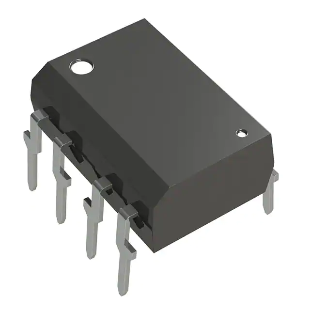
This unit is 8-lead DIP.
The output of the detector circuit is an open collector, Schottky clamped
transistor.
A Faraday shield integrated on the photodetector chip reduces the effects
of capacitive coupling between the input LED emitter and the high gain
stages of the detector. This provides an effective common mode transient
immunity of 1000 V/μs.
• Input current threshold: IF = 5 mA (max)
•
Switching speed: 10MBd (typ.)
•
Common mode transient immunity: ±1000 V/μs (min)
•
Guaranteed performance over temperature: 0 to 70°C
•
Isolation voltage: 2500 Vrms (min)
•
UL recognized: UL1577, file no. E67349
•
cUL approved :CSA Component Acceptance Service
No. 5A, File No.E67349
TOSHIBA
11−10C4
Weight: 0.54 g (typ.)
Truth Table (positive logic)
Input
Output
H
L
Pin Configuration (top view)
1
L
+
VF1
−
+
VF2
−
IF1
ICC
8
7
2
IF2
2
7
3
6
4
Shield
IO1
4
8
H
Schematic
1
VCC
IO2
6
VCC
GND
Shield
5
1 : Anode 1
2 : Cathode 1
3 : Cathode 2
4 : Anode 2
5 : GND
6 : VO2 (Output 2)
7 : VO1 (Output 1)
8 : VCC
VO1
VO2
3
5
GND
A 0.01 to 0.1μF bypass capacitor must be
connected between pins 8 and 5(see Note 1).
Start of commercial production
1986-03
1
2017-08-21
�TLP2631
Absolute Maximum Ratings (no derating required up to 70°C)
Symbol
Rating
Unit
Forward current (each channel)
IF
20
mA
Pulse forward current (each channel)*
IFP
30
mA
Reverse voltage (each channel)
VR
5
V
Input power dissipation(each channel)
PD
25
mW
ΔPD/°C
-0.45
mW/°C
Output current (each channel)
IO
16
mA
Output voltage (each channel)
VO
−0.5 to 7
V
VCC
7
V
PO
40
mW
ΔPO/°C
-0.75
mW/°C
Storage temperature range
Tstg
−55 to 125
°C
Operating temperature range
Topr
−40 to 85
°C
Lead soldering temperature (10s)**
Tsol
260
°C
BVS
2500
Vrms
LED
Characteristic
Input power dissipation
(each channel)
(Ta ≥ 70°C)
derating
Detector
Supply voltage
(1 minute maximum)
Output collector power
dissipation (each channel)
Output power dissipation
(each channel)
derating
(Ta ≥ 70°C)
Isolation voltage
(AC, 1 minute, R.H.≤ 60%, Ta=25°C
(Note 3)
Note: Using continuously under heavy loads (e.g. the application of high temperature/current/voltage and the
significant change in temperature, etc.) may cause this product to decrease in the reliability significantly even if
the operating conditions (i.e. operating temperature/current/voltage, etc.) are within the absolute maximum
ratings and the operating ranges.
Please design the appropriate reliability upon reviewing the Toshiba Semiconductor Reliability Handbook
(“Handling Precautions”/“Derating Concept and Methods”) and individual reliability data (i.e. reliability test
report and estimated failure rate, etc).
* t ≤ 1 msec duration.
** 2mm below seating plane.
Recommended Operating Conditions
Characteristic
Symbol
Min
Typ.
Max
Unit
Input current, low level, each channel
IFL
0
―
250
μA
Input current, high level, each channel
IFH
6.3*
―
20
mA
Supply voltage**
VCC
4.5
5
5.5
V
N
―
―
8
Topr
0
―
70
Fan out (TTL load, each channel)
Operating temperature
°C
Note: Recommended operating conditions are given as a design guideline to obtain expected performance of the
device. Additionally, each item is an independent guideline respectively. In developing designs using this
product, please confirm specified characteristics shown in this document.
*
6.3mA is a guard banded value which allows for at least 20% CTR degradation.
Initial input current threshold value is 5.0 mA or less.
** This item denotes operating ranges, not meaning of recommended operating conditions.
2
2017-08-21
�TLP2631
Electrical Characteristics (Ta = 0 to 70°C unless otherwise noted)
Characteristic
Input forward voltage
(each channel)
Symbol
VF
Input diode temperature
coefficient (each channel)
ΔVF / ΔTa
Input reverse breakdown
voltage (each channel)
BVR
Test Condition
Min
Typ. *
Max
Unit
IF = 10mA, Ta = 25°C
―
1.65
1.75
V
IF = 10mA
―
−2.0
―
mV / °C
IR = 10μA, Ta = 25°C
5
―
―
V
Input capacitance
(each channel)
CT
VF = 0V, f = 1MHz
―
45
―
pF
High level output current
(each channel)
IOH
VCC = 5.5V, VO = 5.5V
IF = 250μA
―
1
250
μA
Low level output voltage
(each channel)
VOL
VCC = 5.5V, IF = 5mA
IOL(sinking) = 13mA
―
0.4
0.6
V
High level supply current
(both channels)
ICCH
VCC = 5.5V, IF = 0 mA
―
14
30
mA
Low level supply current
(both channels)
ICCL
VCC = 5.5V, IF = 10mA
―
24
38
mA
Isolation voltage
RS
VS = 500V, R.H. ≤ 60%
(Note 3)
5×10¹⁰
1014
―
Ω
Capacitance (input−output)
CS
f = 1MHz
(Note 3)
―
0.6
―
pF
Input−input leakage current
II−I
R.H. ≤ 60%, t = 5s
VI−I = 500V
(Note 6)
―
0.005
―
μA
Resistance (input−input)
RI−I
VI−I = 500V
(Note 6)
―
1011
―
Ω
Capacitance (input−input)
CI−I
f = 1MHz
(Note 6)
―
0.25
―
pF
* All typical values are at VCC = 5V, Ta = 25°C.
3
2017-08-21
�TLP2631
Switching Characteristics (Ta = 25°C, VCC = 5V)
Symbol
Test
Circuit
Propagation delay time to
low output level
tpHL
1
Propagation delay time to
high output level
tpLH
Output rise time, output
fall time (10 to 90%)
tr, tf
Characteristic
Test Condition
Min
Typ.
Max
Unit
IF = 0→7.5mA, RL = 350Ω
CL = 15pF (each channel)
―
60
75
ns
1
IF = 7.5mA→0, RL = 350Ω
CL = 15pF (each channel)
―
60
75
ns
1
IF = 0 7.5mA, RL = 350Ω
CL = 15pF (each channel)
―
30
―
ns
1000
10000
―
V / μs
−1000
−10000
―
V / μs
Common mode transient
immunity at high output level
CMH
2
IF = 0 mA, RL = 350Ω
VCM = 400V,
VO(min.) = 2V
(each channel, Note 4)
Common mode transient
immunity at low output level
CML
2
IF = 7.5mA, RL = 350Ω
VCM = 400V
VO(max.) = 0.8V
(each channel, Note 5)
(Note 1) 2mm below seating plane
(Note 2) The VCC supply voltage to each TLP2631 isolator must be bypassed by a 0.1μF capacitor or larger. This
can be either a ceramic or solid tantalum capacitor with good high frequency characteristic and should be
connected as close as possible to the package VCC and GND pins each device.
(Note 3) Device considered a two−terminal device: Pins 1, 2, 3 and 4 shorted together, and pins 5, 6, 7 and 8
shorted together.
(Note 4) CMH・the maximum tolerable rate of rise of the common mode voltage to ensure the output will remain in
the high state (i.e. VOUT > 2.0V).
Measured in volts per microsecond (V / μs).
Volts/ microsecond can be translated to sinusoidal voltages:
V / μs =
(dVCM)
Max. = fCM VCM (p.p.)
dt
Example:
VCM = 319Vpp when fCM = 1MHz using CML and CMH = 1000V / μs data sheet specified minimum.
(Note 5) CML・the maximum tolerable rate of fall of the common mode voltage to ensure the output will remain in
the low output state (i.e. VOUT < 0.8V).
Measured in volts per microsecond (V / μs).
(Note 6) Measured between pins 1 and 2 shorted together, and pins 3 and 4 shorted together.
4
2017-08-21
�TLP2631
Test Circuit 1. tpHL and tpLH
5V
VCC
1
100Ω
IF Monitor
2
7
3
6
4
GND 5
7.5mA
3.75mA
0mA
IF
8
0.1μF
Pulse input
PW = 10μs
Duty cycle = 1/10
RL
350Ω
tr
tf
5V
VO Monitor
CL
4.5V
VO
tpHL
* CL is approximately 15pF which includes probe and stray
1.5V
0.5V
VOL
tpLH
wiring capacitance.
Test Circuit 2. Transient Immunity and Typical Waveforms
VCC
1
2
B
A
VFF
7
3
6
4
GND 5
VCM
+
5V
8
0.1μF
IF
CL
10%
tr
0V
tf
VO Monitor
VO
(IF = 0mA)
−
5V
2V
0.8V
VO
Pulse generator
VOL
(IF = 7.5mA)
ZO = 50Ω
CMH =
VCM
RL
350Ω
400V
90%
320(V)
320(V)
, CML =
t r (μs)
t r (μs)
* CL is approximately 15pF which includes probe and stray
wiring capacitance.
5
2017-08-21
�TLP2631
ΔVF / ΔTa – IF
IF – VF
−2.6
100
Forward voltage temperature
coefficient ΔVF / ΔTa (mV / °C)
Forward current IF (mA)
Ta = 25 °C
10
1
0.1
0.01
1.0
1.2
1.4
Forward voltage VF
−2.2
−2.0
−1.8
−1.6
−1.4
0.1
2.0
1.8
1.6
−2.4
1
0.3
(V)
3
Forward current IF
100
High level output current IOH (μA)
Output voltage VO
(V)
Ta = 25 °C
6
RL = 350Ω
1kΩ
4kΩ
2
1
2
50
IF = 250 μA
VCC = 5 V
0
0
30
IOH – Ta
V O – IF
8
4
10
(mA)
3
4
Forward current IF
5
VCC = 5.5 V
50
VO = 5.5 V
30
10
5
3
6
1
(mA)
10
0
20
30
40
50
60
70
Ambient temperature Ta (°C)
VOL – Ta
V O – IF
10
IF = 5 mA
Low level output voltage VOL (V)
VCC = 5 V
RL = 350Ω
8
Output voltage VO
(V)
RL = 4kΩ
6
Ta = 70°C
4
0°C
2
VCC = 5.5 V
0.5
VE = 2 V
IOL=16mA
0.4
12.8mA
9.6mA
6.4mA
0.3
0.2
0
0
0
1
2
3
Forward current IF
4
5
20
40
60
80
Ambient temperature Ta (°C)
6
(mA)
6
2017-08-21
�TLP2631
tpHL, tpLH – IF
tpHL, tpLH – Ta
120
120
RL = 4kΩ
RL = 4kΩ
tpLH
tpLH
100
tpLH
1kΩ
tpHL
350Ω
350Ω
80
60
Propagation delay time
tpHL, tpLH (ns)
Propagation delay time
tpHL, tpLH (ns)
100
1kΩ
4kΩ
40
350kΩ
1kΩ
tpLH
80
350Ω
60
1kΩ
4kΩ
tpHL
40
Ta = 25 °C
20
VCC = 5 V
VCC = 5 V
20
0
5
7
9
11
13
Forward current IF
15
19
17
IF = 7.5 mA
0
0
(mA)
10
20
30
40
50
60
70
Ambient temperature Ta (°C)
tr, tf – Ta
320
VCC = 5 V
IF = 7.5 mA
Rise, fall time tr, tf (ns)
300
RL = 4kΩ
tf
280
80
tf
1kΩ
tf
350Ω
tr
350Ω
60
40
20
0
0
1kΩ
4kΩ
10
20
30
40
50
60
70
Ambient temperature Ta (°C)
7
2017-08-21
�TLP2631
RESTRICTIONS ON PRODUCT USE
Toshiba Corporation and its subsidiaries and affiliates are collectively referred to as “TOSHIBA”.
Hardware, software and systems described in this document are collectively referred to as “Product”.
• TOSHIBA reserves the right to make changes to the information in this document and related Product without notice.
• This document and any information herein may not be reproduced without prior written permission from TOSHIBA. Even with
TOSHIBA's written permission, reproduction is permissible only if reproduction is without alteration/omission.
• Though TOSHIBA works continually to improve Product's quality and reliability, Product can malfunction or fail. Customers are
responsible for complying with safety standards and for providing adequate designs and safeguards for their hardware, software and
systems which minimize risk and avoid situations in which a malfunction or failure of Product could cause loss of human life, bodily
injury or damage to property, including data loss or corruption. Before customers use the Product, create designs including the Product,
or incorporate the Product into their own applications, customers must also refer to and comply with (a) the latest versions of all
relevant TOSHIBA information, including without limitation, this document, the specifications, the data sheets and application notes for
Product and the precautions and conditions set forth in the "TOSHIBA Semiconductor Reliability Handbook" and (b) the instructions for
the application with which the Product will be used with or for. Customers are solely responsible for all aspects of their own product
design or applications, including but not limited to (a) determining the appropriateness of the use of this Product in such design or
applications; (b) evaluating and determining the applicability of any information contained in this document, or in charts, diagrams,
programs, algorithms, sample application circuits, or any other referenced documents; and (c) validating all operating parameters for
such designs and applications. TOSHIBA ASSUMES NO LIABILITY FOR CUSTOMERS' PRODUCT DESIGN OR APPLICATIONS.
• PRODUCT IS NEITHER INTENDED NOR WARRANTED FOR USE IN EQUIPMENTS OR SYSTEMS THAT REQUIRE
EXTRAORDINARILY HIGH LEVELS OF QUALITY AND/OR RELIABILITY, AND/OR A MALFUNCTION OR FAILURE OF WHICH
MAY CAUSE LOSS OF HUMAN LIFE, BODILY INJURY, SERIOUS PROPERTY DAMAGE AND/OR SERIOUS PUBLIC IMPACT
("UNINTENDED USE"). Except for specific applications as expressly stated in this document, Unintended Use includes, without
limitation, equipment used in nuclear facilities, equipment used in the aerospace industry, medical equipment, equipment used for
automobiles, trains, ships and other transportation, traffic signaling equipment, equipment used to control combustions or explosions,
safety devices, elevators and escalators, devices related to electric power, and equipment used in finance-related fields. IF YOU USE
PRODUCT FOR UNINTENDED USE, TOSHIBA ASSUMES NO LIABILITY FOR PRODUCT. For details, please contact your
TOSHIBA sales representative.
• Do not disassemble, analyze, reverse-engineer, alter, modify, translate or copy Product, whether in whole or in part.
• Product shall not be used for or incorporated into any products or systems whose manufacture, use, or sale is prohibited under any
applicable laws or regulations.
• The information contained herein is presented only as guidance for Product use. No responsibility is assumed by TOSHIBA for any
infringement of patents or any other intellectual property rights of third parties that may result from the use of Product. No license to
any intellectual property right is granted by this document, whether express or implied, by estoppel or otherwise.
• ABSENT A WRITTEN SIGNED AGREEMENT, EXCEPT AS PROVIDED IN THE RELEVANT TERMS AND CONDITIONS OF SALE
FOR PRODUCT, AND TO THE MAXIMUM EXTENT ALLOWABLE BY LAW, TOSHIBA (1) ASSUMES NO LIABILITY
WHATSOEVER, INCLUDING WITHOUT LIMITATION, INDIRECT, CONSEQUENTIAL, SPECIAL, OR INCIDENTAL DAMAGES OR
LOSS, INCLUDING WITHOUT LIMITATION, LOSS OF PROFITS, LOSS OF OPPORTUNITIES, BUSINESS INTERRUPTION AND
LOSS OF DATA, AND (2) DISCLAIMS ANY AND ALL EXPRESS OR IMPLIED WARRANTIES AND CONDITIONS RELATED TO
SALE, USE OF PRODUCT, OR INFORMATION, INCLUDING WARRANTIES OR CONDITIONS OF MERCHANTABILITY, FITNESS
FOR A PARTICULAR PURPOSE, ACCURACY OF INFORMATION, OR NONINFRINGEMENT.
• GaAs (Gallium Arsenide) is used in Product. GaAs is harmful to humans if consumed or absorbed, whether in the form of dust or vapor.
Handle with care and do not break, cut, crush, grind, dissolve chemically or otherwise expose GaAs in Product.
• Do not use or otherwise make available Product or related software or technology for any military purposes, including without limitation,
for the design, development, use, stockpiling or manufacturing of nuclear, chemical, or biological weapons or missile technology
products (mass destruction weapons). Product and related software and technology may be controlled under the applicable export
laws and regulations including, without limitation, the Japanese Foreign Exchange and Foreign Trade Law and the U.S. Export
Administration Regulations. Export and re-export of Product or related software or technology are strictly prohibited except in
compliance with all applicable export laws and regulations.
• Please contact your TOSHIBA sales representative for details as to environmental matters such as the RoHS compatibility of Product.
Please use Product in compliance with all applicable laws and regulations that regulate the inclusion or use of controlled substances,
including without limitation, the EU RoHS Directive. TOSHIBA ASSUMES NO LIABILITY FOR DAMAGES OR LOSSES
OCCURRING AS A RESULT OF NONCOMPLIANCE WITH APPLICABLE LAWS AND REGULATIONS.
8
2017-08-21
�


 工商网监
湘ICP备2023018690号
工商网监
湘ICP备2023018690号


