PRM Regulator
TM
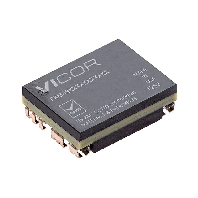
PRM48BH480x250A00
S
C
NRTL
US
High Efficiency Converter
Features
Product Ratings
• 48.0 V input (38.0 V to 55.0 V),
non-isolated ZVS buck-boost regulator
• 20.0 V to 55.0 V adjustable output range
VIN = 38.0 V to 55.0 V
POUT = 250 W
VOUT = 48.0 V
(20.0 V to 55.0 V Trim)
IOUT = 5.21 A
• 250 W output power in 0.57 in2 footprint
• 96.7% typical efficiency, at full load
• 1676 W/in3 (102 W/cm3) Power Density
• 5.29 MHrs MTBF (MIL-HDBK-217 Plus Parts Count)
• Pin selectable operating mode
Adaptive Loop
Remote Sense / Child
• Half VI Chip® Package
22.0mm x 16.5mm x 6.73mm
Typical Applications
•
•
•
•
•
High Density Power Supply DC-DC rail outputs
High Density ATE system DC-DC power
Telecom NPU and ASIC core power
Communications Systems
Non-isolated and isolated power converters
Product Description
The VI Chip® PRMTM Regulator is high e ciency converter,
operating from a 38.0 to 55.0 Vdc input to generate a regulated
20.0 to 55.0 Vdc output. The ZVS buck-boost topology enables
high switching frequency (~1.03 MHz) operation with high
conversion e ciency. High switching frequency reduces the
size of reactive components enabling power density up to
1676 W/in3.
The Half VI Chip® package is compatible with standard pickand-place and surface mount assembly processes with a planar
thermal interface area and superior thermal conductivity.
In a Factorized Power Architecture™ system, the PRM and
downstream VTMTM current multiplier minimize distribution
and conversion losses in a high power solution, providing an
isolated, regulated output voltage.
The PRM48BH480x250A00 has two selectable modes of
regulation depending on the application requirements.
In Adaptive Loop Operation, the PRM48BH480x250A00 utilizes
a unique feed-forward scheme that enables precise regulation
of an isolated POL voltage without the need for remote sensing
and voltage feedback.
In Remote Sense Operation, the internal regulation circuitry is
disabled, and an external control loop and current sensor
maintain regulation. This a ords flexibility in the design of both
voltage and current compensation loops to optimize
performance in the end application.
PRM™ Regulator
Page 1 of 42
Rev 1.7
11/2020
�PRM48BH480x250A00
Typical Applications
PRM
ENABLE
VAUX
SGND
RTRIM
RAL
VTM
REF/
REF_EN
TRIM
ON/OFF
CONTROL
AL
VT
SHARE/
CONTROL NODE
VC
VOUT
Adaptive Loop Temperature Feedback
+OUT
TM
VTM Start Up Pulse
VC
IFB
PC
+OUT
+IN
COUT
SGND
Vin
+IN
VF: 20 V to 55 V
CIN
–IN
SGND
LF
CF
–OUT
–IN
–OUT
PRIMARY
GND
SECONDARY
SEC_GND
ISOLATION BOUNDRY
SGND
Typical Application: PRM48BH480x250A00 + VTM Adaptive Loop Configuration
VREF
SGND
ENABLE
VAUX
SGND
SGND
SGND
OUT
Voltage Sense and Error Amplifier
(Differential)
GND
VTM
REF/
REF_EN
TRIM
ON/OFF
CONTROL
REF 3312
IN
AL
VT
SHARE/
CONTROL NODE
VC
SGND
TM
Voltage Reference with Soft Start
IFB
Voltage Sense
PRM
VTM Start up Pulse
V+
+OUT
VC
PC
V–
VOUT
+IN
VIN
+IN
LF
External Current Sense
–IN
SGND
COUT
SGND
+OUT
CIN
[1]
–IN
+IN
CF
–IN
–OUT
GND
–OUT
PRIMARY
SECONDARY
ISOLATION BOUNDRY
SGND
Typical Application: PRM48BH480x250A00 + VTM, non-isolated Remote Sense Configuration
[1]
Non-Isolated Configuration: –Out connected to -IN
PRM™ Regulator
Page 2 of 42
Rev 1.7
11/2020
GND
[1]
LOAD
�PRM48BH480x250A00
Pin Configuration
1
SHARE/
CONTROL NODE
A
TRIM
C
NC
E
TOP VIEW
2
B
ENABLE
D
NC
F
AL
3
VT
A
IFB
C
REF/REF_EN
E
4
B
VAUX
D
SGND
F
VC
+IN
G
G
+OUT
-IN
H
H
-OUT
Half VIC SMD
Pin Descriptions
Pin
Number
Signal Name
F4
SHARE
(Adaptive Loop / Child Operation)
CONTROL NODE
(Remote Sense Operation)
VT
(Adaptive Loop Operation)
ENABLE
VAUX
TRIM
IFB
(Remote Sense Operation)
NC
SGND
NC
REF
(Adaptive Loop Operation)
REF_EN
(Remote Sense Operation)
AL
(Adaptive Loop Operation)
VC
G1,G2
+IN
G3,G4
+OUT
H1,H2
-IN
H3,H4
-OUT
A1
A3
B2
B4
C1
C3
D2
D4
E1
E3
F2
PRM™ Regulator
Page 3 of 42
Type
BIDIR
INPUT
INPUT
BIDIR
OUTPUT
INPUT
INPUT
n/a
INPUT
n/a
Function
Parallel sharing control bus for parent-child configuration.
Modulator control node input. Driven by external error amplifier in Remote Sense
Operation.
VTM TM input for temperature compensation. Leave disconnected for Remote Sense
Operation.
Enables power supply when allowed to float high. 5 V during normal operation.
9 V auxiliary bias voltage.
Selects operating mode. Adjusts output voltage in Adaptive Loop Operation.
Current sense input for current limit and overcurrent protection in Remote Sense Operation.
Leave disconnected for Adaptive Loop Operation.
Do not connect this pin.
Signal ground, reference for analog controls. Kelvin connected internally to –IN and –OUT.
Do not connect this pin.
OUTPUT
Reference voltage for internal error amplifier in Adaptive Loop Operation.
OUTPUT
Powers and enables external control circuit voltage reference in Remote Sense Operation.
INPUT
OUTPUT
INPUT
POWER
OUTPUT
POWER
INPUT
POWER RETURN
OUTPUT
POWER RETURN
Adaptive loop gain control. Sets the magnitude of the Adaptive Loop load line in Adaptive
Loop Operation. Leave disconnected for Remote Sense Operation.
Bias voltage to power VTM module during start up
Positive input power terminal
Positive output power terminal
Negative input power terminal. Connected internally to -OUT.
Negative output power terminal. Connected internally to -IN.
Rev 1.7
11/2020
�PRM48BH480x250A00
Part Ordering Information
Device
Input Voltage
Range
Package Type
Output Voltage x 10
Temperature Grade
Output Power
Revision
Version
PRM
48B
H
480
T
250
A
00
PRM = PRM
48B = 38.0 V - 55.0 V
H = Half VIC
SMD
480 = 48.0 V
T = -40 to 125°C
M = -55 to 125°C
250 = 250 W
A
00 = AL / RS
Standard Models
Part Number
PRM48BH480T250A00
PRM48BH480M250A00
VIN
Package Type
VOUT
Temperature
38.0 V - 55.0 V
Half VIC
SMD
48.0 V
(20.0 V to 55.0 V)
-40 to 125°C
-55 to 125°C
Power
Version
250 W
AL / RS
(Pin Selectable)
Absolute Maximum Ratings
The ABSOLUTE MAXIMUM ratings below are stress ratings only. Operation at or beyond these maximum ratings can cause permanent damage to device.
Electrical specifications do not apply when operating beyond rated operating conditions. Operating beyond rated operating conditions for extended period of
time may affect device reliability. All voltages are specified relative to SGND unless otherwise noted. Positive pin current represents current flowing
out of the pin.
Parameter
Comments
Min
-0.3
SHARE / CONTROL NODE
-0.3
ENABLE
+IN to –IN
Continuous, non-operating
-1
100 ms, non-Operating
-0.5
VAUX
SGND
IFB
REF / REF _EN
Max
Unit
10.5
V
+/-10
mA
5.5
V
+/-10
mA
80
V
100
V
10.5
V
+/-100
mA
+/-100
mA
-0.5
5.7
V
-0.3
3.6
V
10
mA
Remote Sense Operation (REF _EN)
3.4
mA
TRIM
Adaptive Loop Operation (REF)
-0.3
3.6
V
AL
-0.3
3.6
V
VT
-0.3
4.8
V
-0.5
18
V
+/-1.8
A
VC to –OUT
+OUT to –OUT
-1
Output Current
62
V
7.3
A
Internal Operating
Temperature
T Grade
-40
125
°C
M Grade
-55
125
°C
Storage
Temperature
T Grade
-40
125
°C
M Grade
-65
125
°C
PRM™ Regulator
Page 4 of 42
Rev 1.7
11/2020
�PRM48BH480x250A00
Electrical Specifications
Specifications apply over all line and load conditions, and trim from 20.0 V to 55.0 V, unless otherwise noted; Boldface specifications apply over the
temperature range of -40ºC < TINT < 125ºC; All Other specifications are at TINT = 25ºC unless otherwise noted.
Attribute
Symbol
Conditions / Notes
Min
Typ
Max
Unit
38.0
0.001
48.0
55.0
1000
V
V/ms
V
ms
W
mA
A
µF
mΩ
Power Input Specification
Input Voltage Range
VIN Slew Rate
Initialization Voltage
Initialization Delay
No Load Power Dissipation
Input Quiescent Current
Input Current
Input Capacitance (Internal)
Input Capacitance (Internal) ESR
VIN
dVIN /dt
VINIT
tINIT
PNL
IQC
IIN_DC
CIN_INT
RCIN
Continuous, operating
0 ≤ VIN ≤ 55.0 V
Internal micro controller initialization voltage
From VIN first crossing VINIT
ENABLE HIGH, VIN = 48.0 V
ENABLE LOW, VIN = 48.0 V
IOUT = 5.21 A, VIN = 48.0 V, VOUT = 48.0 V
Effective value, VIN = 48.0 V (see Fig. 13)
Effective value, VIN = 48.0 V
5.0
10
7.0
2.4
14.5
5.4
2
3.0
9.0
3.5
20.0
5.6
Power Output Specification
Rated Output Current
IOUT
Standalone and Parent Operation, see Figure 1, SOA
5.21
A
Rated Output Power
POUT
250
W
1.07
MHz
Switching Frequency
FSW
Standalone and Parent Operation, see Figure 1, SOA
VIN = 48.0 V VOUT = 48.0 V,
IOUT = 2.60 A, TINT = 25°C
Over line, load, trim and temperature,
exclusive of burst mode
From VIN first crossing VIN_UVLO+_SUPV
to ENABLE high; tINIT expired
1.07
MHz
Output Turn-ON Delay
tON
0.94
0.70
From ENABLE pin release to ENABLE high, VIN applied, tOFF expired
Start up Sequence Timeout
Efficiency Ambient
Efficiency Hot
Efficiency Over Temperature
Output Discharge current
tSTARTUP_SEQ From ENABLE high to start up sequence complete
ηAMB
ηHOT
µs
20
µs
17
ms
95.7
96.7
%
VIN = 48.0 V, VOUT = 48.0 V, IOUT = 2.60 A, TINT = 25°C
94.7
95.7
%
VIN = 38.0 V to 55.0 V,
VOUT = 48.0 V, IOUT = 5.21 A, TINT = 25°C
VIN = 38.0 V to 55.0 V,
IOUT = 5.21 A, TINT = 25°C, over trim
VIN = 48.0 V, VOUT = 48.0 V,
IOUT = 5.21 A, TINT = 100°C
VIN = 48.0 V, VOUT = 48.0 V,
IOUT = 2.60 A, TINT = 100°C
VIN = 38.0 V to 55.0 V , VOUT = 48.0 V,
IOUT = 5.21 A, TINT = 100°C
VIN = 38.0 V to 55.0 V , IOUT = 5.21 A,
TINT = 100°C, over trim
95.0
%
92.0
%
95.5
96.5
%
94.5
95.8
%
95.0
%
91.5
%
η
>50% load and VOUT = 48.0 V; over temperature
94.5
%
>50% load; over temperature and trim
89.0
%
IOD
Average Value
VIN = 48.0 V, VOUT = 48.0 V,
IOUT = 5.21 A, COUT_EXT = 0 F, 20 MHz BW
VOUT_PP
Output Inductance (Parasitic)
LOUT_PAR
Frequency @ 1.03 MHz, Simulated J-Lead model
Output Capacitance (Internal)
COUT_INT
Effective value, VOUT = 48.0 V (see Fig.13)
PRM™ Regulator
Page 5 of 42
20
VIN = 48.0 V, VOUT = 48.0 V, IOUT = 5.21 A, TINT = 25°C
Output Voltage Ripple
Output Capacitance (Internal) ESR
1.03
RCOUT
Effective value, VOUT = 48.0 V
Rev 1.7
11/2020
0.5
1000
2.5
mA
1500
mV
nH
2
µF
3.0
mΩ
�PRM48BH480x250A00
Electrical Specifications (cont.)
Specifications apply over all line and load conditions, and trim from 20.0 V to 55.0 V, unless otherwise noted; Boldface specifications apply over the
temperature range of -40ºC < TINT < 125ºC; All Other specifications are at TINT = 25ºC unless otherwise noted.
Attribute
Symbol
Conditions / Notes
Min
Typ
Max
Unit
47.00
20.0
1.7
48.00
49.00
55.0
1.9
0.2
0.2
0.2
V
V
ms
%
%
%
3
%
5
%
7.3
A
7.29
A
47
µF
25
µF
4.8
V
Power Output Specifications: Adaptive Loop Operation
Output Voltage Setpoint
Output Voltage Trim Range
Output Voltage Rise Time
Output Voltage Load Regulation
Output Voltage Line Regulation
Total Regulation Error
Total AL Regulation Error
Output Current Limit
VOUT_SET
VOUT
tRISE_VOUT
From soft start initiated to output voltage settled
VOUT_REG_LOAD Adaptive loop load line inactive
VOUT_REG_LINE Adaptive loop load line inactive
VOUT_REG_TOTAL PRM output voltage, Adaptive Loop load line inactive
VOUT_REG_AL
ILIMIT
Load Capacitance (Electrolytic)
CLOAD_ALEL
Load Capacitance (Ceramic)
CLOAD_CER
Load Transient Voltage Deviation
Load Transient Recovery Time
No load, trim Inactive, Adaptive Loop load line inactive
VTRANS
tTRANS
VTM output voltage, total Adaptive Loop regulation,
VOUT = 48.0 V, trim inactive
Rated Power Within an Array
Current Sharing Difference
(Parent to Child)
PRM™ Regulator
Page 6 of 42
IOUT_ARRAY
POUT_ARRAY
IOUT_SHARE_MS
1
VTM output voltage, total Adaptive Loop regulation,
trim active, exclusive of external resistor tolerances
VIN = 48.0 V, VOUT = 48.0 V, TINT = 25°C, constant
current limit after supervisory limit detection time tLIM_SUPV
5.7
Over line, load, trim and temperature
5.2
0.1 Ω ≤ ESR ≤ 1 Ω, See Figure 32,
total capacitance (CLOAD_ALEL + CLOAD_CER) ≤ 47 µF
6.5
2 mΩ ≤ ESR ≤ 200 mΩ, See Figure 32
10% ↔ 100% load step, 10 A/µsec, 0 µF COUT,
deviation from initial setpoint
10% ↔ 100% load step, 10 A/µsec, 0 µF COUT,
Recovery to 90% of final value, Adaptive Loop
load line inactive
10% ↔ 100% load step, 10 A/µsec, 0 µF COUT,
Recovery to 90% of final value,
Adaptive Loop load line active, VAL = 0.96 V
Power Output Specifications: Child Operation with AL Parent
Child Operation within an array, up to 5°C case
Rated Current Within an Array
1.8
0.02
0.02
temperature differential, parent-child configuration
Child Operation within an array, up to 30°C case
temperature differential, parent-child configuration
Child Operation within an array, up to 5°C case
temperature differential, parent-child configuration
Child Operation within an array, up to 30°C case
temperature differential, parent-child configuration
Equal input, and output voltage at full load;
VIN = 48.0 V, VOUT = 48.0 V
Equal input and output voltage at full load;
Over line and trim, with 25°C ≤ TC ≤ 100°C and ≤ 5°C
part-part temp. mismatch
Equal input, and output voltage at full load;
Over line and trim, with 25°C ≤ TC ≤ 100°C
and ≤ 30°C part-part temp. mismatch
Rev 1.7
11/2020
100
µs
500
µs
4.2
A
3.6
A
200
W
175
W
15
%
15
%
20
%
�PRM48BH480x250A00
Electrical Specifications (cont.)
Specifications apply over all line and load conditions, and trim from 20.0 V to 55.0 V, unless otherwise noted; Boldface specifications apply over the
temperature range of -40ºC < TINT < 125ºC; All Other specifications are at TINT = 25ºC unless otherwise noted.
Attribute
Symbol
Conditions / Notes
Min
Power Output Specifications: Child Operations (cont.)
Equal input, output, and SHARE voltage at full load;
Current Sharing Difference
(Child to Child)
Maximum Array Size
Output Voltage Range
Rated Current Within an Array
Rated Power Within an Array
Current Sharing Difference
Maximum Array Size
PRM™ Regulator
Page 7 of 42
IOUT_SHARE_SS
NPRMS_PARALLEL
VIN = 48.0 V, VOUT = 48.0 V
Equal input, output and SHARE voltage at full load;
Over line and trim, with 25°C ≤ TC ≤ 100°C
and ≤ 5°C part-part temp. mismatch
Equal input, output, and SHARE voltage at full load;
Over line and trim, with 25°C ≤ TC ≤ 100°C
and ≤ 30°C part-part temp. mismatch
Maximum number of parallel devices,
parent-child configuration
Power Output Specifications: Remote Sense Operation
VOUT
Remote Sense Operation within an array,
up to 5°C case temperature differential
IOUT_ARRAY
Remote Sense Operation within an array,
up to 30°C case temperature differential
Remote Sense Operation within an array,
up to 5°C case temperature differential
POUT_ARRAY
Remote Sense Operation within an array,
up to 30°C case temperature differential
Equal input, output, and CONTROL NODE voltage
at full load; VIN = 48.0 V, VOUT = 48.0 V
Equal input, output and CONTROL NODE voltage at
full load; Over line and trim, with 25°C ≤ TC ≤ 100°C
IOUT_SHARE_RS and ≤ 5°C part-part temp. mismatch
Equal input, output, and CONTROL NODE voltage at
full load; Over line and trim,
with 25°C ≤ TC ≤ 100°C and ≤ 30°C
part-part temp. mismatch (worst case)
Maximum number of parallel devices, Remote Sense
NPRMS_PARALLEL
configuration, CONTROL NODE externally driven
Rev 1.7
11/2020
20.0
Typ
Max
Unit
5
%
10
%
15
%
5
PRMs
55.0
V
4.7
A
4.2
A
225
W
202
W
5
%
10
%
15
%
10
PRMs
�PRM48BH480x250A00
Electrical Specifications (cont.)
Specifications apply over all line and load conditions, and trim from 20.0 V to 55.0 V, unless otherwise noted; Boldface specifications apply over the
temperature range of -40ºC < TINT < 125ºC; All Other specifications are at TINT = 25ºC unless otherwise noted.
Attribute
Symbol
Conditions / Notes
Min
Typ
Max
Unit
24.5
22.7
2.2
62.6
63.6
1.0
57.9
26.0
8.8
9.5
7.2
V
V
V
V
V
V
V
V
ºC
W
V
V
V
6.9
V
5
ms
75
ms
Powertrain Protections
Input Undervoltage Turn-ON
Input Undervoltage Turn-OFF
Input Undervoltage Hysteresis
Input Overvoltage Turn-ON
Input Overvoltage Turn-OFF
Input Overvoltage Hysteresis
Output Overvoltage Threshold
Minimum Current Limited Vout
Overtemperature Shutdown Setpoint
Output Power Limit
Short Circuit VOUT Threshold
Short Circuit VOUT Recovery Threshold
Short Circuit CONTROL NODE Threshold
Short Circuit CONTROL NODE
Recovery Threshold
VIN_UVLO+
VIN_UVLOVUVLO_HYST
VIN_OVLOVIN_OVLO+
VOVLO_HYST
VOUT_OVP+
VOUT_UVP
TINT_OTP
PPROT
VSC_VOUT
VSC_VOUTR
VSC_VCN
Instantaneous powertrain shutdown, detected after tBLANK
(VIN_UVLO+) - (VIN_UVLO-)
Instantaneous powertrain shutdown, detected after tBLANK
(VIN_OVLO+) - (VIN_OVLO-)
Instantaneous shutdown, detected after tPROT
Instantaneous shutdown, detected after tPROT
22.0
1.8
56.0
0.7
56.0
tSC
Short Circuit Recovery Time
Overcurrent (IFB) and
Input Over/Undervoltage Blanking Time
Overtemperature, Output Overvoltage
and ENABLE Shutdown Response Time
(Hardware)
tSCR
Short circuit fault detected after VSC_VOUT
and VSC_VCN thresholds persist for this time
Excludes tOFF
50
tBLANK
67.3
1.4
60.0
12
125
250
VSC_VCNR
Short Circuit Timeout
2.5
tPROT
120
150
2
µs
µs
Powertrain Supervisory Limits
Input Undervoltage Turn-ON
(Supervisory)
Input Undervoltage Turn-OFF
(Supervisory)
Input Undervoltage Hysteresis
(Supervisory)
Input Overvoltage Turn-ON
(Supervisory)
Input Overvoltage Turn-OFF
(Supervisory)
Input Overvoltage Hysteresis
(Supervisory)
Undertemperature Shutdown Setpoint
(Supervisory)
Supervisory Limit Response Time
PRM™ Regulator
Page 8 of 42
VIN_UVLO+_SUPV
VIN_UVLO-_SUPV
35.8
Powertrain shutdown, detected after tLIM_SUPV
VUVLO_HYST_SUPV (VIN_UVLO+_SUPV) - (VIN_UVLO-_SUPV)
VIN_OVLO-_SUPV
VIN_OVLO+_SUPV
33.6
1.9
2.2
56.0
57.7
Powertrain shutdown, detected after tLIM_SUPV
VOVLO_HYST_SUPV (VIN_UVLO+_SUPV) - (VIN_UVLO-_SUPV)
TINT_UTP
32.2
T Grade
M Grade
tLIM_SUPV
Rev 1.7
11/2020
0.8
37.0
V
V
2.5
V
V
58.9
60.0
V
1.2
1.7
V
-40
-55
150
ºC
ºC
µs
�PRM48BH480x250A00
Signal Specifications
Specifications apply over all line and load conditions, TINT = 25ºC and output voltage from 20.0 V to 55.0 V, unless otherwise noted.
Boldface specifications apply over the temperature range of -40ºC < TINT < 125ºC (T-grade).
ENABLE
• The ENABLE pin enables and disables the PRM
• In PRM array configurations, ENABLE pins should be connected in order to synchronize start up
• ENABLE is 5 V with 1.8 mA source capability during normal operation
Signal Type
State
Normal
Analog Output
Operation
Start up
Start up
Attribute
Symbol
ENABLE Voltage
VENABLE
ENABLE Current
IENABLE_OP
ENABLE Source Current
IENABLE_EN
Minimum Time to Start
tOFF
ENABLE
ENABLE
Standby
Max
Unit
5.0
5.3
V
1.8
mA
90
13.0
RENABLE_EXT
Resistance (External)
Fault
Typ
4.7
After tOFF
0.97
VENABLE_DIS
Disable Threshold
ENABLE
Digital Output
Min
VENABLE_EN
Enable Threshold
Digital Input / Output
Conditions / Notes
ENABLE
Sink Current to SGND
IENABLE_FAULT
µA
15.0
17.0
ms
2.5
3.2
V
2.40
Resistance to SGND required
V
235
Ω
4
mA
to disable the PRM
ENABLE voltage 1 V or above
VAUX: Auxillary Voltage Source
• Intended to power auxiliary circuits
• 9 V during normal operation with 5 mA source capability
Signal Type
State
Normal
Attribute
Symbol
VAUX Voltage
VVAUX
VAUX Current
IVAUX
Conditions / Notes
Min
Typ
Max
Unit
8.6
9.0
9.5
V
5
mA
400
mV
0.04
µF
IOUT = 0A, CVAUX_EXT = 0. Maximum
Operation
VAUX Voltage Ripple
VVAUX_PP
specification includes powertrain
Analog Output
100
operation in burst mode.
VAUX Capacitance
Transition
(External)
VAUX Fault Response
Time
CVAUX_EXT
From fault recognition to
tFR_VAUX
30
µs
VAUX = 1.5 V
VC: VTM Control
• Pulsed voltage source used to power and synchronize downstream VTM during start up
• 14 V, 10 ms typical voltage pulse
Signal Type
State
Attribute
VC Voltage
Analog Output
Start up
VC Available Current
VC Duration
VC Slew Rate
Symbol
Conditions / Notes
VVC_START
IVC_START
Connected to VTM VC or equivalent,
PRM™ Regulator
Page 9 of 42
Typ
Max
Unit
13
14
18
V
IVC = 115 mA, CVC = 3.2 uF
VC = 14 V, VIN > 20 V
200
7
tVC
Connected to VTM or equivalent,
dVC/dt
IVC = 115 mA, CVC = 3.2 uF
ENABLE to VC Delay
Min
tENABLE-VC
Rev 1.7
11/2020
mA
10
0.02
20
16
ms
0.25
V/µs
µs
�PRM48BH480x250A00
Signal Specifications (cont.)
Specifications apply over all line and load conditions, TINT = 25ºC and output voltage from 20.0 V to 55.0 V, unless otherwise noted.
Boldface specifications apply over the temperature range of -40ºC < TINT < 125ºC (T-grade).
SGND: Signal Ground
• All control signals must be referenced to this pin, with the exception of VC
• SGND is internally connected to -IN and -OUT
Signal Type
Analog Input / Output
State
Any
Attribute
Maximum Allowable
Current
Symbol
Conditions / Notes
Min
Typ
-100
ISGND
Max
Unit
100
mA
TRIM
• TRIM is used to select operating mode and trim the output voltage in Adaptive Loop Operation
• Internal pullup to VCC_INT through 10 kΩ resistor
• When pulled below 0.45 V during power up, Remote Sense / Child Operation is selected
• When allowed to pull up above 0.55 V during power up, Adaptive Loop Operation is selected
• Operating mode is detected during power up and cannot be changed unless input power is cycled
Signal Type
State
Attribute
Internally Generated
Normal
Operation
VCC
Internal Pullup
Resistance to VCC_INT
Analog Input
Mode Detection
Delay
Mode
Remote Sense
Detect
Enable Threshold
Remote Sense
Disable Threshold
Symbol
Conditions / Notes
VCC_INT
RTRIM_INT
0.5% tolerance resistor
tMODE_DETECT
From ENABLE high to mode detected,
VRS_MODE_EN
after VIN first applied
Pull below this value during first
start up after application of power
to enable Remote Sense / Child
Operation
Pull above this value during first
VRS_MODE_DIS
start up after application of power to
enable Adaptive Loop Operation
PRM™ Regulator
Page 10 of 42
Rev 1.7
11/2020
Min
Typ
Max
Unit
3.20
3.28
3.36
V
9.83
10.00
10.18
kΩ
100
140
200
µs
0.45
V
0.55
V
�PRM48BH480x250A00
Signal Specifications (cont.)
Specifications apply over all line and load conditions, TINT = 25ºC and output voltage from 20.0 V to 55.0 V, unless otherwise noted.
Boldface specifications apply over the temperature range of -40ºC < TINT < 125ºC (T-grade).
TRIM (Adaptive Loop Operation Only)
• Provides dynamic trim control over the PRM output voltage in Adaptive Loop Operation
• Sampled prior to every start up to detect if trim is active or inactive
• Output voltage is equal to 20 times the voltage at the TRIM pin when applied TRIM voltage is within the active range
• Trim state is detected during normal operation and cannot be changed until start up is initiated
Signal Type
State
Attribute
Symbol
Conditions / Notes
Min
Start up
Trim Enable Threshold
VTRIM_EN
Trim Disable Threshold
VTRIM_DIS
Minimum Trim Disable
Resistance
Trim Capacitance
(External)
Trim Sample Delay
Analog Input
TRIM Pin
Analog Range
TRIM Gain
Pull below this value during
start up to enable trim control
PRM™ Regulator
Page 11 of 42
Trim Accuracy
Minimum TRIM resistance required
to disable trim
3.20
10
From ENABLE high to TRIM sampled
100
VTRIM_RANGE
See Figure 26
1.00
VOUT / VTRIM,
GTRIM
%ACC_TRIM
VOUT Referred
Trim Resolution
VOUT_RES
Trim Latency
tTRIM_LAT
Trim Bandwidth
BWTRIM
140
100
pF
200
µs
2.75
V
20
VTRIM applied within active range
Vout accuracy, exclusive of
0.5
external resistor tolerance
V/V
2.0
200
60
-3dB point
Rev 1.7
11/2020
V
MΩ
CTRIM_EXT
tENABLE_TRIM
Unit
V
start up to disable trim control
RTRIM_DIS_MIN
Max
3.10
Pull above this value during
Normal
Operation
Typ
120
1.2
%
mV
240
µs
kHz
�PRM48BH480x250A00
Signal Specifications (cont.)
Specifications apply over all line and load conditions, TINT = 25ºC and output voltage from 20.0 V to 55.0 V, unless otherwise noted.
Boldface specifications apply over the temperature range of -40ºC < TINT < 125ºC (T-grade).
AL: Adaptive Loop (Adaptive Loop Operation Only)
• Provides Adaptive Loop load line programming in Adaptive Loop Operation
• Internal pullup to VCC_INT through 10 kΩ resistor
• Sampled prior to every start up to detect if Adaptive Loop load line is active or inactive
• Leave open to disable Adaptive Loop load line
• Not used in Remote Sense Operation
Signal Type
State
Attribute
Symbol
Conditions / Notes
Start up
AL Enable Threshold
VAL_EN
AL Disable Threshold
VAL_DIS
Minimum AL Disable
Resistance
AL Capacitance
(External)
AL Sample Delay
Internally generated
Analog Input
VCC
Internal Pullup
Resistance to VCC_INT
Normal
Operation
AL Pin Analog Range
AL Gain
Pull below this value during start up
to enable AL load line
Maximum Output
Referred Compensation
PRM™ Regulator
Page 12 of 42
Typ
Minimum AL resistance required
to disable AL load line
3.20
10
From ENABLE high to AL sampled
VCC_INT
RAL_INT
0.5% tolerance resistor
GAL
200
µs
3.20
3.28
3.36
V
9.83
10.00
10.18
kΩ
Positive correction slope, VT inactive
AL Bandwidth
BWAL
3.10
1.0
Full load slope accuracy exclusive
0.5
of external resistor tolerance
2.0
3
VOUT_AL_MAX
tAL_LAT
pF
140
LLAL_RES
AL Latency
100
100
0
VAL_RANGE
Maximum increase from no
load setpoint, VOUT ≤ 55.0 V
60
-3dB point
Rev 1.7
11/2020
V
MΩ
CAL_EXT
tENABLE_AL
Unit
V
to disable AL load line
RAL_DIS_MIN
Max
3.10
Pull above this value during start up
AL Load Line Accuracy %ACC_LL_AL
AL Load Line Resolution
Min
120
1.2
V
Ω/V
%
mΩ
5
V
240
µs
kHz
�PRM48BH480x250A00
Signal Specifications (cont.)
Specifications apply over all line and load conditions, TINT = 25ºC and output voltage from 20.0 V to 55.0 V, unless otherwise noted.
Boldface specifications apply over the temperature range of -40ºC < TINT < 125ºC (T-grade).
VT: VTM Temperature (Adaptive Loop Operation Only)
• VTM temperature compensation for Adaptive Loop regulation
• Adjusts the slope of the Adaptive Loop load line to account for changes in VTM output resistance over temperature
• Connect to TM pin of compatible downstream VTM to enable temperature compensation
• Leave disconnected to disable temperature compensation
Signal Type
State
Attribute
Symbol
Conditions / Notes
Min
Internal Resistance
to SGND
VT Enable Threshold
VT Disable Threshold
VT Disable Default
Analog Input
Normal
Operation
Temperature
VT Analog Range
VT Temperature
Coefficient
VT Resolution
RVT_INT
temperature compensation
2.18
VT within active range, referenced
TCVT
to 2.98 V
VTM TM voltage applied, .01V/°K,
TCVT
referenced to 25°C
TCVT_RES
BWVT
VTM TM voltage applied, .01V/°K
-3dB point
REF: Reference (Adaptive Loop Operation Only)
• Functions as REF pin in Adaptive Loop Operation
• REF represents the internal voltage reference for the voltage control circuit
• VOUT approximately equal to 20 times REF voltage
Signal Type
State
Attribute
Symbol
Conditions / Notes
REF to VOUT
Normal
Operation
Analog Output
Scale Factor
REF Resistance
(External)
REF Capacitance
(External)
REF Voltage Ripple
ENABLE to REF Delay
Transition
PRM™ Regulator
Page 13 of 42
VAUX to REF Delay
VREF
GREF_VOUT
3.98
30
%/V
0.3
%/C
120
°C
240
1.5
Min
Typ
Max
Unit
2.4
V
VOUT / VREF
20
V/V
MΩ
200
CREF_EXT
tENABLE_REF
µs
kHz
10
VREF_PP
V
VOUT = 48.0 V, trim inactive
RREF_EXT
tVAUX_REF
°C
0.4
60
V
V
25
when VT disabled
VVT_OP
Bandwidth
1.9
Default AL temperature setting
TVT_DIS
Unit
kΩ
2.1
Pull below this value to disable VT
VVT_DIS
tVT_LAT
Max
80.4
VVT_EN
VT Latency
REF Voltage
Typ
pF
Includes burst mode, 20 MHz BW
25
mV
ENABLE low to REF low
120
µs
1
ms
VAUX = 8.1 V to REF soft start
ramp initiated
Rev 1.7
11/2020
�PRM48BH480x250A00
Signal Specifications (cont.)
Specifications apply over all line and load conditions, TINT = 25ºC and output voltage from 20.0 V to 55.0 V, unless otherwise noted.
Boldface specifications apply over the temperature range of -40ºC < TINT < 125ºC (T-grade).
REF_EN: Reference Enable (Remote Sense and Child Operation Only)
• Functions as REF_EN pin in Remote Sense and Child Operation
• REF_EN signals successful start up and powertrain ready to operate
• Intended to power and enable the external feedback circuit reference in Remote Sense Operation
• 3.25 V, 4 mA regulated voltage source
Signal Type
State
Attribute
Symbol
Conditions / Notes
Min
Typ
Max
Unit
2.72
3.25
3.37
V
50
100
Ω
IREF_EN
4
mA
CREF_EN_EXT
0.1
µF
REF_EN Voltage
REF_EN Source
Normal
Operation
Analog Output
Impedance
REF_EN Current
REF_EN Capacitance
(External)
REF_EN Voltage Ripple
ENABLE to REF_EN
Transition
Delay
VAUX to REF_EN
Delay
VREF_EN
REF_EN unloaded
ROUT_REF_EN
VREF_EN_PP
Includes burst mode, 20 MHz BW
25
mV
tENABLE_REF_EN
ENABLE low to REF_EN low
120
µs
tVAUX_REF_EN
VAUX = 8.1 V to REF_EN high
1
ms
Share (Adaptive Loop and Child Operation Only)
• Functions as SHARE pin in parent child array configuration
• Current share bus for array operation (parent/child scheme)
• Sources current and provides SHARE signal in parent operation
• Sinks constant current when externally driven in active range (Child Operation)
Signal Type
State
Attribute
Symbol
Conditions / Notes
SHARE Voltage
Standalone/
Analog Output
Parent
Operation
Active Range
SHARE Available
Current
SHARE Resistance
to SGND
Analog Input
PRM™ Regulator
Page 14 of 42
Child
Operation
SHARE Sink Current
Min
Typ
0.79
VSHARE
ISHARE
VSHARE > 0.79 V
Max
Unit
7.40
V
2.5
RSHARE
mA
93.3
ISHARE_SINK
VSHARE > 0.79 V
Rev 1.7
11/2020
0.25
0.50
kΩ
0.75
mA
�PRM48BH480x250A00
Signal Specifications (cont.)
Specifications apply over all line and load conditions, TINT = 25ºC and output voltage from 20.0 V to 55.0 V, unless otherwise noted.
Boldface specifications apply over the temperature range of -40ºC < TINT < 125ºC (T-grade).
Control Node (Remote Sense Operation Only)
• Functions as CONTROL NODE pin in Remote Sense Operation
• Modulator control node voltage sets power train timing
• Driven by external error amplifier in Remote Sense Operation
• Sinks constant current when externally driven in active range
• Sources current, and clamps voltage to 0.79 V when pulled below active range
Signal Type
State
Attribute
Symbol
Conditions / Notes
CONTROL NODE
Voltage Active Range
CONTROL NODE
Analog Input
Normal
Operation
Source Current
CONTROL NODE
Sink Current
CONTROL NODE
Resistance to SGND
Min
Typ
0.79
VCN
ICN_LOW
VCN < 0.79 V
ICN_SINK
VCN > 0.79 V
0.25
RCN
0.50
Max
Unit
7.40
V
2.5
mA
0.75
mA
93.3
kΩ
IFB: Current Feedback (Remote Sense Operation Only)
• Functions as IFB pin in Remote Sense Operation
• A voltage proportional to the PRM output current must be supplied externally to the IFB pin in order for the device to properly protect overcurrent events
and to enable output current limit (clamp)
• Overcurrent protection trip will cause instantaneous powertrain disable, detected after tBLANK
• Not used for Adaptive Loop Operation
Signal Type
State
Attribute
Symbol
Conditions / Notes
Min
Typ
Max
Unit
Current Limit (Clamp)
Threshold
Analog Input
Normal
Operation
VIN = 48.0 V; VOUT = 48.0 V
VIFB_IL
Over line, trim, and temperature
Not production tested; guaranteed
Overcurrent
Protection
TINT = 25°C
VIFB_OC
Threshold
by design; TINT = 25°C
1.90
2.00
1.85
2.58
2.69
2.10
V
2.15
V
2.80
V
2.82
V
2.17
kΩ
Not production tested; guaranteed
by design; over line, trim,
2.56
and temperature
IFB Input Impedance
RIFB
Current Limit
Bandwidth
BWIL
2.09
2.0
NC: No Connect
• Reserved for factory use only
• No connections should be made to these pins
PRM™ Regulator
Page 15 of 42
2.13
Rev 1.7
11/2020
kHz
�PRM48BH480x250A00
Functional Block Diagram
+IN
+OUT
Q3
Q1
COUT
CIN
L
-IN
-OUT
Q2
Q4
PGND
Internal
VCC
Regulator
30.1 kΩ
VCC
Modulator
2.5 mA Min
Error Amplifier
3.3 V
Linear
Regulator
0.5 mA
Voltage Reference
3.3 V
SHARE/
CONTROL NODE
1.58 kΩ
OTP
Enable
10
kΩ
VT
10
kΩ
2.1 kΩ
ENABLE
10 kΩ
20 kΩ
TRIM
0.01 uF
NC
Control and Monitoring
1000 pF
NC
Overvoltage
Lockout
Undervoltage
Lockout
10 kΩ
0.01 uF
Current
Limit
1000 pF
Output
Short
Circuit
35.7 kΩ
IN
Adaptive
Loop
SGND
SGND
PRM™ Regulator
Page 16 of 42
PGND
Rev 1.7
11/2020
SGND
REF/
REF_EN
60.4
kΩ
10
kΩ
6800
pF
OUT
IFB
30.1kΩ
0.01 uF
Output
Overvoltage
Protection
AL
57.6 kΩ
VAUX
VC
2200
pF
�PRM48BH480x250A00
High Level Functional State Diagram
Conditions that cause state transitions are shown along arrows. Sub-sequence activities listed inside the state bubbles.
Application of
Vin
VIN > UVLO+
STARTUP SEQUENCE
STANDBY SEQUENCE
tON expired
ENABLE: 1.8mA to HIGH
VC Pulse
REF_EN active
ENABLE rising edge
ENABLE: 10uA to LOW
tOFF expired
ENABLE: 90uA to HIGH
Adaptive loop and trim modes latched
RS mode latched at first ENABLE
after Vin applied only
Powertrain Stopped
ENABLE falling edge,
Output OVP,
or OTP detected
Powertrain Active
Input OVLO or UVLO,
Output UVP,
or UTP detected
Fault
Autorecovery
ENABLE falling edge,
Output OVP or
OTP detected
FAULT SEQUENCE
ENABLE pulsed: 25mA to
LOW
Input OVLO or UVLO,
Output UVP,
or UTP detected
Powertrain Stopped
SUSTAINED
OPERATION
ENABLE: 1.8mA to HIGH
Powertrain Active
Short Circuit detected
PRM™ Regulator
Page 17 of 42
tSTARTUP_SEQ
expired
Rev 1.7
11/2020
�PRM™ Regulator
Page 18 of 42
Rev 1.7
11/2020
AL
TRIM
2.4V
20V
48V
55V
tAUX_REF
TRIM Ignored
2
TRIM
INACTIVE
TRIM and AL pins
sampled
Soft Start
tVC
tENABLE_VC
tOFF tON
Micro controller
initialized
1V
0V
1.0V
3.3V
2.75V
VAUX
VAUX
VREF
VOUT_MIN
OUT_NOM
VOUTV
VOUT_OVP+
VOUT_MAX
VC
VVC_START
VENABLE_EN
ENABLE
OUTPUT
INPUT
ILIMIT
VENABLE
Iout
VSHARE_MIN
SHARE
REF
INPUT
VINIT
VSHARE_MAX
+IN
VIN_UVLO
VIN_OVLO
OUTPUT
OUTPUT
OUTPUT
BIDIR
BIDIR
BIDIR
INPUT
1
INPUT POWER ON
AND UV TURN ON
AL = 1V
3
AL
ACTIVE
FirstEnb: TR not low = not RS mode
TR high = trim inactive for this enabled period
AL not high = AL active for this enabled period
Vout increases by
VAL * GAL * IOUT
tBLANK
tBLANK
tBLANK
4
INPUT
OV
tOFF
Soft Start
5
INPUT OV
RECOVERY
TR high = trim inactive for this enabled period
AL not high = AL active for this enabled period
tPROT
tPROT
8
9
FULL LOAD OUTPUT
APPLIED
OV
Current sense activated, and output
increase due to AL after tSTARTUP_SEQ
expires
AL = 1V
tSTARTUP_SEQ
tON
6
7
ENABLE ENABLE
DISABLE RELEASE
TR high = trim inactive for this enabled period
AL not high = AL active for this enabled period
PRM48BH480x250A00
Timing Diagrams (Adaptive Loop Operation)
Module Inputs are shown in blue; Module Outputs are shown in brown.
�PRM™ Regulator
Page 19 of 42
Rev 1.7
11/2020
ILIMIT
VOUT
INPUT
1V
3.3V
1V
1V
2.4V
2.75V
20V
48V
55V
tBLANK
AL pin Ignored
VOUT = VTRIM * 20
Micro controller
Opera ng Mode
ini alized Trim and AL state detected
AL
TRIM 2.75V
2.4V
INPUT
3.3V
VAUX
OUTPUT
VAUX
REF
VOUT_MIN
VOUT_NOM
VOUT_MAX
VC
VVC_START
VENABLE_EN
ENABLE
VENABLE
Iout
VSHARE_MIN
SHARE
VSHARE_MAX
VINIT
VIN_UVLO
+IN
VIN_OVLO
OUTPUT
OUTPUT
OUTPUT
BIDIR
BIDIR
BIDIR
INPUT
tSC
tSCR+tOFF
FirstEnb: TR not low = not RS mode
TR not high = trim ac ve for this enabled period
AL high = AL inac ve for this enabled period
10
11
12
INPUT POWER ON
AL
OUTPUT
AND UV TURN ON
INACTIVE AND SHORT
TRIM
CIRCUIT
ACTIVE
tOFF
14
OT SHUTDOWN
AND RECOVERY
AL ac ve
Vout increase due to Iout and AL
a!er tSTARTUP_SEQ expires
VOUT clamped to 55V
for VTRIM > 2.75V
tSTARTUP_SEQ
13
ENABLE
TOGGLING
15
OUTPUT
POWER LIMIT
PROTECTION
tLIM_SUPV
16
CURRENT
LIMIT
EVENT
tBLANK
17
INPUT POWER OFF
AND
UV TURN OFF
TR high = trim inac ve for this enabled period
AL not high = AL ac ve for this enabled period
TR high = trim inac ve for this enabled period
AL not high = AL ac ve for this enabled period
TR not high = trim ac ve for this enabled period
AL high = AL inac ve for this enabled period
PRM48BH480x250A00
Timing Diagrams (Adaptive Loop Operation) (cont.)
Module Inputs are shown in blue; Module Outputs are shown in brown.
�PRM™ Regulator
Page 20 of 42
VINIT
VIN_UVLO
VENABLE
VIFB_IL
Rev 1.7
11/2020
TRIM
VAUX
tVC
tAUX_REF_EN
tOFF tON
Micro controller
ini alized
VAUX
VREF_EN
REF_EN
VOUT
VOUT_OVP+
VC
VVC_START
VENABLE_EN
ENABLE
IFB
VIFB_OC
VCN_MIN
CONTROL
NODE
VCN_MAX
+IN
VIN_OVLO
1
INPUT POWER ON AND UV
TURN ON
tBLANK
tENABLE_REF_EN
tBLANK
4
INPUT OV
RECOVERY
tENABLE_REF_EN
tPROT
5
ENABLE
DISABLE
6
ENABLE
RELEASE
tON
TRIM ignored for all subsequent
start up events un l VIN is removed
This blue shaded region is where trim voltage is a don’t care.
RS opera ng mode is latched. TRIM is ignored un l Vin is
removed.
t < tBLANK
tBLANK
2
3
QUICK OC INPUT OV
(t 45º: for the closed loop response, the phase
should be greater than 45º where the gain crosses 0 dB.
2 ʌu
2) Gain Margin > 10dB : The closed loop gain should be lower than 10dB where the phase crosses 0º.
n
3) Gain Slope = -20dB/decade : The closed loop gain should have a
slope of -20dB/decade at the crossover frequency.
rEQ _ OUT u RLOAD
rEQ _ OUT
RLOAD
rEQ _ OUT u RLOAD
rEQ _ OUT
RLOAD
Compensation Mid-Band Gain:
G MB � 20 log
The compensation characteristics must be selected to meet these
stability criteria. Refer to Figure 37 for a local sense, voltage-mode
control example based on the configuration in Figure 36. In this
example, it is assumed that the maximum crossover frequency
(FCMAX) has been selected to occur between B and C. Type-2
compensation (Curve IJKL) is sufficient in this case.
n
The following data must be gathered in order to proceed:
n
n Powertrain equivalent resistance rEQ: See Figures 18, 19, 20
n Internal output capacitance: see Figure 13
In the case of ceramic capacitors, the ESR can be considered low
enough to push the associated zero well above the frequency of
interest. Applications with high ESR capacitor may require a
different type of compensation, or cascade control.
(8)
1
2 ʌu R 3 u C1
(9)
Compensation Pole:
FP 2 �
n External output capacitance value
R3
R1
Compensation Zero:
FZ1 �
n Modulator Gain GCN: See Figures 18, 19, 20
u �COUT _ INT
COUT _ EXT
1
R3 u C1 u C2
2 ʌu
C1
C2
and for FP2>>FZ1 (C1 + C2 ≈ C1):
FP 2 5
1
2/ u R3 u C2
(10)
Open Loop Gain vs. Frequency
80
Gain (dB)
60
40
20
I
Application's op-amp
· G-
B
Compensation Gain
F
E
PRM Open Loop Min Load
A
B
PRM Open Loop Max Load
J
K
FCMIN
0
FCMAX
L
-20
C
G
-40
Frequency, Log scale
(y-intercept is application specific)
Figure 38 — Reference asymptotic Bode plot for the considered system
PRM™ Regulator
Page 35 of 42
Rev 1.7
11/2020
�PRM48BH480x250A00
Midband Gain Design: R1, R3 (Remote Sense Operation)
With reference to Figure 37: curve ABC is the:
n minimum output voltage in the application
n maximum input voltage expected in the application
n maximum load
PRM open loop response, and is where the maximum crossover
frequency occurs. In order for the maximum crossover frequency to
occur at the design choice FCMAX, the compensation gain must be
equal and opposite of the powertrain gain at this frequency. For
stability purposes, the compensation should be in the Mid-band
(J-K) at the crossover. Using Equation (8), the mid-band gain can be
selected appropriately.
Compensation Zero Design :C1 (Remote Sense Operation)
With reference to Figure 37: curve EFG is the:
n maximum output voltage in the application
n minimum input voltage expected in the application
n minimum load in the application
PRM open loop response, and is where the minimum crossover
frequency FCMIN occurs. Based on stability criteria, the compensation
must be in the mid-band at the minimum crossover frequency,
therefore FCMIN will occur where EFG is equal and opposite of GMB.
C1 can be selected using Equation (9) so that FZ1 occurs prior to FCMIN.
High Frequency Pole Design: C2 (Remote Sense Operation):
Using Equation (10), C2 should be selected so that FP2 is at least one
decade above FCMAX and prior to the gain bandwidth product of the
operational amplifier (10MHz for this example). For applications
with a higher desired crossover frequency the use of a high gain
bandwidth product amplifier may be necessary to ensure that the
real pole can be set at least one decade above the maximum
crossover frequency.
PRM™ Regulator
Page 36 of 42
Rev 1.7
11/2020
�PRM48BH480x250A00
Arrays (Remote Sense Operation)
In Remote Sense Operation up to 10 PRMs of the same type may be
placed in parallel to expand the power capacity of the system. All
PRMs within the array are configured for Remote Sense Operation
and are driven by an external control circuit which considers the
control inputs and drives the CONTROL NODE bus. The following
high-level guidelines must be followed in order for the resultant
system to start up and operate properly, and to avoid overstress or
exceeding any absolute maximum ratings.
n
n
n All PRMs must be configured for Remote Sense Operation by
n
n
n
n
n
n
n
n
tying TRIM pins to SGND. It is recommended to make this
connection through a 0 Ω jumper for troubleshooting purposes.
All PRMs in the array must be powered from a common power
source so that the input voltage to each PRM is the same.
An independent fuse for each PRM +IN connection is required to
maintain safety certifications (see Fusing section).
An independent inductor for each PRM +IN connection is
recommended when used in an array, to control circulating
currents among the PRM inputs and reduce the impact of beat
frequencies.
Mismatches in both inductance, and resistance from the common
power source to each PRM should be minimized.
ENABLE pins must be connected together for start up
synchronization and proper fault response of the array.
Reference supply to the control loop voltage reference and
current sense circuitry must be enabled when all modules’ REF_EN
pins have reached their operational voltage levels.
A single external control circuit must be implemented as
n
n
n
n
described in the Remote Sense Operation design guidelines. The
control circuit should drive the CONTROL NODE bus.
CONTROL NODE pins must be connected together to enable
sharing. The bandwidth requirements of CONTROL NODE are low
enough that the bus can be considered a lumped element, rather
than a transmission line, and so star connections as well as daisy
chain connections are permitted.
Each PRM must have its own local current shunt and current
sense circuitry to drive its IFB pin.
The resistances between CONTROL NODE pins should be well
matched, to avoid introducing additional sharing mismatches.
The CONTROL NODE bus should not be routed under any PRM.
Parasitic capacitance to +IN or +OUT should be minimized.
One PRM should be designated to provide the SGND reference,
VAUX, and REF_EN voltages for the external circuitry.
The SGND pins of each PRM should be connected to the SGND
reference node on the board through a 1 Ω resistor.
When operating within an array, the PRMs are de-rated to the
array rated power and current values provided for Remote Sense
Operation (POUT_ARRAY, IOUT_ARRAY). The number of PRMs required
to achieve a given array capacity must consider these de-ratings
to avoid overstressing any PRM in the array.
When using VAUX to power external circuitry, total current draw
including CONTROL NODE sink currents must be taken into
account to ensure the maximum VAUX current is not exceeded.
Arrays of more than 5 PRMs may require additional circuitry to
provide the required source current. Contact Vicor Applications
Engineering for more information.
VREF
SGND 1
SGND 1
RSS
PRM 1
ENABLE
IN
OUT
GND
10 k
CSS
VAUX
REF/
REF_EN
TRIM
VTM 1
SGND 1
SGND 1
VC
VC
SHARE/
CONTROL NODE
VT
TM
V+
IFB
F1
+IN
LIN 1
+OUT
COUT
PC
V–
VOUT
+IN
VIN
Voltage Sense
VTM Start Up Pulse
AL
–IN
SGND
+OUT
+IN
LF 1
GND
CF 1
–IN
CIN
SGND
–OUT
–IN
–OUT
PRIMARY
GND
SECONDARY
GND
ENABLE Bus
CONTROL NODE Bus
ISOLATION BOUNDRY
SGND 1
PRM 2
ENABLE
VAUX
VTM 2
REF/
REF_EN
TRIM
SGND 2
LOAD
AL
VC
SHARE/
CONTROL NODE
VT
IFB
VTM Start Up Pulse
TM
V+
+IN
LIN 2
PC
V–
VOUT
+IN
F2
+OUT
VC
–IN
SGND
+OUT
+IN
LF 2
CF 2
–IN
SGND
–OUT
–OUT
–IN
GND
PRIMARY
SECONDARY
ISOLATION BOUNDRY
1Ω
SGND 2
SGND 1
Figure 39 — Non-Isolated Remote Sense Array Example
[1]
Non-Isolated Configuration: –Out connected to -IN
PRM™ Regulator
Page 37 of 42
Rev 1.7
11/2020
GND
�PRM48BH480x250A00
DESIGN GUIDELINES (General Operation)
2
£ k¥
² ln ´
¤ d¦
\ m 5 100
2
£ k¥
2
² ln ´
/
¤ d¦
The following guidelines are general guidelines that apply to any
mode of operation.
FPA System Considerations
There are a few system level design considerations that should be
carefully considered when using a PRM and VTM to implement a
Factorized Power Architecture (FPA) system
(11)
Burst Mode Operation
At light loads, the PRM will operate in a burst mode due to minimum
timing constraints. An example burst operation waveform is
illustrated in Figure 39.
The VC pin of the PRM should be directly connected to the VC
pin of the VTM. The PRM and VTM coordinate the so start sequence
of the FPA system through this connection. If the VC pins are not
connected the VTM will not start up. When the PRM is ready to start
up, it applies a voltage on VC, which enables and powers the VTM’s
powertrain. The PRM then proceeds to ramp up its output voltage.
Aer approximately 10 ms, VC returns to 0 V and the VTM can then
derive power directly from the factorized bus provided that the
factorized bus voltage is above the minimum specified VTM
operating input voltage when the VC pulse expires.
For very light loads, and also for higher input voltages, the minimum
time power switching cycle from the powertrain will exceed the
power required by the load. In this case the error amplifier will
periodically drive SHARE/CONROL NODE below the switching
threshold in order to maintain regulation. Switching will cease
momentarily until the error amplifier once again drives
SHARE/CONTROL NODE voltage above the threshold.
All VTM faults latch the VTM powertrain off. Input power to the
system as a whole must be recycled or the PRM should be disabled
and enabled by way of its ENABLE pin in order to restart the system.
It is recommended that the voltage on the factorized bus return to
zero before the PRM is re-enabled. Otherwise the so start of the
system may be compromised.
A RL filter should be placed between the PRM and VTM to locally
isolate switching ripple currents that can interfere with module
operation. It is important that the inductance have an impedance
that is much greater than that of the PRM output capacitance and
VTM input capacitance at the switching frequencies of the devices. A
resistor should be placed in shunt to this inductor to dampen the
resultant LC tank. For most cases 100 nH in parallel with 1 Ω is
sufficient to isolate the switching ripple currents.
Verifying Stability
A load step transient response can be used in order to estimate
stability.
Figure 41 — Light load burst mode of operation
Note that during the bursts of switching, the powertrain frequency is
constant, but the number of pulses as well as the time between
bursts is variable. The variability depends on many factors including
input voltage, output voltages, load impedance, and error amplifier
output impedance.
Figure 38 illustrates an example of a load step response. Equation
(11) can be used to predict the phase margin based on the ratio of
the “kick” to “droop” (as defined in Fig. 38).
k
k
Vout
Vout
d
time
Iout
d
Input and Output filter design
Figures 14 and 15 provide the total input and output charge per
cycle, as well as switching frequency, of the PRM at full load under
various input and output voltages conditions.
Figure 13 provides the effective internal capacitance of the module.
A conservative estimate of input and output peak-peak voltage
ripple at nominal line and trim is provided by equation (12):
time
Iout
time
time
(a) without adaptive loop
In burst mode, the gain of the SHARE/CONTROL NODE input to the
plant which is modeled in the previous sections is time varying.
Therefore the small signal analysis cannot be directly applied to
burst mode operation.
(b) with adaptive loop
I FL u 0.4
f SW
CEXT
QTOT <
Figure 40 — Load step response example and “droop” vs. “kick”
(a) without Adaptive Loop; (b) with Adaptive Loop.
6V �
CINT
(12)
QTOT is the total input (Fig. 14) or output (Fig. 15) charge per
switching cycle at full load, while CINT is the module internal
effective capacitance at the considered voltage (Fig. 13) and CEXT is
the external effective capacitance at the considered voltage.
PRM™ Regulator
Page 38 of 42
Rev 1.7
11/2020
�PRM48BH480x250A00
Input Filter Stability
The PRM can provide very high dynamic transients. It is therefore
very important to verify that the voltage supply source as well as the
interconnecting lines are stable and do not oscillate. For this purpose,
the converter dynamic input impedance magnitude rEQ _ IN is
provided in Figures 21, 22, 23. It is recommended to provide
adequate design margin with respect to the stability conditions
illustrated in the previous sections.
Inductive source and local, external input decoupling capacitance
with negligible ESR (i.e.: ceramic type)
The voltage source impedance can be modeled as a series RLINE LLINE
circuit. The high performance ceramic decoupling capacitors will not
significantly damp the network because of their low ESR; therefore
in order to guarantee stability the following conditions must be
verified:
Rline �
Lline
(C IN _ INT
C IN _ EXT ) u rEQ _ IN
Rline �� rEQ _ IN
(13)
It is critical that the line source impedance be at least an octave
lower than the converter’s dynamic input resistance, 14. However,
RLINE cannot be made arbitrarily low otherwise equation 13 is
violated and the system will show instability, due to under-damped
RLC input network.
Inductive source and local, external input decoupling capacitance
with significant RCIN_EXT ESR (i.e.: electrolytic type)
In order to simplify the analysis in this case, the voltage source
impedance can be modeled as a simple inductor Lline. Notice that the
high performance ceramic capacitors CIN_INT within the PRM, should
be included in the external electrolytic capacitance value for this
purpose. The stability criteria will be:
(15)
Lline
� rEQ _ IN
C IN _ EXT u RC IN _ EXT
(16)
Equation 16 shows that if the aggregate ESR is too small – for
example by using very high quality input capacitors (CIN_EXT) – the
system will be under-damped and may even become destabilized.
Again, an octave of design margin in satisfying 15 should be
considered the minimum.
Layout Considerations
Application Note AN:005 details board layout recommendations
using VI Chip® components, with details on good power connections,
reducing EMI, and shielding of control signals and techniques to
reference them to SGND.
Avoid routing control signals (ENABLE, TRIM, AL etc.) directly
underneath the PRM. It is critical that all control signals (aside from
VC and VT) are referenced to SGND, both for routing and for pulldown and bypassing purposes. VC and VT provide control and
feedback from a VTM, and must be referenced to –OUT of the PRM
(-IN of the VTM).
SGND is connected to –IN internally to the PRM. SGND should not be
tied to any other ground in the system.
PRM™ Regulator
Page 39 of 42
Thermal Considerations
VIChip products are multi-chip modules whose temperature
distribution varies greatly for each part number as well as with the
input / output conditions, thermal management and environmental
conditions. Maintaining the top of the PRM48BH480x250A00 case to
less than 100ºC will keep all junctions within the VI Chip module
below 125ºC for most applications. The percent of total heat
dissipated through the top surface versus through the J-lead is
entirely dependent on the particular mechanical and thermal
environment. The heat dissipated through the top surface is typically
60%. The heat dissipated through the J-lead onto the PCB board
surface is typically 40%. Use 100% top surface dissipation when
designing for a conservative cooling solution.
It is not recommended to use a VI Chip module for an extended
period of time at full load without proper heat sinking.
(14)
rEQ _ IN � RCIN _ EXT
Input Fuse Recommendations
A fuse should be incorporated at the input to each PRM, in series
with the +IN pin. A 10 A or smaller input fuse (Littelfuse® NANO2®
451/453 Series) is required to safety agency conditions of
acceptability. Always ascertain and observe the safety, regulatory, or
other agency specifications that apply to your specific application.
Rev 1.7
11/2020
�PRM48BH480x250A00
Product Outline Drawing and Recommended Land Pattern
PRM™ Regulator
Page 40 of 42
Rev 1.7
11/2020
�PRM48BH480x250A00
Revision History
Revision
Date
Description
1.1
11/12/12
Final approved data sheet for intital release
n/a
1.2
02/15/13
Updated format throughout
all
1.3
07/25/13
Updated Maximum Time Abover 217°C
26
Added Array Diagrams
Page Number(s)
33 & 37
1.4
07/03/14
Updated Figure 1
22
1.5
09/30/15
Updated MSL Rating
26
1.6
11/18/15
Corrections to schematic labels
16
1.7
11/30/20
Updated terminology
PRM™ Regulator
Page 41 of 42
1, 4, 6, 7, 8, 9, 11,
15, 28, 29, 30, 34
Rev 1.7
11/2020
�PRM48BH480x250A00
Vicor’s comprehensive line of power solutions includes high density AC-DC and DC-DC modules and
accessory components, fully configurable AC-DC and DC-DC power supplies, and complete custom
power systems.
Information furnished by Vicor is believed to be accurate and reliable. However, no responsibility is assumed by Vicor for its use. Vicor
makes no representations or warranties with respect to the accuracy or completeness of the contents of this publication. Vicor reserves
the right to make changes to any products, specifications, and product descriptions at any time without notice. Information published by
Vicor has been checked and is believed to be accurate at the time it was printed; however, Vicor assumes no responsibility for inaccuracies.
Vi
Testing and other quality controls are used to the extent Vicor deems necessary to support Vicor’s product warranty. Except where
mandated by government requirements, testing of all parameters of each product is not necessarily performed.
Specifications are subject to change without notice.
Vicor’s Standard Terms and Conditions and Product Warranty
All sales are subject to Vicor’s Standard Terms and Conditions of Sale, and Product Warranty which are available on Vicor’s webpage
(http://www.vicorpower.com/termsconditionswarranty) or upon request.
Life Support Policy
VICOR’S PRODUCTS ARE NOT AUTHORIZED FOR USE AS CRITICAL COMPONENTS IN LIFE SUPPORT DEVICES OR SYSTEMS WITHOUT THE
EXPRESS PRIOR WRITTEN APPROVAL OF THE CHIEF EXECUTIVE OFFICER AND GENERAL COUNSEL OF VICOR CORPORATION. As used
herein, life support devices or systems are devices which (a) are intended for surgical implant into the body, or (b) support or sustain life and
whose failure to perform when properly used in accordance with instructions for use provided in the labeling can be reasonably expected to
result in a significant injury to the user. A critical component is any component in a life support device or system whose failure to perform
can be reasonably expected to cause the failure of the life support device or system or to affect its safety or effectiveness. Per Vicor Terms
and Conditions of Sale, the user of Vicor products and components in life support applications assumes all risks of such use and indemnifies
Vicor against all liability and damages.
Intellectual Property Notice
Vicor and its subsidiaries own Intellectual Property (including issued U.S. and Foreign Patents and pending patent applications) relating to the
products described in this data sheet. No license, whether express, implied, or arising by estoppel or otherwise, to any intellectual property
rights is granted by this document. Interested parties should contact Vicor’s Intellectual Property Department.
The products described on this data sheet are protected by the following U.S. Patents Numbers:
5,945,130; 6,403,009; 6,710,257; 6,788,033; 6,940,013; 6,969,909; 7,038,917; 7,154,250; 7,166,898; 7,187,263; 7,202,646; 7,361,844;
7,368,957; RE40,072; D496,906; D506,438; D509,472; and for use under 6,975,098 and 6,984,965.
Contact Us: http://www.vicorpower.com/contact-us
Vicor Corporation
25 Frontage Road
Andover, MA, USA 01810
Tel: 800-735-6200
Fax: 978-475-6715
www.vicorpower.com
email
Customer Service: custserv@vicorpower.com
Technical Support: apps@vicorpower.com
©2020 Vicor Corporation. All rights reserved. The Vicor name is a registered trademark of Vicor Corporation.
All other trademarks, product names, logos and brands are property of their respective owners.
PRM™ Regulator
Page 42 of 42
Rev 1.7
11/2020
�