物料型号:74LV14
器件简介:74LV14是一款低压Si-gate CMOS设备,与74HC14和74HCT14引脚和功能兼容。它提供六个带有Schmitt触发器输入的反相缓冲器,能够将缓慢变化的输入信号转换为清晰、无抖动的输出信号。
引脚分配:74LV14有14个引脚,包括6个数据输入(1A、2A、3A、4A、5A、6A)和6个数据输出(1Y、2Y、3Y、4Y、5Y、6Y),以及供电电压(Vcc)和地(GND)。
参数特性:74LV14的工作电压范围宽,为1.0V至5.5V,优化用于1.0V至3.6V的低电压应用。它接受在VCC为2.7V至3.6V之间的TTL输入电平。此外,它还具有ESD保护功能。
功能详解:74LV14的输入在正向和负向信号的不同点切换,输入的正向电压阈值VT+和负向电压阈值VT-之间的差异定义为输入滞后电压VH。
应用信息:74LV14适用于高度嘈杂环境中的波形和脉冲整形、稳定多谐振荡器和单稳态多谐振荡器。
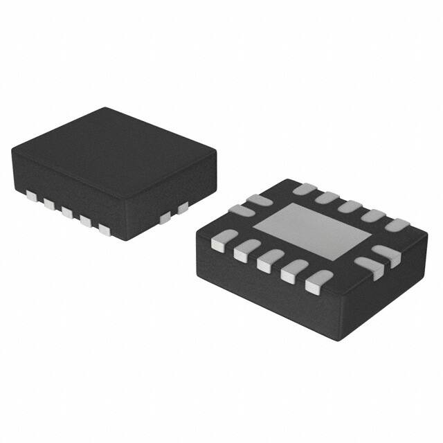
封装信息:74LV14有多种封装选项,包括SO14、SSOP14、TSSOP14和DHVQFN14。