CGH35015
15 W, 3.3-3.9 GHz, 28V, GaN HEMT for WiMAX
Description
Cree’s CGH35015 is a gallium nitride (GaN) high electron mobility
transistor designed specifically for 802.16-2004 WiMAX Fixed
Access applications. GaN HEMTs offer high efficiency, high gain
and wide bandwidth capabilities, which makes the CGH35015
ideal for 3.3-3.9 GHz WiMAX and BWA amplifier applications. The
transistor is available in both screw-down, flange and solderdown, pill packages.
Package Types: 440166 and 440196
PN’s: CGH35015F and CGH35015P
Typical Performance Over 3.3-3.8 GHz (TC = 25˚C) of Demonstration Amplifier
Parameter
3.3 GHz
3.4 GHz
3.5 GHz
3.6 GHz
3.7 GHz
3.8 GHz
Units
Small Signal Gain
13.6
12.8
12.3
12.2
12.3
12.8
dB
EVM at PAVE = 24 dBm
2.71
2.31
2.1
2.12
2.54
3.04
%
EVM at PAVE = 33 dBm
2.63
2.29
1.93
1.70
1.70
2.14
%
Drain Efficiency at PAVE = 33 dBm
24.0
25.5
26.1
25.6
23.8
2.38
%
Note: Measured in the CGH35015F-AMP amplifier circuit, under 802.16 OFDM, 3.5 MHz Channel BW, 1/4 Cyclic Prefix, 64 QAM Modulated Burst, 5 ms
Burst, Symbol Length of 59, Coding Type RS-CC, Coding Rate Type 2/3, PAR = 9.8 dB @ 0.01 % Probability on CCDF.
Features
•
•
•
•
•
3.3 - 3.9 GHz Operation
15 W Peak Power Capability
12 dB Small Signal Gain
2.0 W PAVE at < 2.0% EVM
26% Efficiency at 2 W Average Power
•
•
WiMAX Fixed Access 802.16-2004 OFDM
WiMAX Mobile Access 802.16e OFDMA
Large Signal Models Available for ADS and MWO
Rev 4.1 – April 2020
4600 Silicon Drive | Durham, NC 27703 | wolfspeed.com
�CGH35015
2
Absolute Maximum Ratings (not simultaneous) at 25˚C Case Temperature
Parameter
Symbol
Rating
Units
Conditions
Drain-Source Voltage
VDSS
120
Volts
25˚C
Gate-to-Source Voltage
VGS
-10, +2
Volts
25˚C
Power Dissipation
PDISS
7
Watts
Storage Temperature
TSTG
-65, +150
˚C
Operating Junction Temperature
TJ
225
˚C
Maximum Forward Gate Current
IGMAX
4.0
mA
25˚C
Maximum Drain Current
IDMAX
1.5
A
25˚C
Soldering Temperature2
TS
245
˚C
Screw Torque
τ
40
in-oz
Thermal Resistance, Junction to Case3
RθJC
8.0
˚C/W
Case Operating Temperature
TC
-40, +150
˚C
1
3
85˚C
Notes:
1
Current limit for long term, reliable operation
2
Refer to the Application Note on soldering at wolfspeed.com/RF/Document-Library
3
Measured for the CGH55015 at PDISS = 7 W
Electrical Characteristics (TC = 25˚C)
Characteristics
Symbol
Min.
Typ.
Max.
Units
Conditions
Gate Threshold Voltage
VGS(th)
-3.8
-3.0
-2.3
VDC
VDS = 10 V, ID = 3.6 mA
Gate Quiescent Voltage
VGS(Q)
–
-2.7
–
VDC
VDS = 28 V, ID = 60 mA
Saturated Drain Current
IDS
2.9
3.5
–
A
VDS = 6.0 V, VGS = 2.0 V
Drain-Source Breakdown Voltage
V(BR)DSS
84
–
–
VDC
VGS = -8 V, ID = 3.6 mA
DC Characteristics1
RF Characteristics2,3 (TC = 25˚C, F0 = 3.5 GHz unless otherwise noted)
Small Signal Gain
GSS
10.5
12
–
dB
VDD = 28 V, IDQ = 100 mA
Drain Efficiency
η
22
26
–
%
VDD = 28 V, IDQ = 100 mA, PAVE = 2.0 W
Back-Off Error Vector Magnitude
EVM1
–
2.5
–
%
VDD = 28 V, IDQ = 100 mA, PAVE = 18 dBm
Error Vector Magnitude
EVM2
–
2.5
–
%
VDD = 28 V, IDQ = 100 mA, PAVE = 2.0 W
Output Mismatch Stress
VSWR
–
–
10 : 1
Y
No damage at all phase angles,
VDD = 28 V, IDQ = 100 mA, PAVE = 2.0 W
Input Capacitance
CGS
–
4.5
–
pF
VDS = 28 V, Vgs = -8 V, f = 1 MHz
Output Capacitance
CDS
–
1.3
–
pF
VDS = 28 V, Vgs = -8 V, f = 1 MHz
Feedback Capacitance
CGD
–
0.2
–
pF
VDS = 28 V, Vgs = -8 V, f = 1 MHz
4
Dynamic Characteristics
Notes:
1
Measured on wafer prior to packaging
2
Measured in the CGH35015F-AMP test fixture
Rev 4.1 – April 2020
Under 802.16 OFDM, 3.5 MHz Channel BW, 1/4 Cyclic Prefix, 64 QAM
Modulated Burst, 5 ms Burst, Symbol Length of 59, Coding Type RS-CC,
Coding RateType 2/3, PAR = 9.8 dB @ 0.01 % Probability on CCDF
4
Drain Efficiency = POUT / PDC
3
4600 Silicon Drive | Durham, NC 27703 | wolfspeed.com
�CGH35015
3
Typical WiMAX Performance
Figure 1. Small Signal S-Parameters vs Frequency measured in the CGH35015F-AMP
VDD = 28 V, IDQ = 100 mA
16
6
3
12
0
10
-3
8
-6
6
-9
4
-12
S11
S21
2
S11 (dB)
14
S11 (dB)
S21 (dB)
S21 (dB)
S21
-15
S11
0
-18
2.5
2.6
2.7
2.8
2.9
3
3.1
3.2
3.3
3.4
3.5
3.6
3.7
3.8
3.9
4
4.1
4.2
4.3
4.4
Frequency (GHz)
Frequency (GHz)
Figure 2. Typical EVM and Efficiency versus Frequency measured in the CGH35015F-AMP
VDD = 28 V, IDQ = 100 mA, 802.16-2004 OFDM, PAR = 9.8 dB
EVM and Efficiency vs. Freq.
6.0
30%
5.0
25%
Drain
Efficiency
15%
EVM @
24 dBm
2.0
Efficiency
3.0
Efficiency
20%
EVM (%)
EVM (%)
4.0
10%
EVM @
33 dBm
EVM @ 24dBm
1.0
5%
EVM @ 33dBm
Eff. @ 33dBm
0.0
0%
3.3
3.4
3.4
3.5
3.5
3.6
3.6
3.7
3.7
3.8
3.8
Frequency (GHz)
Frequency (GHz)
Note: 802.16 OFDM, 3.5 MHz Channel BW, 1/4 Cyclic Prefix, 64 QAM Modulated Burst,Symbol Length of 59, Coding Type RS-CC, Coding Rate Type 2/3
Rev 4.1 – April 2020
4600 Silicon Drive | Durham, NC 27703 | wolfspeed.com
�CGH35015
4
Typical WiMAX Performance
Figure 3. Drain Efficiency and Gain vs Output Power measured in the CGH35015F-AMP
VDD = 28 V, IDQ = 100 mA, 802.16-2004 OFDM, PAR = 9.8 dB
16
32%
14
28%
24%
10
20%
8
16%
Efficiency
6
12%
4
8%
Gain
2
Drain Efficiency (dB)
12
Drain Efficiency
Gain (dB)
Gain (dB)
Gain
4%
Drain Efficiency
0
0%
16
18
20
22
24
26
28
30
32
34
Output Power (dBm)
Output Power (dBm)
Figure 4. Typical EVM and Efficiency versus Power Output measured in the CGH35015F-AMP
VDD = 28 V, IDQ = 100 mA, 802.16-2004 OFDM, PAR = 9.8 dB
5.0
30%
4.5
27%
EVM
4.0
24%
Efficiency
18%
2.5
15%
2.0
12%
1.5
9%
EVM
1.0
Efficiency
EVM (%)
EVM (%)
Efficiency
3.0
Efficiency (dB)
21%
3.5
6%
3%
0.5
0%
0.0
16
18
20
22
24
26
Output Power (dBm)
28
30
32
34
Output Power (dBm)
Note: Under 802.16 OFDM, 3.5 MHz Channel BW, 1/4 Cyclic Prefix, 64 QAM Modulated Burst, Symbol Length of 59, Coding Type RS-CC, Coding Rate Type 2/3
Rev 4.1 – April 2020
4600 Silicon Drive | Durham, NC 27703 | wolfspeed.com
�CGH35015
5
Typical Performance
K Factor
MAG (dB)
Figure 5. Simulated Maximum Available Gain and K Factor of the CGH35015
VDD = 28 V, IDQ = 100 mA
GMAX and K of CGH35015F at Idq of 100mA
Frequency (GHz)
Typical Noise Performance
Noise Resistance (Ohms)
Minimum Noise Figure (dB)
Figure 6. Simulated Minimum Noise Figure and Noise Resistance vs Frequency of the CGH35015
VDD = 28 V, IDQ = 100 mA
Frequency (GHz)
Rev 4.1 – April 2020
4600 Silicon Drive | Durham, NC 27703 | wolfspeed.com
�CGH35015
6
Source and Load Impedances
D
Z Source
Z Load
G
Frequency
Z Source
Z Load
3300
13.0 - j5.6
13.2 - j2.8
3400
17.2 - j6.0
13.2 - j2.8
3500
20.8 - j9.9
13.1 - j2.9
3600
20.1 - j15.8
13.1 - j3.3
3700
15.7 - j19.0
12.3 - j3.8
S
Note 1. VDD = 28V, IDQ = 115 mA in the 440166 package
Note 2. Impedances are extracted from the CGH35015F-AMP demonstration amplifier
and are not source and load pull data derived from the transistor
Electrostatic Discharge (ESD) Classifications
Parameter
Symbol
Class
Test Methodology
Human Body Model
HBM
1A (> 250 V)
JEDEC JESD22 A114-D
Charge Device Model
CDM
II (200 < 500 V)
JEDEC JESD22 C101-C
Rev 4.1 – April 2020
4600 Silicon Drive | Durham, NC 27703 | wolfspeed.com
�CGH35015
7
CGH35015F-AMP Demonstration Amplifier Circuit Bill of Materials
Designator
Description
Qty
C1, C2
CAP, 0.8pF, +/-0.1 pF, 0603, ATC 600S
2
C10, C11
CAP, 2.4pF,+/-0.1pF, 0603, ATC 600S
2
C4, C12
CAP, 10.0pF, +/-5%, 0603, ATC 600S
1
C5, C13
CAP, 39 PF±5%, 0603, ATC 600S
2
C14
CAP, 100 PF±5%, 0603, ATC 600S
1
C6
CAP, 470 PF ±10%,100 V, 0603
1
C7, C15
CAP, 33000PF, 100V, 0805, X7R
2
C8
CAP, 10UF, 16V, SMT, TANTALUM (240096)
1
C16
CAP, 1.0UF ±10%, 100V, 1210, X7R
1
C17
CAP, 33UF, 100V, ELECT, FK, SMD
1
R3
RES, 1/16W, 0603, 22 Ohms ≤5%
1
R4
RES, 1/16W, 0603, 100 Ohms ≤5%
1
J1
5-PIN, MOLEX, MALE, CONNECTOR
1
J2
2-PIN, MOLEX, MALE, CONNECTOR
1
J3, J4
SMA, FEMALE, CONNECTOR
2
-
PCB, RO4350B, Er = 3.48, h = 20 mil
1
-
CGH35015F or CGH35015P
1
CGH35015F-AMP Demonstration Amplifier Circuit
Rev 4.1 – April 2020
4600 Silicon Drive | Durham, NC 27703 | wolfspeed.com
�CGH35015
8
CGH35015-AMP Demonstration Amplifier Circuit Schematic
CGH35015-AMP Demonstration Amplifier Circuit Outline
Rev 4.1 – April 2020
4600 Silicon Drive | Durham, NC 27703 | wolfspeed.com
�CGH35015
9
Typical Package S-Parameters for CGH35015
(Small Signal, VDS = 28 V, IDQ = 100 mA, angle in degrees)
Frequency
Mag S11
Ang S11
Mag S21
Ang S21
Mag S12
Ang S12
Mag S22
Ang S22
500 MHz
0.909
-124.41
17.41
107.81
0.026
21.06
0.335
-93.73
600 MHz
0.902
-134.04
15.04
101.48
0.027
15.39
0.322
-101.61
700 MHz
0.898
-141.62
13.18
96.16
0.028
10.74
0.315
-107.78
800 MHz
0.894
-147.78
11.71
91.54
0.028
6.79
0.312
-112.73
900 MHz
0.892
-152.91
10.51
87.43
0.028
3.35
0.312
-116.77
1.0 GHz
0.890
-157.30
9.53
83.68
0.028
0.28
0.314
-120.15
1.1 GHz
0.889
-161.12
8.71
80.20
0.028
-2.51
0.318
-123.04
1.2 GHz
0.889
-164.51
8.01
76.95
0.028
-5.07
0.322
-125.57
1.3 GHz
0.888
-167.56
7.41
73.86
0.028
-7.45
0.328
-127.82
1.4 GHz
0.888
-170.34
6.89
70.91
0.028
-9.69
0.335
-129.87
1.5 GHz
0.888
-172.91
6.44
68.07
0.028
-11.81
0.342
-131.77
1.6 GHz
0.888
-175.30
6.04
65.32
0.028
-13.82
0.349
-133.56
1.7 GHz
0.888
-177.55
5.69
62.65
0.027
-15.74
0.357
-135.25
1.8 GHz
0.888
-179.68
5.37
60.05
0.027
-17.58
0.364
-136.89
1.9 GHz
0.888
178.29
5.09
57.50
0.027
-19.34
0.373
-138.48
2.0 GHz
0.888
176.34
4.83
55.01
0.027
-21.04
0.381
-140.03
2.1 GHz
0.889
174.45
4.60
52.56
0.026
-22.69
0.389
-141.55
2.2 GHz
0.889
172.63
4.39
50.14
0.026
-24.27
0.397
-143.06
2.3 GHz
0.889
170.84
4.20
47.76
0.026
-25.80
0.405
-144.56
2.4 GHz
0.889
169.10
4.02
45.41
0.025
-27.28
0.413
-146.04
2.5 GHz
0.890
167.39
3.86
43.09
0.025
-28.70
0.421
-147.52
2.6 GHz
0.890
165.71
3.71
40.79
0.025
-30.08
0.429
-149.00
2.7 GHz
0.891
164.04
3.57
38.51
0.024
-31.41
0.437
-150.48
2.8 GHz
0.891
162.39
3.44
36.26
0.024
-32.69
0.445
-151.95
2.9 GHz
0.891
160.76
3.32
34.01
0.024
-33.92
0.452
-153.43
3.0 GHz
0.892
159.13
3.21
31.79
0.023
-35.10
0.459
-154.92
3.2 GHz
0.892
155.89
3.00
27.38
0.023
-37.31
0.473
-157.90
3.4 GHz
0.893
152.65
2.83
23.00
0.022
-39.32
0.486
-160.90
3.6 GHz
0.893
149.39
2.67
18.66
0.021
-41.09
0.499
-163.93
3.8 GHz
0.894
146.09
2.54
14.34
0.020
-42.63
0.510
-166.99
4.0 GHz
0.894
142.74
2.41
10.02
0.020
-43.90
0.521
-170.10
4.2 GHz
0.895
139.33
2.31
5.70
0.019
-44.88
0.530
-173.24
4.4 GHz
0.895
135.84
2.21
1.37
0.018
-45.53
0.539
-176.45
4.6 GHz
0.895
132.26
2.12
-2.98
0.018
-45.84
0.547
-179.71
4.8 GHz
0.895
128.59
2.04
-7.36
0.017
-45.78
0.554
176.97
5.0 GHz
0.895
124.80
1.97
-11.79
0.016
-45.32
0.561
173.56
5.2 GHz
0.895
120.90
1.91
-16.27
0.016
-44.47
0.566
170.07
5.4 GHz
0.895
116.87
1.85
-20.81
0.016
-43.25
0.571
166.48
5.6 GHz
0.895
112.70
1.80
-25.41
0.015
-41.72
0.575
162.78
5.8 GHz
0.895
108.38
1.75
-30.10
0.015
-39.97
0.579
158.96
6.0 GHz
0.895
103.92
1.70
-34.88
0.016
-38.13
0.581
155.00
To download the s-parameters in s2p format, go to the CGH35015 Product page and click on the documentation tab.
Rev 4.1 – April 2020
4600 Silicon Drive | Durham, NC 27703 | wolfspeed.com
�CGH35015
10
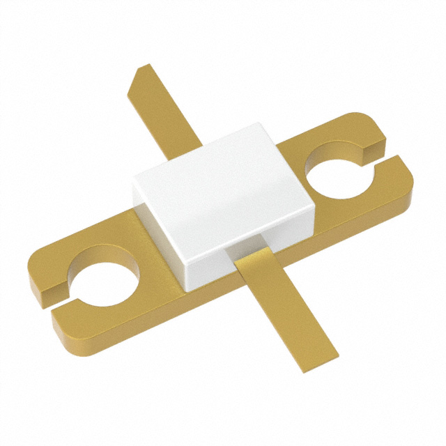
Product Dimensions CGH35015F (Package Type — 440166)
Product Dimensions CGH35015P (Package Type — 440196)
Rev 4.1 – April 2020
4600 Silicon Drive | Durham, NC 27703 | wolfspeed.com
�CGH35015
11
Product Ordering Information
Order Number
Description
Unit of Measure
CGH35015F
GaN HEMT
Each
CGH35015P
GaN HEMT
Each
CGH35015-AMP
Test board with GaN HEMT installed
Each
Rev 4.1 – April 2020
Image
4600 Silicon Drive | Durham, NC 27703 | wolfspeed.com
�CGH35015
12
For more information, please contact:
4600 Silicon Drive
Durham, North Carolina, USA 27703
www.wolfspeed.com/RF
Sales Contact
RFSales@cree.com
Notes
Disclaimer
Specifications are subject to change without notice. “Typical” parameters are the average values expected by Cree in
large quantities and are provided for information purposes only. Cree products are not warranted or authorized for use
as critical components in medical, life-saving, or life-sustaining applications, or other applications where a failure would
reasonably be expected to cause severe personal injury or death. No responsibility is assumed by Cree for any infringement of patents or other rights of third parties which may result from use of the information contained herein. No license
is granted by implication or otherwise under any patent or patent rights of Cree.
© 2005-2020 Cree, Inc. All rights reserved. Wolfspeed® and the Wolfspeed logo are registered trademarks of Cree, Inc.
Rev 4.1 – April 2020
4600 Silicon Drive | Durham, NC 27703 | wolfspeed.com
�


 工商网监
湘ICP备2023018690号
工商网监
湘ICP备2023018690号
