a
CMOS 3 V/5 V, Wide Bandwidth Quad 2:1
Mux in Chip Scale Package
ADG784
FEATURES
Low Insertion Loss and On Resistance: 4 � Typical
On-Resistance Flatness 200 MHz
Single 3 V/5 V Supply Operation
Rail-to-Rail Operation
Very Low Distortion: 200 MHz.
3. Ultralow Power Dissipation.
4. Extended Signal Range.
The ADG784 is fabricated on a CMOS process giving an
increased signal range that fully extends to the supply rails.
5. Low Leakage over Temperature.
6. Break-Before-Make Switching.
This prevents channel shorting when the switches are configured as a multiplexer.
7. Crosstalk is typically –70 dB @ 30 MHz.
8. Off isolation is typically –60 dB @ 10 MHz.
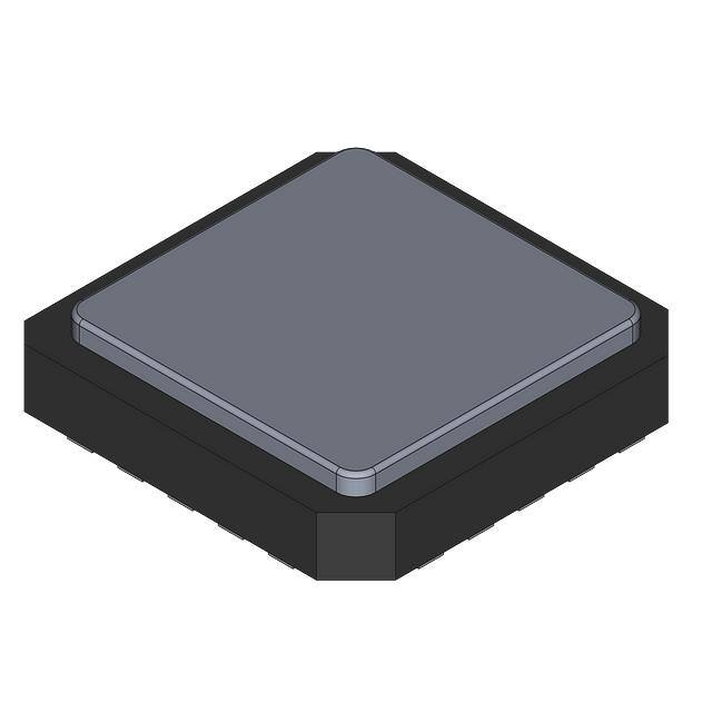
9. Available in Chip Scale Package (CSP).
REV. 0
Information furnished by Analog Devices is believed to be accurate and
reliable. However, no responsibility is assumed by Analog Devices for its
use, nor for any infringements of patents or other rights of third parties that
may result from its use. No license is granted by implication or otherwise
under any patent or patent rights of Analog Devices.
One Technology Way, P.O. Box 9106, Norwood, MA 02062-9106, U.S.A.
Tel: 781/329-4700
www.analog.com
Fax: 781/326-8703
© Analog Devices, Inc., 2001
�ADG784–SPECIFICATIONS
SINGLE SUPPLY (V
DD
= 5 V � 10%, GND = 0 V. All specifications TMIN to TMAX unless otherwise noted.)
Parameter
B Version
TMIN to
25�C
TMAX
ANALOG SWITCH
Analog Signal Range
On Resistance (RON)
2.2
0 V to VDD
5
On Resistance Match Between
Channels (∆RON)
0.15
0.5
On Resistance Flatness (RFLAT(ON))
0.5
1
LEAKAGE CURRENTS
Source OFF Leakage IS (OFF)
Drain OFF Leakage ID (OFF)
Channel ON Leakage ID, IS (ON)
DIGITAL INPUTS
Input High Voltage, VINH
Input Low Voltage, VINL
Input Current
IINL or IINH
± 0.01
± 0.5
± 0.01
± 0.5
± 0.01
± 0.5
tOFF
Break-Before-Make Time Delay, tD
Off Isolation
Channel-to-Channel Crosstalk
Bandwidth –3 dB
Distortion
Charge Injection
CS (OFF)
CD (OFF)
CD, CS (ON)
Test Conditions/Comments
V
Ω typ
Ω max
VD = 0 V to VDD, IS = –10 mA
Ω typ
Ω max
Ω typ
Ω max
2.4
0.8
V min
V max
± 0.5
µA typ
µA max
VIN = VINL or VINH
10
20
4
8
5
1
–65
–75
240
0.5
10
10
20
30
ns typ
ns max
ns typ
ns max
ns typ
ns min
dB typ
dB typ
MHz typ
% typ
pC typ
pF typ
pF typ
pF typ
RL = 100 Ω, CL = 35 pF,
VS = 3 V; Test Circuit 4
RL = 100 Ω, CL = 35 pF,
VS = 3 V; Test Circuit 4
RL = 100 Ω, CL = 35 pF,
VS1 = VS2 = 5 V; Test Circuit 5
RL = 100 Ω, f = 10 MHz; Test Circuit 7
RL = 100 Ω, f = 10 MHz; Test Circuit 8
RL = 100 Ω; Test Circuit 6
RL = 100 Ω
CL = 1 nF; Test Circuit 9
f = 1 kHz
f = 1 kHz
f = 1 MHz
1
0.001
IIN
IO
VD = 0 V to VDD; IS = –10 mA
±1
±1
POWER REQUIREMENTS
IDD
VD = 0 V to VDD, IS = –10 mA
nA typ
nA max
nA typ
nA max
nA typ
nA max
±1
0.001
DYNAMIC CHARACTERISTICS2
tON
Unit
1
100
µA max
µA typ
µA typ
mA max
VD = 4.5 V, VS = 1 V; VD = 1 V, VS = 4.5 V;
Test Circuit 2
VD = 4.5 V, VS = 1 V; VD = 1 V, VS = 4.5 V;
Test Circuit 2
VD = VS = 4.5 V; VD = VS = 1 V; Test Circuit 3
VDD = 5.5 V
Digital Inputs = 0 V or VDD
VIN = 5 V
VS/VD = 0 V
NOTES
1
Temperature ranges are as follows: B Version, –40°C to +85°C.
2
Guaranteed by design, not subject to production test.
Specifications subject to change without notice.
–2–
REV. 0
�ADG784
SINGLE SUPPLY
(VDD = 3 V � 10%, GND = 0 V. All specifications TMIN to TMAX unless otherwise noted.)
Parameter
B Version
TMIN to
25�C
TMAX
ANALOG SWITCH
Analog Signal Range
On Resistance (RON)
4
0 V to VDD
10
On Resistance Match Between
Channels (∆RON)
±1
VD = 3 V, VS = 1 V; VD = 1 V, VS = 3 V;
Test Circuit 2
VD = 3 V, VS = 1 V; VD = 1 V, VS = 3 V;
Test Circuit 2
VD = VS = 3 V; VD = VS = 1 V; Test Circuit 3
2.0
0.4
V min
V max
± 0.5
µA typ
µA max
VIN = VINL or VINH
12
25
5
10
5
1
–65
–75
240
2
3
10
20
30
ns typ
ns max
ns typ
ns max
ns typ
ns min
dB typ
dB typ
MHz typ
% typ
pC typ
pF typ
pF typ
pF typ
RL = 100 Ω, CL = 35 pF,
VS = 1.5 V; Test Circuit 4
RL = 100 Ω, CL = 35 pF,
VS = 1.5 V; Test Circuit 4
RL = 100 Ω, CL = 35 pF,
VS1 = VS2 = 3 V; Test Circuit 5
RL = 50 Ω, f = 10 MHz; Test Circuit 7
RL = 50 Ω, f = 10 MHz; Test Circuit 8
RL = 50 Ω; Test Circuit 6
RL = 50 Ω
CL = 1 nF; Test Circuit 9
f = 1 kHz
f = 1 kHz
f = 1 MHz
4
Drain OFF Leakage ID (OFF)
Channel ON Leakage ID, IS (ON)
DIGITAL INPUTS
Input High Voltage, VINH
Input Low Voltage, VINL
Input Current
IINL or IINH
±1
±1
0.001
DYNAMIC CHARACTERISTICS2
tON
tOFF
Break-Before-Make Time Delay, tD
Off Isolation
Channel-to-Channel Crosstalk
Bandwidth –3 dB
Distortion
Charge Injection
CS (OFF)
CD (OFF)
CD, CS (ON)
VD = 0 V to VDD, IS = –10 mA
nA typ
nA max
nA typ
nA max
nA typ
nA max
2
± 0.01
± 0.5
± 0.01
± 0.5
± 0.01
± 0.5
V
Ω typ
Ω max
VD = 0 V to VDD, IS = –10 mA
0.5
LEAKAGE CURRENTS
Source OFF Leakage IS (OFF)
Test Conditions/Comments
Ω typ
Ω max
Ω typ
Ω max
0.15
On Resistance Flatness (RFLAT(ON))
Unit
VD = 0 V to VDD, IS = –10 mA
POWER REQUIREMENTS
IDD
µA max
µA typ
µA typ
mA max
1
0.001
IIN
IO
1
100
VDD = 3.3 V
Digital Inputs = 0 V or VDD
VIN = 3 V
VS/VD = 0 V
NOTES
1
Temperature ranges are as follows: B Version, –40°C to +85°C.
2
Guaranteed by design, not subject to production test.
Specifications subject to change without notice.
Table I. Truth Table
REV. 0
EN
IN
D1
D2
D3
D4
Function
1
0
0
X
0
1
Hi-Z
S1A
S1B
Hi-Z
S2A
S2B
Hi-Z
S3A
S3B
Hi-Z
S4A
S4B
DISABLE
IN = 0
IN = 1
–3–
�ADG784
ABSOLUTE MAXIMUM RATINGS 1
TERMINOLOGY
(TA = 25°C unless otherwise noted.)
VDD
GND
S
D
IN
EN
RON
∆RON
Most Positive Power Supply Potential.
Ground (0 V) Reference.
Source Terminal. May be an input or output.
Drain Terminal. May be an input or output.
Logic Control Input.
Logic Control Input.
Ohmic resistance between D and S.
On Resistance match between any two channels
i.e., RON max – RON min.
RFLAT(ON)
Flatness is defined as the difference between
the maximum and minimum value of on resistance as measured over the specified analog
signal range.
Source Leakage Current with the switch “OFF.”
IS (OFF)
ID (OFF)
Drain Leakage Current with the switch “OFF.”
ID, IS (ON) Channel Leakage Current with the switch “ON.”
VD (VS)
Analog Voltage on Terminals D, S.
CS (OFF)
“OFF” Switch Source Capacitance.
CD (OFF)
“OFF” Switch Drain Capacitance.
CD, CS (ON) “ON” Switch Capacitance.
tON
Delay between applying the digital control input
and the output switching on. See Test Circuit 4.
tOFF
Delay between applying the digital control input
and the output switching Off.
tD
“OFF” time or “ON” time measured between
the 90% points of both switches, when switching
from one address state to another. See Test
Circuit 5.
Crosstalk
A measure of unwanted signal that is coupled
through from one channel to another as a result
of parasitic capacitance.
Off Isolation A measure of unwanted signal coupling through an
“OFF” switch.
Bandwidth Frequency response of the switch in the ON
state measured at 3 dB down.
Distortion
RFLAT(ON)/RL
VDD to GND . . . . . . . . . . . . . . . . . . . . . . . . . . –0.3 V to +6 V
Analog, Digital Inputs2 . . . . . . . . . . –0.3 V to VDD + 0.3 V or
30 mA, Whichever Occurs First
Continuous Current, S or D . . . . . . . . . . . . . . . . . . . . 100 mA
Peak Current, S or D . . . . . . . . . . . . . . . . . . . . . . . . . . 300 mA
(Pulsed at 1 ms, 10% Duty Cycle max)
Operating Temperature Range
Industrial (B Version) . . . . . . . . . . . . . . . . –40°C to +85°C
Storage Temperature Range . . . . . . . . . . . . –65°C to +150°C
Junction Temperature . . . . . . . . . . . . . . . . . . . . . . . . . . 150°C
Chip Scale Package
θJA Thermal Impedance . . . . . . . . . . . . . . . . . . . . . . 32°C/W
Lead Temperature, Soldering
Vapor Phase (60 sec) . . . . . . . . . . . . . . . . . . . . . . . . . 215°C
Infrared (15 sec) . . . . . . . . . . . . . . . . . . . . . . . . . . . . . 220°C
ESD . . . . . . . . . . . . . . . . . . . . . . . . . . . . . . . . . . . . . . . . . 2 kV
NOTES
1
Stresses above those listed under Absolute Maximum Ratings may cause permanent damage to the device. This is a stress rating only; functional operation of the
device at these or any other conditions above those listed in the operational
sections of this specification is not implied. Exposure to absolute maximum rating
conditions for extended periods may affect device reliability. Only one absolute
maximum rating may be applied at any one time.
2
Overvoltages at IN, S or D will be clamped by internal diodes. Current should be
limited to the maximum ratings given.
20
19
18
17
16
IN
NC
VDD
NC
EN
PIN CONFIGURATION
1
2
3
4
5
NC = NO CONNECT
PIN 1
INDICATOR
ADG784
TOP VIEW
15
14
13
12
11
S4A
S4B
D4
S3A
S3B
D2 6
NC 7
GND 8
NC 9
D3 10
S1A
S1B
D1
S2A
S2B
NOTE: EXPOSED PAD TIED TO SUBSTRATE, GND.
ORDERING GUIDE
Model
Temperature Range
Package Description
Package Option
ADG784BCP
–40°C to +85°C
Chip Scale Package
CP-20
CAUTION
ESD (electrostatic discharge) sensitive device. Electrostatic charges as high as 4000 V readily
accumulate on the human body and test equipment and can discharge without detection. Although
the ADG784 features proprietary ESD protection circuitry, permanent damage may occur on
devices subjected to high-energy electrostatic discharges. Therefore, proper ESD precautions are
recommended to avoid performance degradation or loss of functionality.
–4–
WARNING!
ESD SENSITIVE DEVICE
REV. 0
�Typical Performance Characteristics–ADG784
5.0
0
TA = 25�C
4.5
VDD = 2.7V
VDD = 5V
4.0
3.0
ON RESPONSE – dB
RON – �
3.5
VDD = 3.0V
2.5
VDD = 4.5V
2.0
1.5
–2
–4
VDD = 5.0V
1.0
0.5
0
1.3
2.5
3.7
VS OR VD DRAIN OR SOURCE VOLTAGE – V
–6
10k
4.9
100k
10M
1M
FREQUENCY – Hz
100M
TPC 4. On Response vs. Frequency
TPC 1. On Resistance as a Function of VD (VS) for
Various Single Supplies
3.0
0
VDD = 5V
VDD = 5V
RL = 100�
–10
2.5
–20
RON – �
2.0
1.5
ATTENUATION – dB
+85�C
+25�C
–40�C
1.0
–30
–40
–50
–60
–70
–80
0.5
–90
0
1.3
2.5
3.7
VS OR VO DRAIN OR SOURCE VOLTAGE – V
–100
100k
4.9
4.5
–10
+85�C
–20
RON – �
ATTENUATION – dB
3.5
+25�C
2.5
–40�C
2.0
1.5
1.0
VDD = 5V
RL = 100�
V P-P = 0.316V
–30
–40
–50
–60
–70
–90
–100
100k
0.6
1.1
1.6
2.1
2.6
VS OR VD DRAIN OR SOURCE VOLTAGE – V
TPC 3. On Resistance as a Function of VD (VS) for
Different Temperatures with 3 V Single Supplies
REV. 0
1G
–80
0.5
0
100M
0
VDD = 3V
3.0
10M
FREQUENCY – Hz
TPC 5. Off Isolation vs. Frequency
TPC 2. On Resistance as a Function of VD (VS) for
Different Temperatures with 5 V Single Supplies
4.0
1M
1M
10M
FREQUENCY – Hz
100M
TPC 6. Crosstalk vs. Frequency
–5–
1G
�ADG784
20
VDD = 5V
TA = 25 C
CHARGE INJECTION – pC
15
10
5
0
–5
–10
0
0.5
1.0
1.5
3.0
3.5
2.0
2.5
SOURCE VOLTAGE – V
4.0
4.5
5.0
TPC 7. Charge Injection vs. Source Voltage
10 BASE TX+
TX1
10 BASE TX–
ADG784
100 BASE TX+
TX2
100 BASE TX–
RJ45
10 BASE TX+
RX1
10 BASE TX–
TRANSFORMER
100 BASE TX+
RX2
100 BASE TX–
10 BASE TX
100 BASE TX
Figure 1. Full Duplex Transceiver
TX1
120�
100�
RX1
Figure 2. Loop Back
Figure 3. Line Termination
–6–
Figure 4. Line Clamp
REV. 0
�ADG784
Test Circuits
IDS
V1
IS (OFF)
S
VS
A
D
ID (OFF)
S
D
VS
RON = V1/IDS
Test Circuit 1. On Resistance
ID (ON)
S
A
VD
D
A
VD
VS
Test Circuit 2. Off Leakage
Test Circuit 3. On Leakage
5V
0.1�F
VIN
3V
VDD
50%
S
50%
VOUT
D
90%
VS
RL
100�
IN
CL
35pF
90%
VOUT
t OFF
t ON
EN
GND
Test Circuit 4. Switching Times
5V
0.1�F
VDD
3V
S1A
VOUT
D1
VS
VIN
RL
100�
VS
CL
35pF
50%
50%
0V
S1B
VOUT
50%
50%
VS
DECODER
tD
EN
tD
GND
Test Circuit 5. Break-Before-Make Time Delay
VDD
VDD
0.1�F
0.1�F
ADG784
ADG784
NETWORK
ANALYZER
S1A
NETWORK
ANALYZER
S1A
50�
50�
VS
IN
VIN
VS
IN
VOUT
D1
VIN
50�
EN
GND
Test Circuit 6. Bandwidth
REV. 0
VOUT
D1
50�
EN
50�
GND
Test Circuit 7. Off Isolation
–7–
�ADG784
VDD
0.1�F
NETWORK
ANALYZER
ADG784
50�
S2A
C02374–2.5–4/01(0)
VS
S1A
VOUT
50�
IN
D1
VIN
D2
EN
50�
GND
Test Circuit 8. Channel-to-Channel Crosstalk
5V
VDD
VS
ADG784
S1A
D1 VOUT
CL
1nF
S1B
S2A
D2 VOUT
CL
1nF
S2B
S3A
QINJ = CL � �VOUT
D4 VOUT
CL
1nF
S4B
�VOUT
VOUT
D3 VOUT
CL
1nF
S3B
S4A
3V
VIN
1-OF-2
DECODER
EN
IN
Test Circuit 9. Charge Injection
OUTLINE DIMENSIONS
Dimensions shown in inches and (mm).
20-Lead CSP
(CP-20)
0.024 (0.60)
0.017 (0.42)
0.009 (0.24)
0.024 (0.60)
0.017 (0.42)
16
0.009 (0.24)
15
0.157 (4.0)
BSC SQ
PIN 1
INDICATOR
TOP
VIEW
0.148 (3.75)
BSC SQ
0.031 (0.80) MAX
0.026 (0.65) NOM
12� MAX
0.035 (0.90) MAX
0.033 (0.85) NOM
SEATING
PLANE
0.020 (0.50)
BSC
0.008 (0.20)
REF
0.012 (0.30)
0.009 (0.23)
0.007 (0.18)
0.030 (0.75)
0.022 (0.60)
0.014 (0.50)
0.010 (0.25)
MIN
20
1
0.080 (2.25)
0.083 (2.10) SQ
0.077 (1.95)
BOTTOM
VIEW
11
10
PRINTED IN U.S.A.
RS
6
5
0.080 (2.00)
REF
0.002 (0.05)
0.0004 (0.01)
0.0 (0.0)
CONTROLLING DIMENSIONS ARE IN MILLIMETERS
–8–
REV. 0
�


 工商网监
湘ICP备2023018690号
工商网监
湘ICP备2023018690号
