ONET8501V
www.ti.com
SLLS837B – JUNE 2007 – REVISED SEPTEMBER 2007
11.3 Gbps Differential VCSEL Driver With Output Waveform Shaping
FEATURES
1
•
•
•
•
•
•
•
•
•
•
•
Up to 11.3 Gbps Operation
2-Wire Digital Interface
Digitally Selectable Modulation Current up to
24 mApp Differential
Digitally Selectable Bias Current up to 20 mA
Automatic Power Control (APC) Loop
Supports Transceiver Management System
(TMS)
Programmable Input Equalizer
Output Waveform Control
Includes Laser Safety Features
Analog Temperature Sensor Output
Selectable Monitor Photodiode Current Range
•
•
•
•
Output Polarity Select
Single 3.3V Supply
Operating Temperature –40°C to 85°C
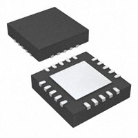
Surface Mount Small Footprint 4mm × 4mm 20
Pin RoHS compliant QFN Package
APPLICATIONS
•
•
•
•
•
10 Gigabit Ethernet Optical Transmitters
8x and 10x Fibre Channel Optical Transmitters
SONET OC-192/SDH STM-64 Optical
Transmitters
SFP+ and XFP Transceiver Modules
XENPAK, XPAK, X2 and 300-pin MSA
Transponder Modules
DESCRIPTION
The ONET8501V is a high-speed, 3.3V laser driver designed to directly modulate VCSELs at data rates from
2 Gbps up to 11.3 Gbps.
The device provides a two-wire serial interface which allows digital control of the modulation and bias currents,
eliminating the need for external components. Output waveform control, in the form of cross point control and
independent over- and undershoot capability on the rising and falling edges is also available to improve VCSEL
edge speeds and the optical eye diagram. An optional input equalizer can be used for equalization of up to
300mm (12 inch) of microstrip or stripline transmission line on FR4 printed circuit boards.
The ONET8501V includes an integrated automatic power control (APC) loop as well as circuitry to support laser
safety and transceiver management systems. The VCSEL driver is characterized for operation from –40°C to
85°C ambient temperatures and is available in a small footprint 4mm × 4mm 20 pin RoHS compliant QFN
package.
1
Please be aware that an important notice concerning availability, standard warranty, and use in critical applications of
Texas Instruments semiconductor products and disclaimers thereto appears at the end of this data sheet.
PRODUCTION DATA information is current as of publication date.
Products conform to specifications per the terms of the Texas
Instruments standard warranty. Production processing does not
necessarily include testing of all parameters.
Copyright © 2007, Texas Instruments Incorporated
�ONET8501V
www.ti.com
SLLS837B – JUNE 2007 – REVISED SEPTEMBER 2007
These devices have limited built-in ESD protection. The leads should be shorted together or the device placed in conductive foam
during storage or handling to prevent electrostatic damage to the MOS gates.
BLOCK DIAGRAM
A simplified block diagram of the ONET8501V is shown in Figure 1.
The VCSEL driver consists of an equalizer, a limiter, a waveform shaping block with over- and undershoot
control, an output driver, power-on reset circuitry, a 2-wire serial interface including a control logic block, a
modulation current generator and a bias current generator with automatic power control loop, and an analog
reference block.
Cp Adjust
DC Offset Cancellation
VCC
Equalizer
Over- / Undershoot
Generation
Delay
Buffer
+
DIN+
Output Driver
50 W 50 W
Main Driver
MOD+
+
100 W
+
+
DIN-
Limiter
Boost
Shape Control
MOD-
Peak Driver
Adjustable
Boost
SDA
SDA
8 Bit Register
4 Bit
SCK
DIS
SCK
4 Bit
DIS
4 Bit
4 Bit
7 Bit + Sign
8 Bit Register
8 Bit Register
8 Bit Register
4 Bit + Sign
4 Bit + Sign
Equalizer
OS Width
US Width
OS Height
US Height
CP Adjust
IMOD
IBIAS
Settings
TS Shift
TS Slope
2-Wire Interface & Control Logic
BIAS
MONB
Bias
Current MONP
Generator FLT
& APC
PD
COMP
Cp Adjust
RZTC
Band-Gap &
Analog References BGV
Power-On
Reset
Temperature
Sensor
TS
BIAS
MONB
MONP
FLT
PD
COMP
RZTC
BGV
TS
Figure 1. Simplified Block Diagram of the ONET8501V
2
Submit Documentation Feedback
Copyright © 2007, Texas Instruments Incorporated
Product Folder Link(s): ONET8501V
�ONET8501V
www.ti.com
SLLS837B – JUNE 2007 – REVISED SEPTEMBER 2007
PACKAGE
The ONET8501V is packaged in a small footprint 4mm × 4mm 20 pin RoHS compliant QFN package with a lead
pitch of 0,5 mm. The pin out is shown below.
VCC
MOD+
MOD-
VCC
BIAS
20 PIN QFN PACKAGE
4 mm × 4 mm (TOP VIEW)
20
19
18
17
16
15 PD
DIS 1
RZTC 2
14 COMP
ONET
8501V
20 Pin QFN
TS 3
13 MONP
6
7
8
9
10
GND
FLT
11 BGV
DIN-
SDA 5
DIN+
12 MONB
GND
SCK 4
TERMINAL FUNCTIONS
TERMINAL
PIN
NO.
NAME
TYPE
DESCRIPTION
1
DIS
Digital-in
Disables bias, modulation and peaking currents when set to high state. Toggle to reset a fault condition.
Recommend shorting pin to GND if disable feature is not used.
2
RZTC
Analog
Connect external zero TC 28.7kΩ resistor to ground (GND). Used to generate a defined zero TC
reference current for internal DACs.
3
TS
Analog-out
Temperature sensor output.
4
SCK
Digital -in
2-wire interface serial clock. Includes a pull-up resistor to VCC.
5
SDA
Digital -in
2-wire interface serial data input. Includes a pull-up resistor to VCC.
6, 9, EP GND
Supply
Circuit ground. Exposed die pad (EP) must be grounded.
7
DIN+
Analog-in
Non-inverted data input. On-chip differentially 100Ω terminated to DIN–. Must be AC coupled.
8
DIN–
Analog-in
Inverted data input. On-chip differentially 100Ω terminated to DIN+. Must be AC coupled.
10
FLT
Digital-out
Fault detection flag. LVCMOS output with source and sink capability.
11
BGV
Anolog-out
Buffered bandgap voltage with 1.16V output. This is a replica of the bandgap voltage at RZTC. For best
matching, use the same 28.7kΩ resistor to GND as used at RZTC.
12
MONB
13
MONP
14
COMP
15
PD
16
BIAS
17, 20
VCC
Analog-out
Bias current monitor. Sources a 3.5% replica of the bias current. Connect an external resistor to ground
(GND). If the voltage at this pin exceeds 1.16V a fault is triggered. Typically choose a resistor to give
MONB voltage of 0.8V at the maximum desired bias current.
Photodiode current monitor. Sources a 27% replica of the photodiode current when PDR = 10, a 54%
replica when PDR = 01, and a 270% replica when PDR=00. Connect an external resistor (5kΩ typical) to
ground (GND).
Compensation pin used to control the bandwidth of the APC loop. Connect a 0.01μF capacitor to ground.
Analog
Photodiode input. Pin can source or sink current dependent on register setting.
Sinks average bias current for VCSEL in both APC and open loop modes. Connect to laser cathode
through an inductor. BLM15HG102SN1D recommended.
Supply
3.3V ± 10% supply voltage
Submit Documentation Feedback
Copyright © 2007, Texas Instruments Incorporated
Product Folder Link(s): ONET8501V
3
�ONET8501V
www.ti.com
SLLS837B – JUNE 2007 – REVISED SEPTEMBER 2007
TERMINAL FUNCTIONS (continued)
TERMINAL
PIN
NO.
NAME
18
MOD–
19
MOD+
TYPE
DESCRIPTION
Inverted modulation current output. On-chip 50Ω back-terminated to VCC. IMOD flows into this pin when
input data is low.
CML-out
(current)
Non-inverted modulation current output. On-chip 50Ω back-terminated to VCC. IMOD flows into this pin
when input data is high.
ABSOLUTE MAXIMUM RATINGS (1)
over operating free-air temperature range (unless otherwise noted)
VALUE
UNIT
VCC
Supply voltage (2)
–0.3 to 4
V
VDIS, VRZTC, VTS, VSCK,
VSDA, VFLT, VBGV, VMONB,
VMONP, VCAPC, VPD, VBIAS
VDIN+, VDIN–, VMOD+, VMOD–
Voltage at DIS, RZTC, TS, SCK, SDA, FLT, BGV, MONB, MONP, CAPC,
PD, BIAS, DIN+, DIN–, MOD+, MOD– (2)
–0.3 to 4
V
IDIN–, IDIN+
Maximum current at input pins
25
mA
IMOD+, IMOD–
Maximum current at output pins
30
mA
ESD
ESD rating at all pins
2
kV (HBM)
TJ,max
Maximum junction temperature
125
°C
TSTG
Storage temperature range
–65 to 150
°C
TA
Characterized free-air operating temperature range
–40 to 85
°C
(1)
(2)
Stresses beyond those listed under absolute maximum ratings may cause permanent damage to the device. These are stress ratings
only, and functional operation of the device at these or any other conditions beyond those indicated under recommended operating
conditions is not implied. Exposure to absolute-maximum-rated conditions for extended periods may affect device reliability
All voltage values are with respect to network ground terminal
RECOMMENDED OPERATING CONDITIONS
over operating free-air temperature range (unless otherwise noted)
MIN
VCC
Supply voltage
VIH
Digital input high voltage
DIS, SCK, SDA
VIL
Digital input low voltage
DIS, SCK, SDA
Bias output headroom voltage
VBIAS – GND
Photodiode current range
2.95
TYP MAX
3.3
3.6
2
UNIT
V
V
0.8
300
V
mV
High step size mode, min. step size = 5 μA
25
High step size mode, max. step size = 5 μA
1280
Medium step size mode, min. step size = 2.5 μA
12.5
Medium step size mode, max. step size = 2.5 μA
640
Low step size mode, min. step size = 0.5 μA
2.5
Low step size mode, max. step size = 0.5 μA
128
μA
RRZTC
Zero TC resistor value (1)
vIN
Differential input voltage swing
tR-IN
Input rise time
20%–80%
30
55
ps
tF-IN
Input fall time
20%–80%
30
55
ps
TA
Operating free-air temperature
85
°C
(1)
4
1.16 V bandgap bias across resistor, E96, 1% accuracy
28.4
28.7
100
–40
29
1200
kΩ
mVpp
Changing the value will alter the DAC ranges.
Submit Documentation Feedback
Copyright © 2007, Texas Instruments Incorporated
Product Folder Link(s): ONET8501V
�ONET8501V
www.ti.com
SLLS837B – JUNE 2007 – REVISED SEPTEMBER 2007
DC ELECTRICAL CHARACTERISTICS
Over recommended operating conditions, all values are for open-loop operation, IMODC = 12 mA, IBIASC = 6 mA, and
RRZTC = 28.7 kΩ, unless otherwise noted
PARAMETER
VCC
TEST CONDITIONS
MIN
TYP
MAX
2.95
3.3
3.6
IMODC = 12 mA, IBIASC = 6 mA, including IMODC, No waveform
shaping, EQENA = 0
50
70
IMODC = 12 mA, IBIASC = 6 mA, including IMODC, No waveform
shaping, EQENA = 1
55
75
IMODC = 12 mA, IBIASC = 6 mA, including IMODC, Single sided max
output waveform shaping at MOD+ or MOD–, EQENA = 1
75
90
IMODC = 12 mA, IBIASC = 6 mA, including IMODC, Double sided max
output waveform shaping at MOD+ or MOD–, EQENA = 1
82
100
Supply voltage
IVCC
Supply current
Disabled (DIS=HIGH) or ENA=LOW, EQENA = 0
UNIT
V
mA
24
Ω
RIN
Data input resistance
Differential between DIN+ / DIN–
80
100
120
ROUT
Data output resistance
Single-ended to VCC
40
50
60
Ω
Digital input current
SCK, SDA, pull up to VCC (1)
–10
10
μA
Digital input current
DIS, pull down to GND (1)
–10
10
μA
VOH
Digital output high voltage
FLT, pull-up to VCC, ISOURCE = 1000 μA (2)
2.4
VOL
Digital output low voltage
FLT, pull-up to VCC, ISINK = 1000 μA (2)
IBIAS-DIS
Bias current during disable
IBIAS-MIN
Minimum bias current
See
IBIAS-MAX
Maximum bias current
DAC set to maximum, open and closed loop
17
VPD
Photodiode reverse bias voltage
APC active, IPD = max
1.3
Photodiode fault current level
Percent of target IPD (1)
(3)
ITS
μA
20
mA
2.3
V
0.5
(1)
With mid scale calibration
Temperature sensor drive current
Source or sink (1)
2.5
±4
°C
μA
20%
27%
IMONP / IPD with control bit PDR = 01
40%
54%
65%
IMONP / IPD with control bit PDR = 00
200%
270%
350%
2.9%
3.5%
4.2%
2.4
2.5
2.8
Bias current monitor ratio
IMONB / IBIAS (nominal 1/30 = 3.3%) 1.2 kΩ sense resistor.
VCC reset threshold voltage
VCC voltage level which triggers power-on reset
VCC-RSTHYS
VCC reset threshold voltage
hysteresis
VMONB-FLT
Fault voltage at MONB
32%
100
Fault occurs if voltage at MONB exceeds value
1.1
V
100
IMONP / IPD with control bit PDR = 10
VCC-RST
(1)
(2)
(3)
μA
150%
Temperature sensor accuracy
Photodiode current monitor ratio
V
100
200
Temperature sensor voltage range –40°C to 120°C junction temperature. With Mid scale calibration(1)
VTS
V
0.4
1.16
V
mV
1.2
V
Specified by simulation over process, supply and temperature variation
External pull up resistor according to timing requirements
The bias current can be set below the specified minimum according to the corresponding register setting, however in closed loop
operation settings below the specified value may trigger a fault.
Submit Documentation Feedback
Copyright © 2007, Texas Instruments Incorporated
Product Folder Link(s): ONET8501V
5
�ONET8501V
www.ti.com
SLLS837B – JUNE 2007 – REVISED SEPTEMBER 2007
AC ELECTRICAL CHARACTERISTICS
Over recommended operating conditions with 50Ω output load, open loop operation, IMODC = 12 mA, IBIAS = 6 mA, and
RRZTC = 28.7 kΩ, unless otherwise noted. Typical operating condition is at VCC = 3.3V and TA = 25°C
PARAMETER
TEST CONDITIONS
MIN
0.01 GHz < f < 3.9 GHz
SDD11
SCD11
tR-OUT
Differential input return gain
Differential to common mode
conversion gain
Output rise time
3.9 GHz < f < 11.1 GHz
(1)
11.1 GHz < f < 20 GHz
–3
f < 8.25 GHz
–35
8.25 GHz < f < 20 GHz
–28
20% – 80%, tR-IN < 40 ps, 100 Ω differential load, no waveform
shaping, EQENA = 0, 100 mVpp differential input voltage
20% – 80%, tF-IN < 40 ps, 100 Ω differential load, no waveform
shaping, EQENA = 0, 100 mVpp differential input voltage
IMOD-MAX
Maximum modulation current
Output stage tail current
IMOD-STEP
Modulation current step size full
Modulation current step size half
DJ
Deterministic output jitter
Maximum output peaking width
Minimum output peaking width
Maximum output peaking height
Output peaking height step size
16
dB
30
24
30
24
ps
mA
100
μA
Modulation current smaller than 6 mA
50
EQENA = 0, K28.5 pattern at 11.3 Gbps, no waveform shaping,
100 mVpp, 600 mVpp, 1200 mVpp differential input voltage
3.5
9
8.5
15
psp-p
EQENA = 1, K28.5 pattern at 11.3 Gbps, maximum equalization
with 12” transmission line at the input, no waveform shaping,
200 mVpp, 600 mVpp, 1200 mVpp differential input voltage
120
Maximum peaking height (2)
ps
30
Referred to output stage tail current, high range
10
Referred to output stage tail current, low range
5
Referred to output stage tail current, high range
0.66
Referred to output stage tail current, low range
0.33
Cross point range
600 mVpp differential input
Random output jitter
50Ω load, EQENA = 0, 100 mVpp differential input voltage
0.4
τAPC
APC time constant
CAPC 0.01 μF, IPD = 100 μA, PD coupling ratio CR = 40 (2)
200
tOFF
Transmitter disable time
Rising edge of DIS to IBIAS ≤ 0.1× IBIAS-NOMINAL (2)
tON
Disable negate time
Falling edge of DIS to IBIAS ≥ 0.9 × IBIAS-NOMINAL
tINIT1
Power-on to initialize
Power-on to registers ready to be loaded
tINIT2
Initialize to transmit
Register load STOP command to part ready to transmit valid data (2)
tRESET
DIS pulse width
Time DIS must held high to reset part (2)
tFAULT
Fault assert time
Time from fault condition to FLT high (2)
6
UNIT
dB
24
RJ
(1)
(2)
MAX
–16
Output fall time
tF-OUT
TYP
mA
mA
30–70%
1
(2)
0.2
0.6
psRMS
μs
5
μs
1
ms
1
ms
2
ms
50
μs
100
ns
Differential Return Gain given by SDD11 = –14 + 13.33 log10(f/5.5), f in GHz
Assured by simulation over process, supply and temperature variation
Submit Documentation Feedback
Copyright © 2007, Texas Instruments Incorporated
Product Folder Link(s): ONET8501V
�ONET8501V
www.ti.com
SLLS837B – JUNE 2007 – REVISED SEPTEMBER 2007
DETAILED DESCRIPTION
EQUALIZER
The data signal can be applied to an input equalizer by means of the input signal pins DIN+/DIN–, which provide
on-chip differential 100Ω line-termination. The equalizer is enabled by setting the EQENA = 1 (bit 1 of register 0).
Equalization of up to 300mm (12”) of microstrip or stripline transmission line on FR4 printed circuit boards can be
achieved. The amount of equalization is digitally controlled by the two-wire interface and control logic block and
depends on the register settings EQADJ[0..7] (register 3). The equalizer can also be turned off and bypassed by
setting EQENA = 0. For details about the equalizer settings, see Table 16.
LIMITER
By limiting the output signal of the equalizer to a fixed value, the limiter removes any overshoot after the input
equalization and provides the input signal for the output signal waveform shaping.
OUTPUT SIGNAL WAVEFORM SHAPING
The output signal waveform shaping provides two paths for the data signal. The delay buffer ensures that both
paths have the same transit time. The over- and undershoot peaking width and height are controlled through the
two wire interface and the peak driver linearly amplifies the signal. The resultant waveform shaped signal is then
added to the output of the main driver. The overshoot width is controlled by register 5 settings OSW[0..3] and the
overshoot height is controlled by register 6 settings OSH[0..3]. The undershoot width is controlled by register 7
settings USW[0..3] and the undershoot height is controlled by register 8 settings OSH[0..3].
The peaking current is disabled by setting both over- and undershoot height registers to zero. The peaking
current is also disabled when the DIS pin is set to a high level or during a fault condition if the fault detection
enable register flag FLTEN is set (bit 3 of register 0).
HIGH-SPEED OUTPUT DRIVER
The modulation current is sunk from the common emitter node of the output driver differential pair by means of a
modulation current generator, which is digitally controlled by the 2-wire serial interface.
The collector nodes of the output stages are connected to the output pins MOD+/ MOD–, which include on-chip 2
× 50Ω back-termination to VCC. The 50Ω back-termination together with an optional off chip series resistor helps
to sufficiently suppress signal distortion caused by double reflections for VCSEL diodes with impedances from
50Ω through 110Ω. The polarity of the output can be selected with the output polarity switch POL (bit 4 of
register 9).
MODULATION CURRENT GENERATOR
The modulation current generator provides the current for the current modulator described above. The circuit is
digitally controlled by the 2-wire interface block.
An 8-bit wide control bus, MODC[0..7] (register 1), is used to set the desired modulation current. Furthermore,
four modulation current ranges can be selected by means of MODRNG1 (bit 1 of register 13) and MODRNG0 (bit
0 of register 13).
The modulation current can be disabled by setting the DIS input pin to a high level. The modulation current is
also disabled in a fault condition if the fault detection enable register flag FLTEN is set (bit 3 of register 0).
DC OFFSET CANCELLATION AND CROSS POINT CONTROL
The ONET8501V has DC offset cancellation to compensate for internal offset voltages. The offset cancellation
can be disabled by setting OCDIS = 1 (bit 2 of register 9). Disabling the offset cancellation enables the output
crossing point to be adjusted from 35% to 65% of the output eye diagram. The crossing point can be moved
toward the one level be setting CPSGN = 1 (bit 7 of register 4) and it can be moved toward the zero level by
setting CPSGN = 0. The percentage of shift depends upon the register settings CPADJ[0..6] (register 4).
Submit Documentation Feedback
Copyright © 2007, Texas Instruments Incorporated
Product Folder Link(s): ONET8501V
7
�ONET8501V
www.ti.com
SLLS837B – JUNE 2007 – REVISED SEPTEMBER 2007
BIAS CURRENT GENERATION AND APC LOOP
The bias current generation and APC loop are controlled by means of the 2-wire interface. In open loop
operation, selected by setting OLENA = 1 (bit 4 of register 0) the bias current is set directly by the 8-bit wide
control word BIASC[0..7] (register 2). In automatic power control mode, selected by setting OLENA = 0, the bias
current depends on the register settings BIASC[0..7] and the coupling ratio (CR) between the VCSEL bias
current and the photodiode current. CR = IBIAS-VCSEL/ IPD.
Three photodiode current ranges can be selected by means of the PDRNG[1..0] bits (register 0). The photodiode
range should be chosen to keep the laser bias control DAC, BIASC[0..7], close to the center of its range. This
keeps the laser bias current set point resolution high.
For details regarding the bias current setting in open- as well as in closed-loop mode, see Table 16.
In closed-loop mode, the photodiode polarity bit, PDPOL (bit 0 of register 0), must be set for common-anode or
common-cathode configuration to ensure proper operation.
ANALOG REFERENCE AND TEMPERATURE SENSOR
The ONET8501V VCSEL driver is supplied by a single 3.3V10% supply voltage connected to the VCC pins. This
voltage is referred to ground (GND).
On-chip bandgap voltage circuitry generates a reference voltage, independent of the supply voltage, from which
all other internally required voltages and bias currents are derived.
An external zero temperature coefficient resistor must be connected from the RZTC pin of the device to ground
(GND). This resistor is used to generate a precise, zero-TC current which is required as a reference current for
the on-chip DACs.
In order to minimize the module component count, the ONET8501V provides an on-chip temperature sensor.
The output voltage of the temperature sensor is available at the TS pin. Due to the die temperature of the 8501V
and for high accuracy applications, the use of an external temperature sensor may be required. However, in
order to improve the part-to-part accuracy of the sensor, the offset voltage and temperature slope can be
adjusted through the 2-wire interface. The offset voltage can be adjusted by means of the TSSH[0..3] bits
(register 10) and the direction of the offset can be set by the sign bit TSHSGN (bit 4 of register 10). The
temperature slope can be adjusted by means of the TSSL[0..3] bits (register 11) and the sign bit TSLSGN (bit 4
of register 11).
The temperature sensor can be disabled by setting TSDIS = 1 (bit 1 of register 9).
POWER-ON RESET
The ONET8501V has power on reset circuitry which ensures that all registers are reset to zero during startup.
After the power-on to initialize time (tINIT1), the internal registers are ready to be loaded. The part is ready to
transmit data after the initialize to transmit time (tINIT2), assuming that the chip enable bit ENA is set to 1 and the
disable pin DIS is low.
The ONET8501V can be disabled using either the ENA control register bit or the disable pin DIS. In both cases
the internal registers are not reset. After the disable pin DIS is set low and/or the enable bit ENA is set back to 1,
the part returns to its prior output settings.
8
Submit Documentation Feedback
Copyright © 2007, Texas Instruments Incorporated
Product Folder Link(s): ONET8501V
�ONET8501V
www.ti.com
SLLS837B – JUNE 2007 – REVISED SEPTEMBER 2007
2-WIRE INTERFACE AND CONTROL LOGIC
The ONET8501V uses a 2-wire serial interface for digital control. The two circuit inputs, SDA and SCK, are
driven, respectively, by the serial data and serial clock from a microcontroller, for example. Both inputs include
500kΩ pull-up resistors to VCC. For driving these inputs, an open drain output is recommended.
The 2-wire interface allows write access to the internal memory map to modify control registers and read access
to read out the control signals. The ONET8501V is a slave device only which means that it cannot initiate a
transmission itself; it always relies on the availability of the SCK signal for the duration of the transmission. The
master device provides the clock signal as well as the START and STOP commands. The protocol for a data
transmission is as follows:
1. START command
2. 7 bit slave address (0001000) followed by an eighth bit which is the data direction bit (R/W). A zero indicates
a WRITE and a 1 indicates a READ.
3. 8 bit register address
4. 8 bit register data word
5. STOP command
Regarding timing, the ONET8501V is I2C compatible. The typical timing is shown in Figure 2 and a complete
data transfer is shown in Figure 3. Parameters for Figure 2 are defined in Table 1.
Bus Idle: Both SDA and SCK lines remain HIGH
Start Data Transfer: A change in the state of the SDA line, from HIGH to LOW, while the SCK line is HIGH,
defines a START condition (S). Each data transfer is initiated with a START condition.
Stop Data Transfer: A change in the state of the SDA line from LOW to HIGH while the SCK line is HIGH
defines a STOP condition (P). Each data transfer is terminated with a STOP condition; however, if the master still
wishes to communicate on the bus, it can generate a repeated START condition and address another slave
without first generating a STOP condition.
Data Transfer: Only one data byte can be transferred between a START and a STOP condition. The receiver
acknowledges the transfer of data.
Acknowledge: Each receiving device, when addressed, is obliged to generate an acknowledge bit. The
transmitter releases the SDA line and a device that acknowledges must pull down the SDA line during the
acknowledge clock pulse in such a way that the SDA line is stable LOW during the HIGH period of the
acknowledge clock pulse. Setup and hold times must be taken into account. When a slave-receiver doesn’t
acknowledge the slave address, the data line must be left HIGH by the slave. The master can then generate a
STOP condition to abort the transfer. If the slave-receiver does acknowledge the slave address but some time
later in the transfer cannot receive any more data bytes, the master must abort the transfer. This is indicated by
the slave generating the not acknowledge on the first byte to follow. The slave leaves the data line HIGH and the
master generates the STOP condition.
SDA
tBUF
tLOW
tR
tHIGH
tHDSTA
tF
SCK
P
S
S
tHDSTA
tHDDAT
tSUDAT
P
tSUSTA
tSUSTO
Figure 2. I2C Timing Diagram
Submit Documentation Feedback
Copyright © 2007, Texas Instruments Incorporated
Product Folder Link(s): ONET8501V
9
�ONET8501V
www.ti.com
SLLS837B – JUNE 2007 – REVISED SEPTEMBER 2007
Table 1. Timing Diagram Definitions
PARAMETER
SYMBOL
MIN
MAX
UNIT
400
kHz
SCK clock frequency
fSCK
Bus free time between START and STOP conditions
tBUF
1.3
μs
Hold time after repeated START condition. After this
period, the first clock pulse is generated
tHDSTA
0.6
μs
Low period of the SCK clock
tLOW
1.3
μs
High period of the SCK clock
tHIGH
0.6
μs
Setup time for a repeated START condition
tSUSTA
0.6
μs
Data HOLD time
tHDDAT
0
μs
Data setup time
tSUDAT
100
Rise time of both SDA and SCK signals
tR
300
ns
Fall time of both SDA and SCK signals
tF
300
ns
Setup time for STOP condition
tSUSTO
ns
μs
0.6
SDA
SCK
S
1-7
8
9
SLAVE
ADDRESS
R/W
ACK
1-7
8
9
1-7
ACK
REGISTER
ADDRESS
8
9
ACK
REGISTER
FUNCTION
P
Figure 3. Data Transfer
REGISTER MAPPING
The register mapping for register addresses 0 (0x00) through 13 (0x0D) are shown in Table 2 through Table 15.
Table 16 describes the circuit functionality based on the register settings.
Table 2. Register 0 (0x00) Mapping – Control Settings
Register Address 0 (0x00)
bit 7
bit 6
bit 5
bit 4
bit 3
bit 2
bit 1
bit 0
ENA
PDRNG1
PDRNG0
OLENA
FLTEN
PKRNG
EQENA
PDPOL
Table 3. Register 1 (0x01) Mapping – Modulation Current
Register Address 1 (0x01)
bit 7
bit 6
bit 5
bit 4
bit 3
bit 2
bit 1
bit 0
MODC7
MODC6
MODC5
MODC4
MODC3
MODC2
MODC1
MODC0
Table 4. Register 2 (0x02) Mapping – Bias Current
Register Address 2 (0x02)
bit 7
bit 6
bit 5
bit 4
bit 3
bit 2
bit 1
bit 0
BIASC7
BIASC6
BIASC5
BIASC4
BIASC3
BIASC2
BIASC1
BIASC0
Table 5. Register 3 (0x03) Mapping – Equalizer Adjust
Register Address 3 (0x03)
10
bit 7
bit 6
bit 5
bit 4
bit 3
bit 2
bit 1
bit 0
EQADJ7
EQADJ6
EQADJ5
EQADJ4
EQADJ3
EQADJ2
EQADJ1
EQADJ0
Submit Documentation Feedback
Copyright © 2007, Texas Instruments Incorporated
Product Folder Link(s): ONET8501V
�ONET8501V
www.ti.com
SLLS837B – JUNE 2007 – REVISED SEPTEMBER 2007
Table 6. Register 4 (0x04) Mapping – Cross Point Adjust
Register Address 4 (0x04)
bit 7
bit 6
bit 5
bit 4
bit 3
bit 2
bit 1
bit 0
CPSGN
CPADJ6
CPADJ5
CPADJ4
CPADJ3
CPADJ2
CPADJ1
CPADJ0
Table 7. Register 5 (0x05) Mapping – Overshoot Width
Register Address 5 (0x05)
bit 7
bit 6
bit 5
bit 4
bit 3
bit 2
bit 1
bit 0
—
—
—
—
OSW3
OSW2
OSW1
OSW0
Table 8. Register 6 (0x06) Mapping – Overshoot Height
Register Address 6 (0x06)
bit 7
bit 6
bit 5
bit 4
bit 3
bit 2
bit 1
bit 0
—
—
—
—
OSH3
OSH2
OSH1
OSH0
Table 9. Register 7 (0x07) Mapping – Undershoot Width
Register Address 7 (0x07)
bit 7
bit 6
bit 5
bit 4
bit 3
bit 2
bit 1
bit 0
—
—
—
—
USW3
USW2
USW1
USW0
Table 10. Register 8 (0x08) Mapping – Undershoot Height
Register Address 8 (0x08)
bit 7
bit 6
bit 5
bit 4
bit 3
bit 2
bit 1
bit 0
—
—
—
—
USH3
USH2
USH1
USH0
Table 11. Register 9 (0x09) Mapping – Control Settings
Register Address 9 (0x09)
bit 7
bit 6
bit 5
bit 4
bit 3
bit 2
bit 1
bit 0
—
—
—
POL
OCSRC
OCDIS
TSDIS
SPDIS
Table 12. Register 10 (0x0A) Mapping – Temperature Sensor Shift
Register Address 10 (0x0A)
bit 7
bit 6
bit 5
bit 4
bit 3
bit 2
bit 1
bit 0
—
—
—
TSHSGN
TSSH3
TSSH2
TSSH1
TSSH0
Table 13. Register 11 (0x0B) Mapping – Temperature Sensor Slope
Register Address 11 (0x0B)
bit 7
bit 6
bit 5
bit 4
bit 3
bit 2
bit 1
bit 0
—
—
—
TSLSGN
TSSL3
TSSL2
TSSL1
TSSL0
Table 14. Register 12 (0x0C) Mapping – Cross Point Range
Register Address 12 (0x0C)
bit 7
bit 6
bit 5
bit 4
bit 3
bit 2
bit 1
bit 0
—
—
—
—
—
—
CPRNG1
CPRNG0
Submit Documentation Feedback
Copyright © 2007, Texas Instruments Incorporated
Product Folder Link(s): ONET8501V
11
�ONET8501V
www.ti.com
SLLS837B – JUNE 2007 – REVISED SEPTEMBER 2007
Table 15. Register 13 (0x0D) Mapping – Modulation Range
Register Address 13 (0x0D)
bit 7
bit 6
bit 5
bit 4
bit 3
bit 2
bit 1
bit 0
—
—
—
—
—
—
MODRNG1
MODRNG0
Table 16. Register Functionality
SYMBOL
REGISTER
FUNCTION
Enable bit 7
Enable chip bit:
1 = chip enabled. Can be toggled low to reset a fault condition
0 = chip disabled
PDRNG1
PDRNG0
Photodiode current range bit 6
Photodiode current range bit 5
Photodiode current range bits:
With Coupling Ratio CR between VCSEL bias current and photodiode current
= 30
1X = 25μA – 1280μA / 5μA resolution
01 = 12.5μA – 640μA / 2.5μA resolution
00 = 2.5μA – 128μA / 0.5μA resolution
OLENA
Open loop enable bit 4
Open loop enable bit:
1 = open loop bias current control,
0 = closed loop bias current control
FLTEN
Fault detection enable bit 3
Fault detection enable bit:
1 = fault detection on
0 = fault detection off
PKRNG
Peaking tail current range bit 2
Laser peaking tail current range (over- and undershoot):
1 = 0mA – 12mA
0 = 0mA – 6mA
EQENA
Equalizer Enable bit 1
Equalizer enable bit
1 = equalizer enabled
0 = equalizer disabled
PDPOL
Photodiode polarity bit 0
Photodiode polarity bit:
1 = photodiode cathode connected to VCC
0 = photodiode anode connected to GND
MODC7
Modulation current bit 7 (MSB)
Modulation current setting:
MODC6
Modulation current bit 6
MODC5
Modulation current bit 5
MODRNG = 00 (see below); Modulation current: 24 mA / 94 μA steps
MODC4
Modulation current bit 4
MODRNG = 01 (see below): Modulation current: 20 mA / 78 μA steps
MODC3
Modulation current bit 3
MODRNG = 10 (see below); Modulation current: 15.8 mA / 62 μA steps
MODC2
Modulation current bit 2
MODRNG = 11 (see below); Modulation current: 12 mA / 47 μA steps
MODC1
Modulation current bit 1
MODC0
Modulation current bit 0 (LSB)
BIASC7
Bias current bit 7 (MSB)
Closed loop (APC):
BIASC6
Bias current bit 6
Coupling ratio CR = IBIAS-VCSEL / IPD, BIASC = 0 .. 255, IBIAS-VCSEL ≤ 20mA:
BIASC5
Bias current bit 5
BIASC4
Bias current bit 4
PDRNG = 00 (see above); IBIAS-VCSEL = 0.5 μA × CR × BIASC
BIASC3
Bias current bit 3
PDRNG = 01 (see above); IBIAS-VCSEL = 2.5 μA × CR × BIASC
BIASC2
Bias current bit 2
PDRNG = 1X (see above); IBIAS-VCSEL = 5 μA × CR × BIASC
BIASC1
Bias current bit 1
BIASC0
Bias current bit 0 (LSB)
Open loop: IBIAS-VCSEL = 86 μA × BIASC
EQADJ7
Equalizer adjustment bit 7 (MSB)
Equalizer adjustment setting
EQADJ6
Equalizer adjustment bit 6
EQADJ5
Equalizer adjustment bit 5
EQENA = 0 (see above)
EQADJ4
Equalizer adjustment bit 4
Equalizer is turned off and bypassed
EQADJ3
Equalizer adjustment bit 3
ENA
12
Submit Documentation Feedback
Copyright © 2007, Texas Instruments Incorporated
Product Folder Link(s): ONET8501V
�ONET8501V
www.ti.com
SLLS837B – JUNE 2007 – REVISED SEPTEMBER 2007
Table 16. Register Functionality (continued)
SYMBOL
REGISTER
FUNCTION
EQADJ2
Equalizer adjustment bit 2
EQENA = 1 (see above)
EQADJ1
Equalizer adjustment bit 1
Maximum equalization for 00000000
EQADJ0
Equalizer adjustment bit 0 (LSB)
Minimum equalization for 11111111
CPSGN
Eye crossing sign bit 7
Eye cross-point adjustment setting
CPADJ6
Eye crossing adjustment bit 6 (MSB)
CPSGN = 1 (positive shift)
CPADJ5
Eye crossing adjustment bit 5
CPADJ4
Eye crossing adjustment bit 4
CPADJ3
Eye crossing adjustment bit 3
CPADJ2
Eye crossing adjustment bit 2
Maximum shift for 1111111
CPADJ1
Eye crossing adjustment bit 1
Minimum shift for 0000000
CPADJ0
Eye crossing adjustment bit 0 (LSB)
OSW3
Overshoot width adjustment bit 3 (MSB)
Overshoot width adjustment setting
OSW2
Overshoot width adjustment bit 2
Maximum width for 1111
OSW1
Overshoot width adjustment bit 1
Minimum width for 0000
OSW0
Overshoot width adjustment bit 0 (LSB)
OSH3
Overshoot height adjustment bit 3 (MSB)
Overshoot height adjustment setting
OSH2
Overshoot height adjustment bit 2
Maximum height for 1111
OSH1
Overshoot height adjustment bit 1
Minimum height for 0000
OSH0
Overshoot height adjustment bit 0 (LSB)
USW3
Undershoot width adjustment bit 3 (MSB)
Undershoot width adjustment setting
USW2
Undershoot width adjustment bit 2
Maximum width for 1111
USW1
Undershoot width adjustment bit 1
Minimum width for 0000
USW0
Undershoot width adjustment bit 0 (LSB)
USH3
Undershoot height adjustment bit 3 (MSB)
Undershoot height adjustment setting
USH2
Undershoot height adjustment bit 2
Maximum height for 1111
USH1
Undershoot height adjustment bit 1
Minimum height for 0000
USH0
Undershoot height adjustment bit 0 (LSB)
POL
Output polarity switch bit 4
Output polarity switch bit
1: pin 18 = MOD+ and pin 19 = MOD0: pin 18 = MOD- and pin 19 = MOD+
OCSRC
Offset cancellation source bit 3
Offset cancellation source bit
1: loop connected to the output of the output driver. This requires AC coupling
of the output.
0: loop connected to the input of the output driver of the main signal path.
OCDIS
Offset cancellation disable bit 2
Offset cancellation disable bit
1 = DC offset cancellation is disabled and cross point adjust is enabled
0 = DC offset cancellation is enabled and cross point adjust is disabled
TSDIS
Temperature sensor disable bit 1
TS disable bit
1 = temperature sensor disabled
0 = temperature sensor enabled
SPDIS
Signal path disable bit 0
Signal path disable bit
1 = main signal path is disabled, wave shaping path is enabled
0 = main signal path is enabled, wave shaping path is enabled
TSHSGN
Temperature sensor shift sign bit 4
Temperature sensor shift adjustment setting
TSSH3
Temperature sensor shift bit 3
TSHSGN = 1 for a positive shift
TSSH2
Temperature sensor shift bit 2
TSHSGN = 0 for a negative shift
TSSH1
Temperature sensor shift bit 1
Maximum shift for 1111
TSSH0
Temperature sensor shift bit 0
Minimum shift for 0000
TSLSGN
Temperature sensor slope sign bit 4
Temperature sensor slope adjustment setting
TSSL3
Temperature sensor shift bit 3
TSLSGN = 1 for a positive shift
Maximum shift for 1111111
Minimum shift for 0000000
CPSGN = 0 (negative shift)
Submit Documentation Feedback
Copyright © 2007, Texas Instruments Incorporated
Product Folder Link(s): ONET8501V
13
�ONET8501V
www.ti.com
SLLS837B – JUNE 2007 – REVISED SEPTEMBER 2007
Table 16. Register Functionality (continued)
SYMBOL
REGISTER
FUNCTION
TSSL2
Temperature sensor shift bit 2
TSLSGN = 0 for a negative shift
TSSL1
Temperature sensor shift bit 1
Maximum shift for 1111
TSSL0
Temperature sensor shift bit 0
Minimum shift for 0000
CPRNG1
CPRNG0
Cross point range bit 1
Cross point range bit 0
Cross point adjustment range bits:
Minimum adjustment range for 00
Maximum adjustment range for 11
Modulation current reduction bit 1
Modulation current reduction bit 0
Modulation current range reduction bits:
00 = no reduction in modulation current and step size
01 = current range and step size reduced by a factor of 0.833
10 = current range and step size reduced by a factor of 0.66
11 = current range and step size reduced by a factor of 0.5
MODRNG1
MODRNG0
LASER SAFETY FEATURES AND FAULT RECOVERY PROCEDURE
The ONET8501V provides built in laser safety features. The following fault conditions are detected:
1. Voltage at MONB exceeds the voltage at RZTC (1.16V),
2. Photodiode current exceeds 150% of its set value,
3. Bias control DAC drops in value by more than 50% in one step
If one or more fault conditions occur and the fault enable bit FLTEN is set to 1, the ONET8501V responds by:
1. Setting the VCSEL bias current to zero.
2. Setting the modulation current to zero.
3. Setting the peaking current to zero
4. Asserting and latching the FLT pin.
Fault recovery is performed by the following procedure:
1. The disable pin DIS and/or the internal enable control bit ENA are toggled for at least the fault latch reset
time tRESET.
2. The FLT pin de-asserts while the disable pin DIS is asserted or the enable bit ENA is de-asserted.
3. If the fault condition is no longer present, the part will return to normal operation with its prior output settings
after the disable negate time tON.
4. If the fault condition is still present, FLT re-asserts once DIS is set to a low level and the part will not return to
normal operation.
14
Submit Documentation Feedback
Copyright © 2007, Texas Instruments Incorporated
Product Folder Link(s): ONET8501V
�ONET8501V
www.ti.com
SLLS837B – JUNE 2007 – REVISED SEPTEMBER 2007
TYPICAL OPERATION CHARACTERISTICS
Typical operating condition is at VCC = 3.3V, TA = 25°C, IBIASC = 6 mA, IMODC = 12 mA, VIN = 600 mVpp and no waveform
shaping (unless otherwise noted).
DETERMINISTIC JITTER
vs
TEMPERATURE
8
8
6
6
Deterministic Jitter - pspp
Deterministic Jitter - pspp
DETERMINISTIC JITTER
vs
MODULATION CURRENT
4
2
0
0
5
10
15
20
4
2
0
-40
25
-20
Modulation Current - mA
Figure 4.
0
20
40
60
80
TA - Free-Air Temperature -°C
100
Figure 5.
RANDOM JITTER
vs
MODULATION CURRENT
RANDOM JITTER
vs
TEMPERATURE
0.6
0.4
Deterministic Jitter - psrms
Deterministic Jitter - psrms
0.5
0.4
0.3
0.2
0.3
0.2
0.1
0.1
0
0
5
10
15
20
Modulation Current - mA
25
0
-40
Figure 6.
-20
0
20
40
60
80
TA - Free-Air Temperature -°C
100
Figure 7.
Submit Documentation Feedback
Copyright © 2007, Texas Instruments Incorporated
Product Folder Link(s): ONET8501V
15
�ONET8501V
www.ti.com
SLLS837B – JUNE 2007 – REVISED SEPTEMBER 2007
TYPICAL OPERATION CHARACTERISTICS (continued)
Typical operating condition is at VCC = 3.3V, TA = 25°C, IBIASC = 6 mA, IMODC = 12 mA, VIN = 600 mVpp and no waveform
shaping (unless otherwise noted).
RISE-TIME AND FALL-TIME
vs
MODULATION CURRENT
RISE-TIME AND FALL-TIME
vs
TEMPERATURE
35
35
30
30
Fall Time
Transition Time - ps
Transition Time - ps
25
Rise Time
20
15
10
Fall Time
25
Rise Time
20
15
10
5
5
0
0
-40
0
5
10
15
20
Modulation Current - mA
Figure 8.
25
-20
0
20
40
60
80
TA - Free-Air Temperature -°C
100
Figure 9.
BIAS CURRENT IN OPEN LOOP MODE
vs
BIASC REGISTER SETTING
BIAS-MONITOR CURRENT IMONB
vs
BIAS CURRENT
0.8
25
Bias Monitor Current - mA
Open Loop Bias Current - mA
0.7
20
15
10
0.6
0.5
0.4
0.3
0.2
5
0.1
0
0
50
100
150
200
250
Bias Current Register Setting (Decimal)
300
0
0
Figure 10.
16
Submit Documentation Feedback
5
10
15
Bias Current - mA
Figure 11.
20
25
Copyright © 2007, Texas Instruments Incorporated
Product Folder Link(s): ONET8501V
�ONET8501V
www.ti.com
SLLS837B – JUNE 2007 – REVISED SEPTEMBER 2007
TYPICAL OPERATION CHARACTERISTICS (continued)
Typical operating condition is at VCC = 3.3V, TA = 25°C, IBIASC = 6 mA, IMODC = 12 mA, VIN = 600 mVpp and no waveform
shaping (unless otherwise noted).
MODULATION CURRENT
vs
MODC REGISTER SETTING
0.5
25
0.4
20
Modulation Current - mA
Bias Monitor Current - mA
PHOTODIODE-MONITOR CURRENT IMONP
vs
PD CURRENT, PDR = 00
0.3
0.2
15
10
5
0.1
0
0
0
0.02
0.04 0.06 0.08 0.10
Photodiode Current - mA
Figure 12.
0.12
0
0.14
50
100
150
200
250
300
Modulation Current Register Setting (Decimal)
Figure 13.
SUPPLY CURRENT
vs
TEMPERATURE
TEMPERATURE SENSOR VOLTAGE VTS
vs
TEMPERATURE
75
2
70
Temp Sensor Voltage - mV
Supply Current - mA
65
60
55
50
45
40
1.5
1
0.5
35
30
25
-40
-20
0
20
40
60
80
TA - Free-Air Temperature -°C
100
0
-40
-20
Figure 14.
0
20
40
60
80
TA - Free-Air Temperature -°C
100
Figure 15.
Submit Documentation Feedback
Copyright © 2007, Texas Instruments Incorporated
Product Folder Link(s): ONET8501V
17
�ONET8501V
www.ti.com
SLLS837B – JUNE 2007 – REVISED SEPTEMBER 2007
TYPICAL OPERATION CHARACTERISTICS (continued)
Typical operating condition is at VCC = 3.3V, TA = 25°C, IBIASC = 6 mA, IMODC = 12 mA, VIN = 600 mVpp and no waveform
shaping (unless otherwise noted).
EYE-DIAGRAM AT 11.3GBPS
K28.5 PATTERN, IMOD=6mA, EQENA = 0
190mv/Div
14.8ps/Div
EYE-DIAGRAM AT 11.3GBPS
K28.5 PATTERN, IMOD=10mA, EQENA = 0
Figure 16.
Figure 17.
EYE-DIAGRAM AT 11.3GBPS
K28.5 PATTERN, IMOD=6mA, EQENA = 0,
OSH = USH = 8, OSW = USW = 2, PKRNG = 0
EYE-DIAGRAM AT 8.5GBPS
K28.5 PATTERN, IMOD=6mA, EQENA = 0
190mv/Div
14.8ps/Div
190mv/Div
Figure 18.
18
14.8ps/Div
400mv/Div
20ps/Div
Figure 19.
Submit Documentation Feedback
Copyright © 2007, Texas Instruments Incorporated
Product Folder Link(s): ONET8501V
�ONET8501V
www.ti.com
SLLS837B – JUNE 2007 – REVISED SEPTEMBER 2007
TYPICAL OPERATION CHARACTERISTICS (continued)
Typical operating condition is at VCC = 3.3V, TA = 25°C, IBIASC = 6 mA, IMODC = 12 mA, VIN = 600 mVpp and no waveform
shaping (unless otherwise noted).
EYE-DIAGRAM AT 11.3GBPS
K28.5 PATTERN, IMOD=6mA,
EQENA = 1, 12" OF FR4 AT INPUTS
190mv/Div
14.8ps/Div
Figure 20.
Submit Documentation Feedback
Copyright © 2007, Texas Instruments Incorporated
Product Folder Link(s): ONET8501V
19
�ONET8501V
www.ti.com
SLLS837B – JUNE 2007 – REVISED SEPTEMBER 2007
APPLICATION INFORMATION
Figure 21 shows a typical application circuit using the ONET8501V with a VCSEL diode, anode connected to
VCC, and driven differentially. The VCSEL driver is controlled via the 2-wire interface SDA/SCK by a
microcontroller. In a typical application, the FLT, MONP, MONP and TS outputs are also connected to the
microcontroller for transceiver management purposes.
The component values in Figure 21 are typical examples and may be varied according to the intended
application. Single-ended VCSEL drive can be done by terminating the unused driver output in a resistance that
matches the VCSEL series resistance, however, the available VCSEL modulation current will be halved.
DIS
TS
SDK
SDA
DIS
RZTC
SCK
SDA
C1
0.1µF
TS
RZTC
28.7kΩ
GND
FLT
BIAS
0.1µF
C4
C8
0.1µF
PD
COMP
VCC
MONP
L2
BLM15HD102SN1
VCSEL
MOD-
GND
BGV
FLT
Optional
100Ω Diff TL
100Ω Diff TL
ONET8501V
DINC2
0.1µF
C3
0.1µF
MOD+
MONB
DIN-
L1
C9
0.1µF
VCC
DIN+
DIN+
100nH
LQW15ANR10J00
BLM15HD102SN1
L3
100nH
LQW15ANR10J00
L4
VCC
BGV
RBGV
28.7kΩ
Monitor
Photodiode
Optional
C5
0.01µF
C6
0.1µF
L5
BLM15HG102SN1
VCC
MONB
RMONB
1.2kΩ
MONP
RMONP
5kΩ
C7
0.01µF
Figure 21. Typical Application Circuit With a Differential Driven VCSEL
In the recommended application circuit, the purpose of the optional series resistors is to improve the signal
integrity between the VCSEL driver and the VCSEL. Since the VCSEL impedance varies depending on its type,
the series resistor may provide better matching impedance for the modulation current outputs.
LAYOUT GUIDELINES
For optimum performance, use 50Ω transmission lines (100Ω differential) for connecting the signal source to the
DIN+ and DIN– pins and for connecting the modulation current outputs, MOD+ and MOD–, to the VCSEL. The
length of the transmission lines should be kept as short as possible to reduce loss and pattern-dependent jitter. It
is recommended to assemble the series matching resistors as close as possible to the TOSA.
20
Submit Documentation Feedback
Copyright © 2007, Texas Instruments Incorporated
Product Folder Link(s): ONET8501V
�ONET8501V
www.ti.com
SLLS837B – JUNE 2007 – REVISED SEPTEMBER 2007
Revision History
NOTE: Page numbers for previous revisions may differ from page numbers in the current version.
Changes from Original (June 2007) to Revision A ......................................................................................................... Page
•
•
•
Changed the IVCC MAX supply current (first row) from 85 to 70 mA. ................................................................................... 5
Changed the IVCC MAX supply current (second row) from 70 to 75 mA................................................................................ 5
Changed first sentence in the Data Transfer section from "The number of data bytes transferred between a START
and a STOP condition is not limited and is determined by the master device.".................................................................... 9
Changes from Revision A (July 2007) to Revision B ..................................................................................................... Page
•
Changed TSTG Max from 85°C ............................................................................................................................................... 4
Submit Documentation Feedback
Copyright © 2007, Texas Instruments Incorporated
Product Folder Link(s): ONET8501V
21
�PACKAGE OPTION ADDENDUM
www.ti.com
14-Oct-2022
PACKAGING INFORMATION
Orderable Device
Status
(1)
Package Type Package Pins Package
Drawing
Qty
Eco Plan
(2)
Lead finish/
Ball material
MSL Peak Temp
Op Temp (°C)
Device Marking
(3)
Samples
(4/5)
(6)
ONET8501VRGPR
ACTIVE
QFN
RGP
20
3000
RoHS & Green
NIPDAU
Level-3-260C-168 HR
-40 to 85
ONET
8501V
Samples
ONET8501VRGPT
ACTIVE
QFN
RGP
20
250
RoHS & Green
NIPDAU
Level-3-260C-168 HR
-40 to 85
ONET
8501V
Samples
(1)
The marketing status values are defined as follows:
ACTIVE: Product device recommended for new designs.
LIFEBUY: TI has announced that the device will be discontinued, and a lifetime-buy period is in effect.
NRND: Not recommended for new designs. Device is in production to support existing customers, but TI does not recommend using this part in a new design.
PREVIEW: Device has been announced but is not in production. Samples may or may not be available.
OBSOLETE: TI has discontinued the production of the device.
(2)
RoHS: TI defines "RoHS" to mean semiconductor products that are compliant with the current EU RoHS requirements for all 10 RoHS substances, including the requirement that RoHS substance
do not exceed 0.1% by weight in homogeneous materials. Where designed to be soldered at high temperatures, "RoHS" products are suitable for use in specified lead-free processes. TI may
reference these types of products as "Pb-Free".
RoHS Exempt: TI defines "RoHS Exempt" to mean products that contain lead but are compliant with EU RoHS pursuant to a specific EU RoHS exemption.
Green: TI defines "Green" to mean the content of Chlorine (Cl) and Bromine (Br) based flame retardants meet JS709B low halogen requirements of


 工商网监
湘ICP备2023018690号
工商网监
湘ICP备2023018690号
