TPS22980
www.ti.com
SLVSB61C – DECEMBER 2011 – REVISED SEPTEMBER 2013
3.3V TO 18V MUX with Overcurrent Limit
Check for Samples: TPS22980
FEATURES
APPLICATIONS
•
•
•
•
•
•
•
•
•
•
1
•
Powered From 3.3V
4.5V to 19.8V High Voltage Switch
3V to 3.6V Switch
Adjustable Current Limit
Thermal Shutdown
Make Before Break Switch
High Voltage Discharge Before Low Voltage
Make
Reverse Current Blocking
Notebook Computers
Desktop Computers
Power Management Systems
DESCRIPTION
The TPS22980 is a current-limited power mux providing a connection to a peripheral device from either a low
voltage supply (3.0V up to 3.6V) or a high voltage supply (5V up to 18V). The desired output is selected by digital
control signals.
The high voltage (VHV) and low voltage (V3P3) switch current limits are set with external resistance. Once the
current limit is reached, the TPS22980 will control the switch to maintain the current at the limit.
When the high voltage supply is not present, the TPS22980 will maintain the connection to the output from the
low voltage supply. When a high voltage line and high voltage enable signal is detected by the device, the high
voltage switch will be turned on in conjunction with the low voltage switch until a reverse current is detected by
the low voltage switch. The low voltage switch is then disabled allowing a seamless transition from a low voltage
to a high voltage supply with minimal drop and shoot-through current.
To prevent current backflow during a transition from a VHV connection to a V3P3 connection, the TPS22980 will
break the VHV connection and discharge the output to approximately 3.3V. Once the output reaches 3.3V the
device will connect V3P3 switch. If a load is present, the output will transition to 0V before returning to 3.3V.
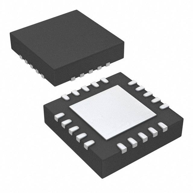
The TPS22980 is available in a 4mm x 4mm x 1mm QFN package.
RSVD
Figure 1. Typical Application
1
Please be aware that an important notice concerning availability, standard warranty, and use in critical applications of
Texas Instruments semiconductor products and disclaimers thereto appears at the end of this data sheet.
PRODUCTION DATA information is current as of publication date.
Products conform to specifications per the terms of the Texas
Instruments standard warranty. Production processing does not
necessarily include testing of all parameters.
Copyright © 2011–2013, Texas Instruments Incorporated
�TPS22980
SLVSB61C – DECEMBER 2011 – REVISED SEPTEMBER 2013
www.ti.com
These devices have limited built-in ESD protection. The leads should be shorted together or the device placed in conductive foam
during storage or handling to prevent electrostatic damage to the MOS gates.
TOP VIEW / FOOTPRINT
18
V3P3
V3P3
RSVD
OUT
GND
OUT
HV_EN
GND
GND
GND
GND
EN
11
1
2
3
4
5
Exposed
Pad
(Connect to GND)
10
ISET_S0
V3P3
20
9
ISET_S3
V3P3
19
GND
GND
GND
EN
ISET_V3P3
9
ISET_S3
VHV
RSVD
16
10
ISET_S0
6
GND
8
17
20
5
VHV
S0
7
4
7
VHV
19
3
VHV
18
ISET_V3P3
2
6
V3P3OUT
8
1
Exposed
Pad
(Connect to GND)
15
14
13
12
11
HV_EN
V3P3OUT
12
OUT
17
13
GND
S0
14
OUT
16
15
RSVD
RSVD
BOTTOM VIEW
Package Size: 4mm x 4mm x 1mm height, Pad Pitch: 0.5mm
PIN FUNCTIONS
PIN
NO.
DESCRIPTION
NAME
1
2
GND
Device ground
EN
Device Enable.
VHV
High voltage power supply input. Place a minimum of 0.1µF capacitor as close to this pin as possible.
8
ISET_V3P3
Sets the current limit for V3P3. Place resistor between this pin and GND. See Equation 1 to calculate resistor
value.
9
ISET_S3
Sets the current limit for VHV in S3 mode. Place resistor between this pin and GND. See Equation 1 to
calculate resistor value.
10
ISET_S0
Sets the current limit for VHV in S0 mode. Place resistor between this pin and GND. See Equation 1 to
calculate resistor value.
11
3
4
5
6
7
HV_EN
High voltage output enable.
12, 14
OUT
Power output. Place a minimum of 1µF capacitor as close to this pin as possible.
13
GND
Device ground.
RSVD
Reserved. Must Tie to GND.
17
S0
When this pin is asserted, the device is put in S0 mode. Otherwise the device operates in S3 mode.
18
V3P3OUT
3.3V bypass output. Place a minimum of 0.1µF capacitor as close to this pin as possible.
V3P3
3.3V power supply input. Place a minimum of 0.1µF capacitor as close to this pin as possible.
15
16
19
20
EP
2
GND
Submit Documentation Feedback
Copyright © 2011–2013, Texas Instruments Incorporated
Product Folder Links :TPS22980
�TPS22980
www.ti.com
SLVSB61C – DECEMBER 2011 – REVISED SEPTEMBER 2013
ABSOLUTE MAXIMUM RATINGS
over operating free-air temperature range (unless otherwise noted) (1)
(2)
VALUE
(3)
–0.3 to 3.6
Input voltage range on EN, HVEN, ISET_V3P3, ISET_S0, ISET_S3, S0 (3)
–0.3 to V3P3+0.3
Input voltage range on V3P3 (VDD)
VI
Input voltage range on VHV (3)
–0.3 to 20
Output voltage range at OUT (3)
–0.3 to 20
UNIT
V
Output voltage range at V3P3OUT (3)
–0.3 to V3P3+0.3
TA
Operating ambient temperature range
–40 to 85
°C
TJ
Maximum operating junction temperature
110
°C
–65 to 150
°C
(MAX)
Tstg
Storage temperature range
ESD Rating
(1)
(2)
(3)
Charge Device Model (JESD 22 C101)
500
V
2
kV
Human Body Model (JESD 22 A114)
Stresses beyond those listed under absolute maximum ratings may cause permanent damage to the device. These are stress ratings
only, and functional operation of the device at these or any other conditions beyond those indicated under recommended operating
conditions is not implied. Exposure to absolute–maximum–rated conditions for extended periods may affect device reliability.
In applications where high power dissipation and/or poor package thermal resistance is present, the maximum ambient temperature may
have to be de-rated. Maximum ambient temperature [TA(max)] is dependent on the maximum operating junction temperature [TJ(max)], the
maximum power dissipation of the device in the application [PD(max)], and the junction-to-ambient thermal resistance of the part/package
in the application (θJA), as given by the following equation: TA(max) = TJ(max) – (θJA × PD(max))
All voltage values are with respect to network ground terminal.
THERMAL INFORMATION
TPS22980
THERMAL METRIC (1)
RGP
UNITS
16 PINS
θJA
Junction-to-ambient thermal resistance
38.9
θJCtop
Junction-to-case (top) thermal resistance
30.7
θJB
Junction-to-board thermal resistance
11.5
ψJT
Junction-to-top characterization parameter
0.4
ψJB
Junction-to-board characterization parameter
11.4
θJCbot
Junction-to-case (bottom) thermal resistance
2.2
(1)
°C/W
For more information about traditional and new thermal metrics, see the IC Package Thermal Metrics application report, SPRA953.
Submit Documentation Feedback
Copyright © 2011–2013, Texas Instruments Incorporated
Product Folder Links :TPS22980
3
�TPS22980
SLVSB61C – DECEMBER 2011 – REVISED SEPTEMBER 2013
www.ti.com
RECOMMENDED OPERATING CONDITIONS
V3P3
Supply voltage range
VHV
MIN
MAX
3.0
3.6
UNIT
4.5
19.8
V
0
500
mA
V
ILIM3P3OUT
V3P3OUT Switch current range
VIH
Input logic high
EN, HV_EN, S0
V3P3-0.6
V3P3
VIL
Input logic low
EN, HV_EN, S0
0
0.6
V
RSET_V3P3
3.3V switch current limit set resistance
25.3
402
kΩ
RSET_S0
VHV switch current limit in S0 mode set resistance
25.3
402
kΩ
RSET_S3
VHV switch current limit in S3 mode set resistance
25.3
402
kΩ
V
ELECTRICAL CHARACTERISTICS
Unless otherwise noted the specification applies over the VDD range and operating junction temp –40°C ≤ TJ ≤ 85°C. Typical
values are for V3P3 = 3.3V, VHV = 15V, and TJ = 25°C.
PARAMETER
TEST CONDITIONS
MIN
TYP
3
3.3
MAX
UNIT
POWER SUPPLIES AND CURRENTS
V3P3
V3P3 Input voltage range
VHV
VHV Input voltage range
3.6
V
19.8
V
IVHVACT
Active quiescent current from VHV
HV_EN = 1, EN = 1
IVHVSD
Shutdown leakage current from VHV
HV_EN = 0, EN = 0 or 1
150
µA
30
IDDACT
Active quiescent current from V3P3
µA
EN = 1, HV_EN = 0
200
IDDACTHV
µA
Active quiescent current from V3P3
EN = 1, HV_EN = 1
150
µA
IDDSD
Shutdown Quiescent Current from V3P3
EN = 0, OUT = 0V
10
µA
IDIS
OUT Discharge Current
EN = 1, VHV = 5V
HV_EN = 1 → 0
10
mA
IIN
HV_EN, EN, S0, S3 Input pin leakage
V=0V
1
µA
V = V3P3
1
µA
4.5
5
SWITCH AND RESISTANCE CHARACTERISTICS
RSHV
VHV Switch resistance
VHV = 5 V to 18V, IVHV = 1.5 A
250
mΩ
RS3P3
V3P3 Switch resistance
V3P3 = 3.3 V, IV3P3 = 1.5 A
250
mΩ
RS3P3BYP
V3P3 Bypass switch resistance
V3P3 = 3.3 V, IV3P3 = 500 mA
500
mΩ
ROUTDIS
OUT Pulldown resistance when disabled
EN = 0
1.5
2.5
4
kΩ
VHV Input Falling
3.6
4
VOLTAGE THESHOLDS
VHVUVLO
VHV Under voltage lockout
V3P3UVLO
V3P3 Under voltage lockout
VHV Input Rising
V3P3 Input Falling
4
1.8
V3P3 Input Rising
4.3
2.25
2.25
2.5
120
130
V
V
THERMAL SHUTDOWN
TSD
Shutdown Temperature
TSDHYST
Shutdown Hysteresis
4
110
10
Submit Documentation Feedback
°C
°C
Copyright © 2011–2013, Texas Instruments Incorporated
Product Folder Links :TPS22980
�TPS22980
www.ti.com
SLVSB61C – DECEMBER 2011 – REVISED SEPTEMBER 2013
ELECTRICAL CHARACTERISTICS (continued)
Unless otherwise noted the specification applies over the VDD range and operating junction temp –40°C ≤ TJ ≤ 85°C. Typical
values are for V3P3 = 3.3V, VHV = 15V, and TJ = 25°C.
PARAMETER
TEST CONDITIONS
MIN
TYP
MAX
RSET_S0, 3 = 402 kΩ
100
110
150
RSET_S0, 3 = 80.6 kΩ
495
525
555
RSET_S0, 3 = 26.7 kΩ
1515
1575
1635
RSET_V3P3 = 402 kΩ
100
110
150
UNIT
CURRENT LIMIT
ILIMHV
ILIM3P3
VHV Switch current limit state S0 or S3
V3P3 Switch current limit
mA
RSET_V3P3 = 80.6 kΩ
495
525
555
RSET_V3P3 = 26.7 kΩ
1515
1575
1635
mA
10
27
45
mA
100
µS
IREV3P3
V3P3 Switch Reverse Current Limit
TV3P3RC
V3P3 Switch Reverse Current Response
Time
VOUT = V3P3 → V3P3 + 20mV
TVHVSC
VHV Switch short circuit response time
COUT = 20 pF
8
µs
TV3P3SC
V3P3 Switch short circuit response time
COUT = 20 pF
8
µs
TRANSITION DELAYS
T3P3OFF
VHV to V3P3 off time
COUT = 1.1µF, EN = 1, HV_EN = 1→0
6
ms
T0-3.3V
0V to 3.3V ramp time
COUT ≤ 20 pF
6
ms
T3.3V-VHV
3.3V to VHV ramp time
COUT ≤ 20 pF
6
ms
TVHV-3.3V
VHV to 3.3V ramp time
COUT ≤ 20 pF
23
ms
TLIM
Overcurrent response time
COUT ≤ 20 pF
0.5
ms
FUNCTIONAL BLOCK DIAGRAM
6
VHV
3
7
1
VTHV
10
9
11
5
S0
ISET_S0
Switch
CTRL
Logic
ISET_S3
ISET_V3P3
OUT
OUT
EN
12
14
13
V3P3
19
2
8
HV_EN
Thermal
shutdown
20
17
V3P3OUT
EN
18
4
Submit Documentation Feedback
Copyright © 2011–2013, Texas Instruments Incorporated
Product Folder Links :TPS22980
5
�TPS22980
SLVSB61C – DECEMBER 2011 – REVISED SEPTEMBER 2013
www.ti.com
APPLICATION INFORMATION
CURRENT LIMIT
The TPS22980 provides current limiting in the power switches. Both the VHV supply current limit and the V3P3
supply current limit are adjustable by external resistors.
Figure 2 shows a simplified view of the TPS22980 current limit function. Both the VHV supply current limit and
the V3P3 supply current limit are adjustable by external resistors.
VHV
4.5 - 18V
IREF _HV
Switch
CTRL
Logic
OUT
I REF_V3P3
3.3V
Figure 2. Simplified Current Limit Diagram
The current limit thresholds, IREF_HV and IREF_V3P3, are set with three external resistors as shown in Figure 3.
When the TPS22980 is passes the V3P3 voltage, the current limit is set by RISET_V3P3. The VHV path has two
modes that support two different current limits which are selected by the S0 pin. When S0 is asserted high,
RISET_S0 sets the current limit. When S0 is low, RISET_S3 sets the current limit. This allows the system to have two
separate VHV current limits for different modes such as active and sleep.
RSET_V3P3
ISET_V3P3
RSET_S3
ISET_S3
RSET_S0
ISET_S0
Figure 3. External RSET Resistances to Set Current Limits
CURRENT LIMIT THRESHOLD
6
Submit Documentation Feedback
Copyright © 2011–2013, Texas Instruments Incorporated
Product Folder Links :TPS22980
�TPS22980
www.ti.com
SLVSB61C – DECEMBER 2011 – REVISED SEPTEMBER 2013
60%
1800
1600
50%
% - variance from min - A
ILIMHV/V3P3 - A
1400
1200
1000
800
min
typ
max
600
400
40%
30%
min
typ
max
20%
10%
200
0
0%
0
50
100
150
200
250
300
RISET_S0/S3/V3P3 - W
350
400
Figure 4. ILIM vs RSET for VHV and V3P3
450
0
50
100
150
200
250
300
RISET_S0/S3/V3P3 - W
350
400
450
Figure 5. Percent Variance from min ILIM vs RSET
Figure 4 shows the minimum, typical, and maximum current limit for either supply versus its corresponding RISET
value. Equation 1 is used to determine the RISET needed to set a minimum ILIM for a given supply and mode.
Figure 5 shows the approximate variation from the set minimum ILIM value to the typical and maximum ILIM
values.
RISET =
40 kΩ ´ Amps
ILIMmin
(1)
where:
RISET = external resistor used to set the current limit for V3P3, VHV (S0), or VHV (S3), and
ILIMmin = current limit for V3P3, VHV (S0), or VHV (S3) set by the external RISET resistor.
Each resistor is placed between the corresponding ISET pin and GND, as shown in Figure 3, providing a
minimum current limit between 100mA and 1.5A.
TRANSITION DELAYS
Output transitions of the TPS22980 voltages are shown in Figure 6. When the device transitions from VHV to
V3P3 at the output, the power switches both turn off until the output falls to near the V3P3 voltage. During this
time, a discharge current (IDIS) pulls OUT down. If a load on the line is also pulling OUT down, the output can
drop to 0V due to the switch off time of T3P3OFF. Figure 7 shows the voltage drop on the output during this
transition with no output capacitance.
Submit Documentation Feedback
Copyright © 2011–2013, Texas Instruments Incorporated
Product Folder Links :TPS22980
7
�TPS22980
SLVSB61C – DECEMBER 2011 – REVISED SEPTEMBER 2013
www.ti.com
Figure 6. Allowable Voltage Transitions
Figure 7. Voltage Drop During Transitions from VHV
DIGITAL CONTROL SIGNALS
The voltage at OUT is controlled by two digital logic input signals, EN and HV_EN. HV_EN controls the state of
the VHV switch and EN controls the state of V3P3 switch. Table 1 lists the possible output states given the
conditions of the digital logic signals. State PD indicates a pulldown resistance of ROUTDIS to GND.
Table 1. Output State of OUT Given the States EN and
HV_EN
8
EN
HV_EN
OUT
0
0
PD
0
1
PD
1
0
V3P3
1
1
VHV
Submit Documentation Feedback
Copyright © 2011–2013, Texas Instruments Incorporated
Product Folder Links :TPS22980
�TPS22980
www.ti.com
SLVSB61C – DECEMBER 2011 – REVISED SEPTEMBER 2013
Figure 8 shows possible combinations of EN and HV_EN controlling OUT of the TPS22980.
EN
HV_EN
HV_UVLO
HV_EN & HV_UVLO
S3P3
SHV
18 V
OUT
3.3 V
3.3 V
0V
IDIS
Figure 8. Logic Waveforms Displaying the Transition Between VHV and V3P3
OVER-CURRENT LIMIT AND SHORT CIRCUIT PROTECTION
When the load at OUT attempts to draw more current than the limit set by the external RISET resistors for the
V3P3 switch and VHV switch (for both S0 and S3 modes), the device will operate in a constant current mode
while lowering the output voltage. Figure 9 shows the delay, tLIM, which occurs when an over-current fault is
detected until the output current is lowered to ILIMHV tolerances for VHV or ILIM3V3 tolerances for V3P3 as
shown in Figure 4.
Output
Voltage
t
Load
Current
OC Limit
tLIM delay
Figure 9. Overcurrent Output Response
All short circuit conditions are treated as over-current conditions. In the event of a short circuit, the device will
limit the output current to the corresponding RSET value and continue to do so until thermal shutdown is
encountered or the short circuit condition is removed.
Submit Documentation Feedback
Copyright © 2011–2013, Texas Instruments Incorporated
Product Folder Links :TPS22980
9
�TPS22980
SLVSB61C – DECEMBER 2011 – REVISED SEPTEMBER 2013
www.ti.com
Reverse Current Protection
Reverse current protection for the V3P3 supply to OUT triggers at IREV3P3 causing the V3P3 supply switch to
open. When the HV_EN signal is not asserted and reverse current protection is triggered, a discharge current
source is turned on to bring the output voltage to 3.3V nominal.
Thermal Shutdown
The device enters thermal shutdown when junction temperature reaches TSD. The device will resume the
previous state on power up once the junction temperature has dropped by 10°C. Connect thermal vias to the
exposed GND pad underneath the device package for improved thermal diffusion.
UVLO
When the VHV rail reaches the under-voltage lockout threshold of VHVUVLO while HV_EN is high, the device will
switch back to V3P3. Once the UVLO condition has cleared, the device will switch to VHV again. When the V3P3
rail reaches the under-voltage lockout threshold of V3P3UVLO, regardless of the states of any digital logic controls,
the device will open all switches and enter a reset condition.
Input Inductive Bounce at Short Circuit
When the TPS22980 is operating at high currents and high input voltage on VHV, a short circuit condition can
cause the input to exceed the maximum safe operating condition for VHV. When a significant inductance is
present at the VHV input, sudden turn off of current through the device may produce a large enough inductive
voltage bounce that exceeds the maximum safe operating condition and may damage the TPS22980. To prevent
this, reduce any inductance at the input. Input capacitors, such as 4.7µF, can reduce the supply bounce and are
recommended.
Single Point Failure Protection
The TPS22980 current limits are set by the RISET resistances. Shorting one of these resistance would result in a
single point failure that removes the current limiter for that particular input and mode. Without current limiting, an
excessive current load may damage the TPS22980 and the system. To prevent a single point failure from
occurring, the RISET resistances can be divided into two series resistances each as shown in Figure 10. Failure
of a single resistance will not result in runaway current and damage.
Figure 10. RISET Division to Prevent Single Point Failure
10
Submit Documentation Feedback
Copyright © 2011–2013, Texas Instruments Incorporated
Product Folder Links :TPS22980
�TPS22980
www.ti.com
SLVSB61C – DECEMBER 2011 – REVISED SEPTEMBER 2013
REVISION HISTORY
Changes from Original (December 2011) to Revision A
Page
•
Changed Typical Application figure. ..................................................................................................................................... 1
•
Added bottom view pin out information. ............................................................................................................................... 2
•
Updated Pin Functions Table. .............................................................................................................................................. 2
•
Added reverse current and thermal shutdown parameters to the ELECTRICAL CHARACTERISTICS table. .................... 4
•
Updated the APPLICATION INFORMATION section. .......................................................................................................... 6
Changes from Revision A (February 2012) to Revision B
•
Page
Changed bottom view pin out information. ........................................................................................................................... 2
Changes from Revision B (April 2012) to Revision C
Page
•
Removed ordering information table. .................................................................................................................................... 2
•
Added ROUTDIS parameter to the Electrical Characteristics table. ......................................................................................... 4
•
Updated the DIGITAL CONTROL SIGNALS section. .......................................................................................................... 8
Submit Documentation Feedback
Copyright © 2011–2013, Texas Instruments Incorporated
Product Folder Links :TPS22980
11
�PACKAGE OPTION ADDENDUM
www.ti.com
10-Dec-2020
PACKAGING INFORMATION
Orderable Device
Status
(1)
Package Type Package Pins Package
Drawing
Qty
Eco Plan
(2)
Lead finish/
Ball material
MSL Peak Temp
Op Temp (°C)
Device Marking
(3)
(4/5)
(6)
TPS22980RGPR
ACTIVE
QFN
RGP
20
3000
RoHS & Green
NIPDAU
Level-2-260C-1 YEAR
-40 to 85
PS22980
(1)
The marketing status values are defined as follows:
ACTIVE: Product device recommended for new designs.
LIFEBUY: TI has announced that the device will be discontinued, and a lifetime-buy period is in effect.
NRND: Not recommended for new designs. Device is in production to support existing customers, but TI does not recommend using this part in a new design.
PREVIEW: Device has been announced but is not in production. Samples may or may not be available.
OBSOLETE: TI has discontinued the production of the device.
(2)
RoHS: TI defines "RoHS" to mean semiconductor products that are compliant with the current EU RoHS requirements for all 10 RoHS substances, including the requirement that RoHS substance
do not exceed 0.1% by weight in homogeneous materials. Where designed to be soldered at high temperatures, "RoHS" products are suitable for use in specified lead-free processes. TI may
reference these types of products as "Pb-Free".
RoHS Exempt: TI defines "RoHS Exempt" to mean products that contain lead but are compliant with EU RoHS pursuant to a specific EU RoHS exemption.
Green: TI defines "Green" to mean the content of Chlorine (Cl) and Bromine (Br) based flame retardants meet JS709B low halogen requirements of


 工商网监
湘ICP备2023018690号
工商网监
湘ICP备2023018690号
