ON Semiconductor
Is Now
To learn more about onsemi™, please visit our website at
www.onsemi.com
onsemi and and other names, marks, and brands are registered and/or common law trademarks of Semiconductor Components Industries, LLC dba “onsemi” or its affiliates and/or
subsidiaries in the United States and/or other countries. onsemi owns the rights to a number of patents, trademarks, copyrights, trade secrets, and other intellectual property. A listing of onsemi
product/patent coverage may be accessed at www.onsemi.com/site/pdf/Patent-Marking.pdf. onsemi reserves the right to make changes at any time to any products or information herein, without
notice. The information herein is provided “as-is” and onsemi makes no warranty, representation or guarantee regarding the accuracy of the information, product features, availability, functionality,
or suitability of its products for any particular purpose, nor does onsemi assume any liability arising out of the application or use of any product or circuit, and specifically disclaims any and all
liability, including without limitation special, consequential or incidental damages. Buyer is responsible for its products and applications using onsemi products, including compliance with all laws,
regulations and safety requirements or standards, regardless of any support or applications information provided by onsemi. “Typical” parameters which may be provided in onsemi data sheets and/
or specifications can and do vary in different applications and actual performance may vary over time. All operating parameters, including “Typicals” must be validated for each customer application
by customer’s technical experts. onsemi does not convey any license under any of its intellectual property rights nor the rights of others. onsemi products are not designed, intended, or authorized
for use as a critical component in life support systems or any FDA Class 3 medical devices or medical devices with a same or similar classification in a foreign jurisdiction or any devices intended for
implantation in the human body. Should Buyer purchase or use onsemi products for any such unintended or unauthorized application, Buyer shall indemnify and hold onsemi and its officers, employees,
subsidiaries, affiliates, and distributors harmless against all claims, costs, damages, and expenses, and reasonable attorney fees arising out of, directly or indirectly, any claim of personal injury or death
associated with such unintended or unauthorized use, even if such claim alleges that onsemi was negligent regarding the design or manufacture of the part. onsemi is an Equal Opportunity/Affirmative
Action Employer. This literature is subject to all applicable copyright laws and is not for resale in any manner. Other names and brands may be claimed as the property of others.
�FGBS3040E1-F085
Integrated Smart Ignition Coil Driver
Features
Description
The FGBS3040E1-F085 is designed to directly drive an
ignition coil and control the current and spark event of
the coil. The coil current is controlled via the
input/diagnostic pin. When the input is driven high, the
IGBT is enabled to start charging the coil. The
FGBS3040E1-F085 w ill sink a current (IIN1) into the
input to denote this condition. When the collector current
increases to Icthr the input current into the
FGBS3040E1-F085 is reduced to IIN2 indicating the
collector current has reached this level. An input filter
suppresses input signals of less then 13 µsec in
duration. A Max Dw ell timer is included in the
FGBS3040E1-F085 w hich w ill turn off the IGBT if the
input stays active for longer then the programmed time.
This time interval can be modified through an external
capacitor. When the Max Dw ell timer is exceeded, the
FGBS3040E1-F085 w ill enter a Soft-Shut-Dow n mode
(SSD) slow ly dropping the collector current thereby
discharging the coil such as to inhibit a spark event.
Once the soft shutdow n operation has started, any
transitions on the input signal are ignored until after
completion of the soft shutdow n function. The
FGBS3040E1-F085 w ill also limit the collector current of
the IGBT to Ic(lim) during charging.
400V 300mJ N Channel Ignition IGBT
Control Input buffering
Input spike filter of typical 13us
Operation from Ignition or Battery line
Ground shift tolerance +/- 1.5V
Programmable maximum dw ell time
Current programmable bidirectional
Input/Diagnostic pin
Collector Current limit typical 16.5A
Soft Shutdow n of Collector Current after Max Dw ell
Applications
Coil on Plug Ignition systems
General ignition systems
© 2016 Semiconductor Components Industries, LLC.
September-2017, Rev. 2
Publication Order Number:
FGBS3040E1-F085/D
FGBS3040E1-F085 — Integrated Smart Ignition Coil Driver
April 2016
�Figure 1.
Block Diagram of FGBS3040E1-F085
Typical Application
Figure 2.
Typical Ignition Coil Driver Application
www.onsemi.com
2
FGBS3040E1-F085 — Integrated Smart Ignition Coil Driver
Block Diagram
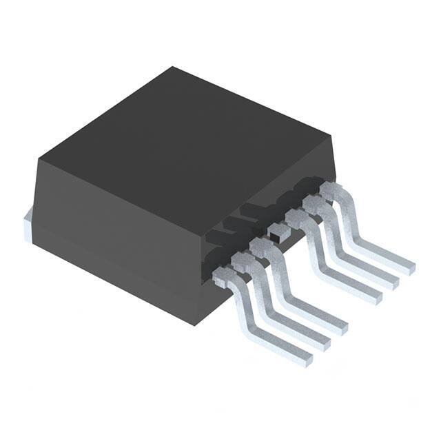
�The FGBS3040E1-F085 is assembled in a 7 lead TO263 package
TO263-7L
Pin Assignm ent (Top Through View )
Pin1
Pin2
Pin3
Pin4/Tab
Pin5
Pin6
Pin7
GND
Vbat
IN/IFL
COL
NC
CSSD
RA
Emitter and control IC ground
Supply voltage
Input and diagnostic (bidirectional)
IGBT collector output
NC
Maximum dw ell time and Soft-Shut-Dow n current output (to external capacitor)
Input reference current output (to external resistor)
Absolute Maximum Ratings1
Stresses exceeding the absolute maximum ratings may damage the device. The device may not function or be
operable above the recommended operating conditions and stressing the parts to these levels is not recommended.
In addition, extended exposure to stresses above the recommended operating conditions may affect device reliability.
The absolute maximum ratings are stress ratings only.
Parameter
Symbol
Voltage at V bat pin (excl. EMC transients)
V bat
Values
-0.3… 28
Unit
V
Voltage at IN/IFL pin
V IN1
- 1... 16
V
Voltage at A & CSSD pins
V IN2
- 0.3... 6
V
Collector Emitter Voltage (V IN = 0V) Ic=10mA
V C-GND(CL)
450
V
Operating Temperature Range
TJ
-40... +175
°C
Storage Temperature Range
TSTG
-40... +175
°C
Output Current
IC(lim)
Self Clamped Inductive Sw itched Energy @Tj = 25°C
IC(lim) max
A
EAS
300
mJ
Self Clamped Inductive Sw itched Energy @Tj = 150°C
EAS
170
mJ
Maximum pow er dissipation (continuous) from TC = 25°C
Pmax
150
W
Thermal Resistance junction–case (typical)
RΘJC
1
°C /W
Electrostatic Discharge Voltage (Human Body Model)
V ESD (pin to pin)
2
kV
according to MIL STD 883D, method 3015.7 and EOS/ESD
assn. standard S5.1 - 1993
V ESD (CE)
4
kV
www.onsemi.com
3
FGBS3040E1-F085 — Integrated Smart Ignition Coil Driver
Pin Configuration
�The Recommended Operating Conditions table defines the conditions for actual device operation. Recommended
operating conditions are specified to ensure optimal performance. ON Semiconductor does not recommend
exceeding them or designing to Absolute Maximum Ratings.
Symbol
Parameter
IIN2
Typ.
Max.
Unit
-0.3
Input low voltage
2.85
V
Input high voltage
V bat = 5 to 28 V;
TJ= - 40 °C to +
175 °C (unless
otherw ise specified)
V bat = 5 to 28 V;
T = - 40 °C to +
Input voltage hysteresis J
175 °C (unless
otherw ise specified)
See fig 8 for typical
values vs Ra
Input current (IC <
(Measured w ith
IcTHR)
11.5k_, ±1%
resistor on A pin)
See fig 8 for typical
values vs Ra
Input current (IC >
(Measured w ith
IcTHR)
11.5k_, ±1%
resistor on A pin)
0.25
V
VINH
IIN1
Min.
V bat = 5 to 28 V;
TJ= - 40 °C to +
175 °C (unless
otherw ise specified)
VINL
VINHys
Conditions
2.05
V
16
18
20
mA
6
7.1
10
mA
IIN1
Input current (IC < Ic THR) (Note 1)
4.2
mA
IIN2
Input current (IC > Ic THR) (Note 1)
1.8
mA
Coss
Output capacitance
70
pF
V C-GND = 25 V, V IN =
0 V, f = 1 MHz
Ic THR
Collector current
feedback (IFL)
threshold 25 C to
175C
(Measured w ith
11.5k_, ±1%
resistor on A pin)
4.3
Ic THR
Collector current
feedback (IFL)
threshold -40C
(Measured w ith
11.5k_, ±1%
resistor on A pin)
Note 3
5.3
6.8
A
4.3
7.3
A
5.2
200
kΩ
RA
Resistor for input
reference current
CSSDMIN
Minimum dwell time
capacitor
TDMAX
Maximum dwell time (CSSDEXT=10nF)
19
23
28
ms
ISLEW
Soft-Shut-Down slew (Ic: 90% -20%IL)
0.7
1.5
2.5
A/ms
ICSSD1
CSSD Pin current for
1.0
1.25
1.5
µA
2.2
rate
TDMAX
www.onsemi.com
4
nF
FGBS3040E1-F085 — Integrated Smart Ignition Coil Driver
Recommended Operating Conditions
�Symbol
Parameter
Conditions
Min. Typ. Max. Unit
Vbat1
Operating voltage
Coil sw itching
4
28
V
Vbat2
Operating voltage
All functions
5
28
V
Ibat
Supply current
(TJ=175°C, Vbat = 28V, RA open,
IN/IFL = 5V)
5
mA
VC-
Collector emitter clamping
voltage
(IC = 10 mA)
GND(CL)
IC(leak)
Collector leakage current
450
V
(TJ=175°C,V C-GND=300 V)
30
µA
Collector emitter saturation
voltage (Ic=10A, Tj=175°C)
Collector emitter saturation voltage
(Ic=10A, Tj=175°C)
1.8
V
Current Limit
(Note 2)
19
A
Current fall time
Current fall time
15
µs
Tspike
Input spike filter delay on rising
and falling edge of IN/IFL
Input spike filter delay on rising and
falling edge of IN/IFL
TD1
Turn on delay time (Time from
VIN/IFL=4.0 V to Vcgnd=Vbat/2)
Turn on delay time (Time from
VIN/IFL=4.0 V to Vc-gnd=Vbat/2)
10
13
26
µs
Turn off delay time (Time from
VIN/IFL=0.5 V to Vcgnd=Vbat/2)
Turn off delay time (Time from
VIN/IFL=0.5 V to Vc-gnd=Vbat/2)
10
17
28
µs
VCGND(SA
390
T)
IC(lim)
Tfall
TD2
14
Notes:
1. Measured w ith open or shorted RA pin
2. Range can be varied betw een typ. 8-16.5A or can be eliminated w ith metal mask options
3. Icth max < 7.3A- 0.0077*(T+40C) for Tj from -40 to 25C
www.onsemi.com
5
µs
13
FGBS3040E1-F085 — Integrated Smart Ignition Coil Driver
Electrical Characteristics
�Input and spike filter
When the input signal voltage reaches VINH, the coil
current w ill be sw itched on through the IGBT. When the
input voltage goes below VINL, the coil current through
the IGBT w ill be turned off. If the ignitor is in SSD mode,
the input signal control is disabled.
After a SSD
sequence input control w ill be re-enabled after the input
has reached a valid low . Positive and negative spikes of
< Tspike duration at the input line w ill be filtered out and
w ill not turn on/off the IGBT.
If the CSSD capacitor has a value of < 2.2nF or the
CSSD pin is shorted to ground, the maximum dw ell time
and SSD functions w ill be disabled.
Bidirectional input / diagnosis pin
The pin IN/IFL has a double function. It is used as input
pin to control the pow er stage (on/off) and as output pin
that delivers diagnostic information about the collector
current level (current flag).
b) The IN/IFL pin sinks constantly a current of IIN1.
When the input voltage is above VINH and the collector
current exceeds the IcTHR threshold, the current flag is
set by sw itching a current sink at the bidirectional IN/IFL
pin to IIN2 (see Fig.4)
c) If resistor RA has a value 200k, IIN1 and
IIN2 w ill be set to their default values.
Figure 5: Dw ell tim e and Soft-Shut-Dow n
35
30
TDMAX[ms]
a) If the input voltage reaches VINH, the pow er stage is
turned on. If the input voltage is below VINL, the pow er
stage is turned off.
25
20
15
10
4
5
6
7
8
9
10
11
12
13
14
15
Cext [nF]
Figure 6: TDMAX as function of external CSSD
capacitor
Figure 7 show s the IN1 and IN2 currents in dependency
of the IRA current.
Figure 4: Bidirectional IN/INFL Diagnostic Pin
Maximum dwell time and softshutdown (SSD)
When the IGBT is turned on, a delay timer, dependent
on the value of the external CSSD capacitor (see Fig.6),
is started. If a valid falling edge has not been received
after the time TDMAX, the IGBT w ill be turned off slow ly
as show n in Fig.5. The coil current w ill not exceed a
slew rate of typical 1.2A/ms. If a valid falling edge is
received after the time TDMAX, the edge w ill be ignored
and the soft shutdow n w ill be completed. The IGBT
cannot be subsequently turned on until a valid rising
edge is detected.
Figure 7: Typical IN1 and IN2 Currents vs Ra
The value for RA can be determined by the formula:
RA = (1.24/IRA)-750.
www.onsemi.com
6
FGBS3040E1-F085 — Integrated Smart Ignition Coil Driver
Functional Description
�Center Diagram (fill the page as much as looks reasonable & center in the space)
Verify it is the CURRENT version of the Marketing Outline Draw ing (MOD)!
The official draw ings are archived in Documentum, so you can get copies there.
You can verify the current draw ing at: http://w w w .fairchildsemi.com/dw g/
Figure 3.
Packaging Outline and Dim ensions (TO263A07 Rev4)
Package drawings are provided as a service to customers considering ON Semiconductor components. Drawings may change in
any manner without notice. Please note the revision and/or date on the drawing and contact a ON Semiconductor representative to
verify or obtain the most recent revision. Package specifications do not expand the terms of ON Semiconductor’s worldwide terms
and conditions, specifically the warranty therein, which covers ON Semiconductor products.
www.onsemi.com
7
FGBS3040E1-F085 — Integrated Smart Ignition Coil Driver
Physical Dimensions
�FGBS3040E1-F085 — Integrated Smart Ignition Coil Driver
ON Semiconductor and the ON Semiconductor logo are trademarks of Semiconductor Components Industries, LLC dba ON Semiconductor or its subsidiaries in the
United States and/or other countries. ON Semiconductor owns the rights to a number of patents, trademarks, copyrights, trade secrets, and other intellectual property. A
listing of ON Semiconductor’s product/patent coverage may be accessed at www.onsemi.com/site/pdf/Patent-Marking.pdf. ON Semiconductor reserves the right to make
changes without further notice to any products herein. ON Semiconductor makes no warranty, representation or guarantee regarding the suitability of its products for any
particular purpose, nor does ON Semiconductor assume any liability arising out of the application or use of any product or circuit, and specifically disclaims any and all
liability, including without limitation special, consequential or incidental damages. Buyer is responsible for its products and applications using ON Semiconductor
products, including compliance with all laws, regulations and safety requirements or standards, regardless of any support or applications information provided by
ON Semiconductor. “Typical” parameters which may be provided in ON Semiconductor data sheets and/or specifications can and do vary in different applications and
actual performance may vary over time. All operating parameters, including “Typicals” must be validated for each customer application by customer’s technical experts.
ON Semiconductor does not convey any license under its patent rights nor the rights of others. ON Semiconductor products are not designed, intended, or authorized for
use as a critical component in life support systems or any FDA Class 3 medical devices or medical devices with a same or similar classification in a foreign jurisdiction or
any devices intended for implantation in the human body. Should Buyer purchase or use ON Semiconductor products for any such unintended or unauthorized
application, Buyer shall indemnify and hold ON Semiconductor and its officers, employees, subsidiaries, affiliates, and distributors harmless against all claims, costs,
damages, and expenses, and reasonable attorney fees arising out of, directly or indirectly, any claim of personal injury or death associated with such unintended or
unauthorized use, even if such claim alleges that ON Semiconductor was negligent regarding the design or manufacture of the part. ON Semiconductor is an Equal
Opportunity/Affirmative Action Employer. This literature is subject to all applicable copyright laws and is not for resale in any manner.
PUBLICATION ORDERING INFORMATION
LITERATURE FULFILLMENT:
Literature Distribution Center for ON Semiconductor
19521 E. 32nd Pkwy, Aurora, Colorado 80011 USA
Phone: 303-675-2175 or 800-344-3860 Toll Free USA/Canada
Fax : 303-675-2176 or 800-344-3867 Toll Free USA/Canada
Email: orderlit@onsemi.com
N. Amer ican Technical Support: 800-282-9855 Toll Free
USA/Canada.
Eur ope, Middle East and Afr ica Technical Support:
Phone: 421 33 790 2910
Japan Customer Focus Center
Phone: 81-3-5817-1050
www.onsemi.com
8
ON Semiconductor Website: www.onsemi.com
Or der Literature: http://www.onsemi.com/orderlit
For additional information, please contact your local
Sales Representative
�


 工商网监
湘ICP备2023018690号
工商网监
湘ICP备2023018690号
