ON Semiconductor
Is Now
To learn more about onsemi™, please visit our website at
www.onsemi.com
onsemi and and other names, marks, and brands are registered and/or common law trademarks of Semiconductor Components Industries, LLC dba “onsemi” or its affiliates and/or
subsidiaries in the United States and/or other countries. onsemi owns the rights to a number of patents, trademarks, copyrights, trade secrets, and other intellectual property. A listing of onsemi
product/patent coverage may be accessed at www.onsemi.com/site/pdf/Patent-Marking.pdf. onsemi reserves the right to make changes at any time to any products or information herein, without
notice. The information herein is provided “as-is” and onsemi makes no warranty, representation or guarantee regarding the accuracy of the information, product features, availability, functionality,
or suitability of its products for any particular purpose, nor does onsemi assume any liability arising out of the application or use of any product or circuit, and specifically disclaims any and all
liability, including without limitation special, consequential or incidental damages. Buyer is responsible for its products and applications using onsemi products, including compliance with all laws,
regulations and safety requirements or standards, regardless of any support or applications information provided by onsemi. “Typical” parameters which may be provided in onsemi data sheets and/
or specifications can and do vary in different applications and actual performance may vary over time. All operating parameters, including “Typicals” must be validated for each customer application
by customer’s technical experts. onsemi does not convey any license under any of its intellectual property rights nor the rights of others. onsemi products are not designed, intended, or authorized
for use as a critical component in life support systems or any FDA Class 3 medical devices or medical devices with a same or similar classification in a foreign jurisdiction or any devices intended for
implantation in the human body. Should Buyer purchase or use onsemi products for any such unintended or unauthorized application, Buyer shall indemnify and hold onsemi and its officers, employees,
subsidiaries, affiliates, and distributors harmless against all claims, costs, damages, and expenses, and reasonable attorney fees arising out of, directly or indirectly, any claim of personal injury or death
associated with such unintended or unauthorized use, even if such claim alleges that onsemi was negligent regarding the design or manufacture of the part. onsemi is an Equal Opportunity/Affirmative
Action Employer. This literature is subject to all applicable copyright laws and is not for resale in any manner. Other names and brands may be claimed as the property of others.
�MC74HC4067A
Quad Analog Switch/
Multiplexer/Demultiplexer
High−Performance Silicon−Gate CMOS
The MC74HC4067A utilizes silicon−gate CMOS technology to
achieve fast propagation delays, low ON resistances, and low
O F F −c h a n n e l l e a k a g e c u r r e n t . T h i s b i l a t e r a l s w i t c h /
multiplexer/demultiplexer controls analog and digital voltages that
may vary across the full power−supply range (from VCC to GND).
The ON/OFF control inputs are compatible with standard CMOS
outputs; with pullup resistors, they are compatible with LSTTL outputs.
For analog switches with voltage−level translators, see the HC4316A.
www.onsemi.com
MARKING
DIAGRAMS
24
24
1
Features
•
•
•
•
•
•
•
•
•
•
Fast Switching and Propagation Speeds
High ON/OFF Output Voltage Ratio
Low Crosstalk Between Switches
Diode Protection on All Inputs/Outputs
Wide Power−Supply Voltage Range (VCC − GND) = 2.0 to 6.0 V
Analog Input Voltage Range (VCC − GND) = 0 to 6.0 V
Improved Linearity and Lower ON Resistance over Input Voltage
Low Noise
NLV Prefix for Automotive and Other Applications Requiring
Unique Site and Control Change Requirements; AEC−Q100
Qualified and PPAP Capable
These are Pb−Free Devices
HC4067AG
AWLYWW
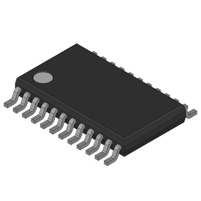
SOIC−24
DW SUFFIX
CASE 751E
1
24
TSSOP−24
DT SUFFIX
CASE 948H
24
HC
4067AG
ALYW
1
1
A
L, WL
Y, YY
W, WW
G
= Assembly Location
= Wafer Lot
= Year
= Work Week
= Pb−Free Package
(Note: Microdot may be in either location)
ORDERING INFORMATION
See detailed ordering and shipping information in the package
dimensions section on page 10 of this data sheet.
© Semiconductor Components Industries, LLC, 2015
May, 2015 − Rev. 2
1
Publication Order Number:
MC74HC4067A/D
�MC74HC4067A
I0
S0
COMMON
INPUT/OUTPUT 1
I7 2
9
10
11
S1
S2 14
S 13
24 VCC
P
N
3
23 I8
I6 3
22 I9
I5 4
21 I10
I4 5
20 I11
I3 6
19 I12
I2 7
18 I13
I1 8
17 I14
I0 9
16 I15
S0 10
15 E
S1 11
14 S2
GND 12
13 S3
BINARY
1 OF 16
DECODER
SN = 5 STAGES
E = 4 STAGES
14 − OUTPUT CIRCUITS
SAME AS ABOVE
(WITH ANALOG INPUTS)
I1 TO I14
1 COMMON
INPUT/
OUTPUT
P
16
15
TOP VIEW
N
I15
E
Figure 1. Pin Assignment
Figure 2. Function Diagram
TRUTH TABLE
S0
S1
S2
S3
E
SELECTED
CHANNEL
X
X
X
X
1
None
0
0
0
0
0
0
1
0
0
0
0
1
0
1
0
0
0
2
1
1
0
0
0
3
0
0
1
0
0
4
1
0
1
0
0
5
0
1
1
0
0
6
1
1
1
0
0
7
0
0
0
1
0
8
1
0
0
1
0
9
0
1
0
1
0
10
1
1
0
1
0
11
0
0
1
1
0
12
1
0
1
1
0
13
0
1
1
1
0
14
1
1
1
1
0
15
H= High Level
L= Low Level
X= Don’t Care
www.onsemi.com
2
�MC74HC4067A
MAXIMUM RATINGS
Symbol
Parameter
Value
Unit
−0.5 to +7.0
V
VCC
DC Supply Voltage
VIS
Analog Input Voltage
−0.5 to VCC + 0.5
V
VIN
Digital Input Voltage
−0.5 to VCC + 0.5
V
IIK
Input Clamping Current
VIN < −0.5 V or VIN > VCC + 0.5 V
±20
mA
ISK
Switch Input Clamping Current
VIS < −0.5 V or VIS > VCC + 0.5 V
±20
mA
IIS
DC Switch Current
±25
mA
IO
DC Output Source / Sink Current
±25
mA
ICC
DC Supply Current per Supply Pin
±100
mA
IGND
DC Ground Current per Ground Pin
±100
mA
TSTG
Storage Temperature Range
−65 to +150
_C
TL
Lead Temperature, 1 mm from Case for 10 Seconds
260
_C
TJ
Junction Temperature under Bias
+150
_C
qJA
Thermal Resistance
SOIC
TSSOP
97
148
_C/W
PD
Power Dissipation in Still Air at 85_C
SOIC
TSSOP
500
450
mW
MSL
Moisture Sensitivity
FR
Flammability Rating
VESD
ILatchup
Level 1
Oxygen Index: 30% − 35%
ESD Withstand Voltage
Human Body Model (Note 1)
Machine Model (Note 2)
Latchup Performance
Above VCC and Below GND at 85_C (Note 3)
UL−94−VO (0.125 in)
>3000
>200
V
±100
mA
Stresses exceeding Maximum Ratings may damage the device. Maximum Ratings are stress ratings only. Functional operation above the
Recommended Operating Conditions is not implied. Extended exposure to stresses above the Recommended Operating Conditions may affect
device reliability.
1. Tested to EIA/JESD22−A114−A.
2. Tested to EIA/JESD22−A115−A.
3. Tested to EIA/JESD78.
RECOMMENDED OPERATING CONDITIONS
Symbol
Parameter
Min
Max
Unit
VCC
Positive DC Supply Voltage (Referenced to GND)
2.0
6.0
V
VIS
Analog Input Voltage (Referenced to GND)
GND
VCC
V
Vin
Digital Input Voltage (Referenced to GND)
GND
VCC
V
VIO*
Static or Dynamic Voltage Across Switch
−
1.2
V
–55
+125
°C
0
0
0
0
1000
600
500
400
ns
TA
Operating Temperature, All Package Types
tr, tf
Input Rise and Fall Rate (Digital Inputs)
VCC = 2.0 V
VCC = 3.0 V
VCC = 4.5 V
VCC = 6.0 V
Functional operation above the stresses listed in the Recommended Operating Ranges is not implied. Extended exposure to stresses beyond
the Recommended Operating Ranges limits may affect device reliability.
*For voltage drops across the switch greater than 1.2 V (switch on), excessive VCC current may be drawn; i.e., the current out of the switch may
contain both VCC and switch input components. The reliability of the device will be unaffected unless the Maximum Ratings are exceeded.
www.onsemi.com
3
�MC74HC4067A
DC ELECTRICAL CHARACTERISTIC Digital Section (Voltages Referenced to GND)
Guaranteed Limit
25°C
VCC
(V)
Min
1.5
2.1
3.15
4.2
Typ
Max
−55 to 125°C
Min
Min
Max
Unit
1.5
2.1
3.15
4.2
V
0.5
0.9
1.35
1.8
0.5
0.9
1.35
1.8
V
±0.1
±1.0
±1.0
mA
4.0
40
80
mA
70
60
160
140
200
175
240
210
W
4.5
6.0
90
80
180
160
225
200
270
240
W
4.5
6.0
10
8.5
Symbol
Parameter
VIH
Minimum High−Level
Input Voltage,
Channel−Select or
Enable Inputs
2.0
3.0
4.5
6.0
VIL
Maximum Low−Level
Input Voltage,
Channel−Select or
Enable Inputs
2.0
3.0
4.5
6.0
0.5
0.9
1.35
1.8
IIN
Input Leakage
Current, Control
Inputs
VIN = VCC or GND
6.0
ICC
Maximum Supply
Current per Package
VIN = VCC or GND, IO=0
VIS = GND or VCC,
VOS = VCC or GND
6.0
RON
ON Resistance
IO = 1 mA
VIN = VCC or GND,
VIS = VCC or GND
4.5
6.0
RON(peak)
ON Resistance
(peak)
IO = 1 mA
VIN = VCC to GND,
VIS = VCC to GND
Conditions
−40 to 85°C
Max
1.5
2.1
3.15
4.2
DRon
ON Resistance
Mismatch Between
Any 2 Switches
IOFF
OFF−State Leakage
Current, All
Channels
SW OFF,
VIS = VCC or GND
6.0
±0.8
±8
±8
mA
ION
ON−State Leakage
Current
SW OFF,
VIS = VCC or GND
6.0
±0.8
±8
±8
mA
www.onsemi.com
4
W
�MC74HC4067A
AC CHARACTERISTICS (INPUT tr, tf = 6 ns)
Guaranteed Limits
25_C
Symbol
tPLH,
tPHL
tON
Parameter
Propagation Delay Switch In to
Out
CL = 50 pF
2.0
4.5
6.0
CL = 15 pF
5.0
CL = 50 pF
2.0
4.5
6.0
CL = 15 pF
5.0
CL = 50 pF
2.0
4.5
6.0
CL = 15 pF
5.0
Min
Typ
–40 to 85_C
Max
Min
Max
–55 to 125_C
Min
Max
Unit
ns
75
15
13
95
19
16
110
22
19
275
55
47
345
69
59
415
83
71
300
60
51
375
75
64
450
90
76
6.0
ns
Switch Turn−ON Time
E to Out
SN to Out
tOFF
Conditions
VCC
(V)
23
25
ns
Switch Turn−OFF Time
E to Out
SN to Out
Cin
Input Capacitance, Control Pins
CPD
Power Dissipation Capacitance
(Note 4)
CL = 50 pF
2.0
4.5
6.0
CL = 15 pF
5.0
CL = 50 pF
2.0
4.5
6.0
CL = 15 pF
5.0
5.0
4. CPD is used to determine the dynamic power consumption, per multivibrator.
www.onsemi.com
5
345
69
59
415
83
71
290
58
49
365
73
62
435
87
74
10
10
10
23
21
3.5
CL = 15 pF
275
55
47
29
pF
pF
�MC74HC4067A
ANALOG SWITCH CHANNEL CHARACTERISTICS
Symbol
Parameter
Conditions
BW
Maximum On−Channel Bandwidth or
Minimum Frequency Response
fin = 1 MHz Sine Wave
Adjust fin Voltage to Obtain 0 dBm at VOS
Increase fin Frequency Until dB Meter Reads – 3 dB
RL = 50 W, CL = 10 pF
Off−Channel Feedthrough Isolation
fin � Sine Wave
Adjust fin Voltage to Obtain 0 dBm at VIS
fin = 10 kHz, RL = 600 W, CL = 50 pF
fin = 1.0 MHz, RL = 50 W, CL = 10 pF
−
−
−
THD
CS
CCOM
Feedthrough Noise
E, Sn to Switch
Crosstalk Between Any Two
Switches
Total Harmonic Distortion
Vin v 1 MHz Square Wave (tr = tf = 6 ns)
Adjust RL at Setup so that IS = 0 A
RL = 600 W, CL = 50 pF
RL = 10 kW, CL = 10 pF
fin � Sine Wave
Adjust fin Voltage to Obtain 0 dBm at VIS
fin = 10 kHz, RL = 600 W, CL = 50 pF
fin = 1.0 MHz, RL = 50 W, CL = 10 pF
fin = 1 kHz, RL = 10 kW, CL = 50 pF
THD = THDMeasured − THDSource
VIS = 4.0 VPP sine wave
VCC
(V)
Limit*
25°C
Unit
4.5
90
MHz
dB
4.5
4.5
−65
−75
mVPP
4.5
4.5
60
30
dB
4.5
4.5
–70
–80
%
4.5
0.04
Switch Input Capacitance
5
pF
Switch Common Capacitance
45
pF
*Limits not tested. Determined by design and verified by qualification.
www.onsemi.com
6
�MC74HC4067A
TYPICAL CHARACTERISTICS
120
80
70
100
125°C
RON @ 4.5 V
80
RON @ 6.0 V
60
125°C
60
25°C
40
50
25°C
40
30
−55°C
20
−55°C
20
10
0
0
0
0.5
1
1.5
2
2.5
3
3.5
VIS, INPUT VOLTAGE (VOLTS),
REFERENCED TO GROUND
4
4.5
0
0
−1
−2
VOS (dB)
−3
−4
−5
−6
−7
VCC = 4.5 V
RL = 50 W
TA = 25°C
−8
−9
−10
100
1000
10000
2
3
4
VIS, INPUT VOLTAGE (VOLTS),
REFERENCED TO GROUND
5
6
Figure 4. Typical On Resistance, VCC = 6.0 V
SWITCH OFF SIGNAL FEEDTHROUGH (dB)
Figure 3. Typical On Resistance, VCC = 4.5 V
1
100000
0
−1
−2
VCC = 4.5 V
RL = 50 W
TA = 25°C
−3
−4
−5
−6
−7
−8
−9
−10
10
100
1000
10000
f, FREQUENCY (kHz)
f, FREQUENCY (kHz)
Figure 5. Typical Switch Frequency Response
Figure 6. Typical Switch OFF Signal
Feedthrough vs Frequency
www.onsemi.com
7
100000
�MC74HC4067A
PLOTTER
PROGRAMMABLE
POWER
SUPPLY
-
MINI COMPUTER
DC ANALYZER
+
VCC
DEVICE
UNDER TEST
ANALOG IN
COMMON OUT
GND
Figure 7. On Resistance Test Setup
VCC
VCC
VCC
VCC
14
GND
14
A
A
VCC
OFF
7
SELECTED
CONTROL
INPUT
N/C
ON
GND
VIL
7
Figure 8. OFF Channel Leakage Current Test
Setup, Any One Channel
SELECTED
CONTROL
INPUT
VIH
Figure 9. ON Channel Leakage Current Test Setup
VCC
14
ANALOG IN
ANALOG OUT
ON
VCC
ANALOG IN
CL*
50%
GND
tPLH
tPHL
7
ANALOG OUT
TEST
POINT
SELECTED
CONTROL
INPUT
VCC
50%
*Includes all probe and jig capacitance.
Figure 10. Propagation Delay, Analog In to Analog
Out
Figure 11. Propagation Delay Test Setup
www.onsemi.com
8
�MC74HC4067A
1
POSITION���WHEN
TESTING tPHZ AND tPZH
2
POSITION��WHEN
TESTING tPLZ AND tPZL
1
tr
2
tf
90%
50%
10%
CONTROL
VCC
VCC
VCC
1 kW
14
1
GND
tPZL
tPLZ
ANALOG
OUT
CL*
HIGH
IMPEDANCE
50%
10%
VOL
90%
VOH
SELECTED
CONTROL
INPUT
tPHZ
tPZH
50%
TEST
POINT
ON/OFF
2
7
HIGH
IMPEDANCE
Figure 12. Turn−ON / Turn−OFF Times
*Includes all probe and jig capacitance.
Figure 13. Turn−ON / Turn−OFF Time Test Setup
VCC
A
VCC
14
N/C
14
fin
N/C
OFF/ON
7
VOS
ON
0.1mF
CL*
SELECTED
CONTROL
INPUT
7
SELECTED
CONTROL
INPUT
dB
METER
VCC
ON/OFF CONTROL
*Includes all probe and jig capacitance.
Figure 14. Power Dissipation Capacitance
Test Setup
Figure 15. ON Channel Bandwidth Test Setup
VCC
VCC/2
VCC
VIS
VOS
14
14
fin
CL*
RL
RL
RL
OFF
0.1mF
VCC/2
OFF/ON
dB
METER
IS
VOS
CL*
SELECTED
CONTROL
INPUT
VCC
GND
7
Vin ≤ 1 MHz
tr = tf = 6 ns
7
SELECTED
CONTROL
INPUT
CONTROL
*Includes all probe and jig capacitance.
*Includes all probe and jig capacitance.
Figure 17. Feedthrough Noise Test Setup
Figure 16. OFF Channel Feedthrough Isolation
Test Setup
www.onsemi.com
9
�MC74HC4067A
VIS
VCC
14
RL
fin
VOS
VIS
ON
VCC
0.1 mF
VOS
0.1 mF
OFF
VCC OR GND
fin
RL
RL
SELECTED
CONTROL
INPUT
VCC/2
CL*
RL
ON
CL*
RL
CL*
TO
DISTORTION
METER
VCC/2
VCC/2
7
7
SELECTED
CONTROL
INPUT
VCC
VCC/2
*Includes all probe and jig capacitance.
*Includes all probe and jig capacitance.
Figure 19. Total Harmonic Distortion Test Setup
Figure 18. Crosstalk Between Any Two Switches
Test Setup
ORDERING INFORMATION
Package
Shipping†
MC74HC4067ADWG
SOIC−24
(Pb−Free)
30 Units / Tube
MC74HC4067ADWR2G
SOIC−24
(Pb−Free)
1000 / Tape & Reel
MC74HC4067ADTG
TSSOP−24
(Pb−Free)
62 Units / Tube
MC74HC4067ADTR2G
TSSOP−24
(Pb−Free)
2500 / Tape & Reel
NLV74HC4067ADTR2G*
TSSOP−24
(Pb−Free)
2500 / Tape & Reel
Device
†For information on tape and reel specifications, including part orientation and tape sizes, please refer to our Tape and Reel Packaging
Specifications Brochure, BRD8011/D.
*NLV Prefix for Automotive and Other Applications Requiring Unique Site and Control Change Requirements; AEC−Q100 Qualified and PPAP
Capable.
www.onsemi.com
10
�MC74HC4067A
PACKAGE DIMENSIONS
SOIC−24 WB
CASE 751E−04
ISSUE F
D
24
E
H
A
B
0.25 C
NOTES:
1. DIMENSIONING AND TOLERANCING PER ASME
Y14.5M, 1994.
2. CONTROLLING DIMENSION: MILLIMETERS.
3. DIMENSIONS b AND c APPLY TO THE FLAT SECTION OF THE LEAD AND ARE MEASURED BETWEEN 0.10 AND 0.25 FROM THE LEAD TIP.
4. DIMENSIONS D AND E1 DO NOT INCLUDE MOLD
FLASH, PROTRUSIONS OR GATE BURRS. MOLD
FLASH, PROTRUSIONS OR GATE BURRS SHALL
NOT EXCEED 0.15 mm PER SIDE. INTERLEAD
FLASH OR PROTRUSION SHALL NOT EXCEED
0.25 PER SIDE. DIMENSIONS D AND E1 ARE
DETERMINED AT DATUM H.
5. A1 IS DEFINED AS THE VERTICAL DISTANCE
FROM THE SEATING PLANE TO THE LOWEST
POINT ON THE PACKAGE BODY.
13
E1
1
L
12
C
DETAIL A
24X b
PIN 1
INDICATOR
0.25
TOP VIEW
M
C A
S
B
S
h
x 45 _
A
A1
e
NOTE 5
DIM
A
A1
b
c
D
E
E1
e
h
L
M
NOTE 3
C
M
c
SEATING
PLANE
NOTE 3
DETAIL A
END VIEW
SIDE VIEW
RECOMMENDED
SOLDERING FOOTPRINT*
24X
24X
1.62
0.52
11.00
1
1.27
PITCH
DIMENSIONS: MILLIMETERS
*For additional information on our Pb−Free strategy and soldering
details, please download the ON Semiconductor Soldering and
Mounting Techniques Reference Manual, SOLDERRM/D.
www.onsemi.com
11
MILLIMETERS
MIN
MAX
2.35
2.65
0.13
0.29
0.35
0.49
0.23
0.32
15.25
15.54
10.30 BSC
7.40
7.60
1.27 BSC
0.25
0.75
0.41
0.90
0_
8_
�MC74HC4067A
PACKAGE DIMENSIONS
TSSOP24 7.8x4.4, 0.65P
CASE 948H
ISSUE B
NOTE 4
NOTE 6
B
NOTE 5
A
D
NOTE 6
24
L2
13
GAUGE
PLANE
E1
L
E
C
DETAIL A
PIN 1
1
REFERENCE
12
e
24X
TOP VIEW
0.15 C B
b
0.10
C B
M
S
SIDE VIEW
S
H
A1
0.10 C
24X
A
NOTE 3
A
0.05 C
S
2X 12 TIPS
C
SEATING
PLANE
DETAIL A
c
END VIEW
M
NOTES:
1. DIMENSIONING AND TOLERANCING PER ASME Y14.5M,
1994.
2. CONTROLLING DIMENSION: MILLIMETERS.
3. DIMENSION b DOES NOT INCLUDE DAMBAR PROTRUSION.
DAMBAR PROTRUSION SHALL BE 0.08 MAX AT MMC. DAMBAR
CANNOT BE LOCATED ON THE LOWER RADIUS OF THE FOOT.
4. DIMENSION D DOES NOT INCLUDE MOLD FLASH,
PROTRUSIONS OR GATE BURRS. MOLD FLASH,
PROTRUSIONS OR GATE BURRS SHALL NOT EXCEED 0.15
PER SIDE. DIMENSION D IS DETERMINED AT DATUM PLANE H.
5. DIMENSION E1 DOES NOT INCLUDE INTERLEAD FLASH OR
PROTRUSION. INTERLEAD FLASH OR PROTRUSION SHALL
NOT EXCEED 0.25 PER SIDE. DIMENSION E1 IS DETERMINED
AT DATUM PLANE H.
6. DATUMS A AND B ARE DETERMINED AT DATUM PLANE H.
7. A1 IS DEFINED AS THE VERTICAL DISTANCE FROM THE
SEATING PLANE TO THE LOWEST POINT ON THE PACKAGE
BODY. MILLIMETERS
DIM MIN
MAX
A
1.20
--A1
0.05
0.15
b
0.19
0.30
c
0.09
0.20
D
7.90
7.70
E
6.40 BSC
E1
4.30
4.50
e
0.65 BSC
L
0.50
0.75
L2
0.25 BSC
M
0_
8_
RECOMMENDED
SOLDERING FOOTPRINT
24X
0.42
24X
1.15
6.70
0.65
PITCH
DIMENSIONS: MILLIMETERS
ON Semiconductor and the
are registered trademarks of Semiconductor Components Industries, LLC (SCILLC) or its subsidiaries in the United States and/or other countries.
SCILLC owns the rights to a number of patents, trademarks, copyrights, trade secrets, and other intellectual property. A listing of SCILLC’s product/patent coverage may be accessed
at www.onsemi.com/site/pdf/Patent−Marking.pdf. SCILLC reserves the right to make changes without further notice to any products herein. SCILLC makes no warranty, representation
or guarantee regarding the suitability of its products for any particular purpose, nor does SCILLC assume any liability arising out of the application or use of any product or circuit, and
specifically disclaims any and all liability, including without limitation special, consequential or incidental damages. “Typical” parameters which may be provided in SCILLC data sheets
and/or specifications can and do vary in different applications and actual performance may vary over time. All operating parameters, including “Typicals” must be validated for each
customer application by customer’s technical experts. SCILLC does not convey any license under its patent rights nor the rights of others. SCILLC products are not designed, intended,
or authorized for use as components in systems intended for surgical implant into the body, or other applications intended to support or sustain life, or for any other application in which
the failure of the SCILLC product could create a situation where personal injury or death may occur. Should Buyer purchase or use SCILLC products for any such unintended or
unauthorized application, Buyer shall indemnify and hold SCILLC and its officers, employees, subsidiaries, affiliates, and distributors harmless against all claims, costs, damages, and
expenses, and reasonable attorney fees arising out of, directly or indirectly, any claim of personal injury or death associated with such unintended or unauthorized use, even if such claim
alleges that SCILLC was negligent regarding the design or manufacture of the part. SCILLC is an Equal Opportunity/Affirmative Action Employer. This literature is subject to all applicable
copyright laws and is not for resale in any manner.
PUBLICATION ORDERING INFORMATION
LITERATURE FULFILLMENT:
Literature Distribution Center for ON Semiconductor
P.O. Box 5163, Denver, Colorado 80217 USA
Phone: 303−675−2175 or 800−344−3860 Toll Free USA/Canada
Fax: 303−675−2176 or 800−344−3867 Toll Free USA/Canada
Email: orderlit@onsemi.com
N. American Technical Support: 800−282−9855 Toll Free
USA/Canada
Europe, Middle East and Africa Technical Support:
Phone: 421 33 790 2910
Japan Customer Focus Center
Phone: 81−3−5817−1050
www.onsemi.com
12
ON Semiconductor Website: www.onsemi.com
Order Literature: http://www.onsemi.com/orderlit
For additional information, please contact your local
Sales Representative
MC74HC4067A/D
�


 工商网监
湘ICP备2023018690号
工商网监
湘ICP备2023018690号
