NCP2823AGEVB,
NCP2823BGEVB
NCP2823 Series Evaluation
Board User's Manual
http://onsemi.com
EVAL BOARD USER’S MANUAL
Overview
The NCP2823A/B are cost effective mono audio power
amplifiers designed for portable electronic devices.
NCP2823A is optimized for 8 W operation and NCP2823B
can operate with speaker impedance down to 4.0 W. For
Instance, NCP2823B is capable of delivering 3 W of
continuous average power to a 4.0 W from a 5.0 V supply in
a Bridge Tied Load (BTL) configuration. Under the same
conditions, NCP2823A can provide 1.5 W to an 8.0 W BTL
load with less than 1% THD+N. For cellular handsets or
PDAs it offers space and cost savings because no output
filter is required when using inductive transducers. With
more than 95% efficiency and very low shutdown current,
it increases the lifetime of your battery and drastically
lowers the junction temperature.
The intent of the evaluation boards is to illustrate typical
operation of the NCP2823 device for laboratory
characterization. The NCP2823 Series Evaluation Board
schematic is depicted in Figure 3.
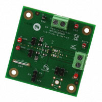
Figure 1. NCP2823AGEVB Board Picture
© Semiconductor Components Industries, LLC, 2012
April, 2012 − Rev. 2
Figure 2. NCP2823BGEVB Board Picture
1
Publication Order Number:
EVBUM2108/D
�NCP2823AGEVB, NCP2823BGEVB
BOARD SCHEMATIC
J 30
FILTER
VD D
C3
J5
150k
EN
C2
1
J 10
J 31
100n
C2
R2
C1
150k
B2
1
100n
A1
INP
OU TP
out p
A3
1
L1
2
NM
C9
out pf
NM
INM
A2
1
2
OU TM
C3
out n
1
J 17
L2
out nf
2
NM
C8
NM
N C P2823
0
PROBE CONNECTION
2
1
1
1
2
J7
POWER SUPPLY
0
J2
out n
J6
J 13
0
2
1
1
J4
GN D
1
2
C7
100uF
J1
1
2
3
2
1
J 25
ENABLE
1
2
out p
J 32
VD D
J 11
SPEAKER
CONNECTION
2
1
0
EN
PGN D
R1
B3
J9
C1
PVD D
U1
1
B1
2
1
J8
J 12
0
NM
AVD D
BOARD FIXATION HOLES
1
2
0
4. 7uF
C4
AGN D
0
1
2
1
J 29
1
J 28
1
1
J 27
J 20
1
2
3
4
5
VD D
J 26
EN
0
1
0
J3
0
Tit le
Size
A
D ate:
N C P2823EVB
D oc um ent N um ber
N C P2823EVB TLS−P−001−A−1109−R D
Thurs day , J anuary 07, 2010
Sheet
R ev
A
1
of
1
Figure 3. NCP2823 Series Evaluation Board Schematic
OPERATION
Performances of EVB Solution
The operating power supply of the NCP2823 is from 2.5
to 5.5 V. The absolute maximum input voltage is 7.0 V. A
power supply set to 3.6 V and current limit set to at least
1.5 A must be connected to J11 connector to powering the
NCP2823 Series Evaluation Board. Also to compensate for
parasitic inductance of wires between the power supply and
the evaluation board it is highly recommended to connect a
470 mF electrolytic capacitor to bypass J11 terminal. Like
this the device can be evaluate under powering condition
very similar that battery power supplies.
To be as close as possible with final handset application,
the design of this power conversion solution used small size
footprints where possible. Changing components may
positively or negatively impact the evaluation board
performance, illustrated in Figure 4 to 9. For more
information please refer to the NCP2823 datasheet.
http://onsemi.com
2
�NCP2823AGEVB, NCP2823BGEVB
Table 1. BOARD CONNECTIONS
INPUT POWER
Symbol
Descriptions
J11−1
This is the positive connection for power supply. The leads (positive + ground) to the input supply should
be twisted and kept as short as possible.
J11−2
This is the return connection for the power supply (Ground signal)
J4
Ground clip
AUDIO
Descriptions
Symbol
J9
Positive Audio input
J10
Negative Audio input
J17−2
Positive Audio output
J17−1
Negative Audio output
SWITCHES SETUP
Switch Descriptions
Symbol
J1
Enable
J5
Short input capacitor on positive input
J6
Short input capacitor on negative input
J7
Connect the positive audio input to Gnd
J8
Connect the negative audio input to Gnd
J31
Short filter on positive output
J32
Short filter on negative output
J25
Connect negative output to Probe connection (J26)
J20
Connect Positive output to Probe connection (J26)
TEST POINT
Switch Descriptions
Symbol
J3
This test point is directly connected to the GND
J2
This test point is directly connected to the Vdd pin
J9
This test point is connected to the positive audio input
J10
This test point is connected to the negative audio input
J12
This test point is connected to the positive audio output
J13
This test point is connected to the negative audio output
J26
Probe connection
http://onsemi.com
3
�NCP2823AGEVB, NCP2823BGEVB
TYPICAL OPERATING CHARACTERISTICS
THD+ N vs Pout @ 255C
V p=2.5V
V p=2.7V
V p=3V
V p=3.6V
THD+ N vs Pout @ 255C
V p=4.2V
V p=5V
V p=2.5V
V p=5.5V
V p=3V
V p=3.6V
V p=4.2V
V p=5V
V p=5.5V
100
100
10
THD (% )
10
THD (%)
V p=2.7V
1
1
0.1
0.1
0.01
10
100
1000
0.01
10000
10
100
Pout (mW)
Figure 4. THD vs. POUT, RI = 8 W, f = 1 kHz
V p=2.7V
V p=3V
V p=3.6V
10000
Figure 5. THD vs. POUT, RI = 4 W, f = 1 kHz
Effi ci e ncy vs vs Pout @ 255C
V p=2.5V
1000
Pout (mW)
THD vs Fre que ncy @ Pout= 250mW
V p=4.2V
V p=5V
V p=5V
V p=5.5V
V p=3.6V
V p=2.5V
1
100
90
80
70
0.1
THD(%)
(% )
60
50
40
0.01
30
20
10
0.001
0
0
500
1000
1500
10
2000
100
1000
10000
100000
Fr eq( Hz )
Pout (mW)
Figure 6. Efficiency vs. POUT, RI = 8 W, f = 1 kHz
Figure 7. THD vs. Frequency, RI = 8 W,
POUT = 250 mW
THD vs Fre que ncy @ Pout= 1W
PSRR vs. Fre q I nput gnd (100nF)
V p=5V
0
1
− 10
− 20
V p=2.5V
V p=3.6V
− 30
THD(% )
PSRR (dB)
0.1
V p=4.2V
− 40
− 50
− 60
0.01
− 70
− 80
− 90
0.001
10
100
1000
10000
10
100000
100
1000
10000
f r eq ( Hz)
Fr eq( Hz )
Figure 9. PSRR vs. Frequency
Figure 8. THD vs. Frequency, RI = 8 W, POUT = 1 W
http://onsemi.com
4
100000
�NCP2823AGEVB, NCP2823BGEVB
PCB LAYOUT
As with all Class D amplifier, care must has been observed
to place the components on the PCB and layout the critical
nodes. The evaluation board is made of 4 PCB layers where
first internal layer is a GND. Figure 10, Figure 12 and
Figure 13 show the layout of the NCP2823 Series evaluation
board. For more specific layout guidelines please refer to the
NCP2823 datasheet.
Figure 10. Assembly Layer TOP
Figure 11. Assembly Layer BOTTOM
http://onsemi.com
5
�NCP2823AGEVB, NCP2823BGEVB
Figure 12. Top Layer Routing
Figure 13. Bottom Layer Routing
http://onsemi.com
6
�NCP2823AGEVB, NCP2823BGEVB
Table 2. BILL OF MATERIALS
Qty
Ref Des.
Description
Size
Manufacturer
Part Number
1
U1
NCP2823
CSP−9
1.45 x 1.45
mm
ON Semiconductor
NCP2823
2
C1, C2
Capacitor, Ceramic 100 nF
0603
KEMET
C0603C104K5RAC
2
C4
Capacitor, Ceramic 4.7 mF 6.3 V
0603
KEMET
C0603C475K9PAC
2
R1, R2
Resistor 150k 1%
0603
Std
Any supplier possible
2
J11,
J17
Mal. SL5.08/2/90B plus Fem. BLZ
5.08/2
Weidmuller
SL5.08/2/90 +
BLZ 5.08/2
3
J1
Header 3 pin, 100 mil spacing
0.100 x 2
Std
Std
2
J7, J8
Header 2 pin, 100 mil spacing
0.100 x 2
Std
Std
1
J7
GND Connection
Std
Std
9
J2, J3, J9,
J10, J12, J13
Test Point
Std
Std
2
J31, J32
Soldering point must be connected
1
PCB
PCB 2.0 in x 2.0 in x 1.0 mm, 4 Layers
Any
TLS−P−001−A−1109−RD
NOTE: Component J20, J25, J26, L1, L2, C8 and C9 are not mounted on this demokit.
ASSEMBLY TEST PROCEDURE
Wake up test
A power supply set to 3.6 V and current limit set to at least
1.5 A must be connected to J15 connector to powering the
NCP2823 Series evaluation board. Also to compensate for
parasitic inductance of wires between the power supply and
the evaluation board it is highly recommended to connect a
470 mF electrolytic capacitor to bypass J11 terminal. Like
this the device can be evaluate under powering condition
very similar that battery power supplies.
These tests are provided in order to guarantee a good
assembly of the NCP2823 on its dedicated board, it do not
consist in parametric test which is already done at chip level.
Switches setup for wire mode test:
Symbol
J1
Tests:
4. Set the switches in the configuration
5. Power the board with a 3.6 V power supply
limited at 1.5 A and bypassed by a 470 mF
electrolytic capacitor.
6. Measure DC Output voltage on J12 on J13 and
GND. DC Voltage must be equal to 1.8 V
7. Measure DC input voltage on J5−2 on J6−2 and
GND. DC Voltage must be equal to 1.26 V
Switches setup for shutdown test:
J1
Must be connected to VDD (high side)
*All other switches must be kept floating
SHUTDOWN TEST
Symbol
Switch Description
Switch Description
Must be connected to ground (low side)
SUMMARY
*All other switches must be kept floating
Tests:
1. Set the switches in the configuration
2. Power the board with a 3.6 V power supply
limited at 1.5A and bypassed by a 470 mF
electrolytic capacitor.
3. Measure the current on the power supply (must be
inferior to 1 mA)
Test
Measurement
Shutdown test
I Supply
Wake up test
VOUTP, VOUTN
VJ9, VJ10
Switch Description
I < 1 mA
VDC = 1.8 V
VDC = 1.26 V
NOTE: For each board a Test Result Table must be fully
completed (see the next page)
http://onsemi.com
7
�NCP2823AGEVB, NCP2823BGEVB
TEST RESULT TABLE
NCP2823 Assembly Test
Date
Operator Name
Board Serial Number
Test No.
Test Name
Results
1
Shutdown mode test
I Supply
2
Wake up test
VoutP, VoutN
1.8
VJ9, VJ10
1.26
http://onsemi.com
8
Value
�onsemi,
, and other names, marks, and brands are registered and/or common law trademarks of Semiconductor Components Industries, LLC dba “onsemi” or its affiliates
and/or subsidiaries in the United States and/or other countries. onsemi owns the rights to a number of patents, trademarks, copyrights, trade secrets, and other intellectual property. A
listing of onsemi’s product/patent coverage may be accessed at www.onsemi.com/site/pdf/Patent−Marking.pdf. onsemi is an Equal Opportunity/Affirmative Action Employer. This
literature is subject to all applicable copyright laws and is not for resale in any manner.
The evaluation board/kit (research and development board/kit) (hereinafter the “board”) is not a finished product and is not available for sale to consumers. The board is only intended
for research, development, demonstration and evaluation purposes and will only be used in laboratory/development areas by persons with an engineering/technical training and familiar
with the risks associated with handling electrical/mechanical components, systems and subsystems. This person assumes full responsibility/liability for proper and safe handling. Any
other use, resale or redistribution for any other purpose is strictly prohibited.
THE BOARD IS PROVIDED BY ONSEMI TO YOU “AS IS” AND WITHOUT ANY REPRESENTATIONS OR WARRANTIES WHATSOEVER. WITHOUT LIMITING THE FOREGOING,
ONSEMI (AND ITS LICENSORS/SUPPLIERS) HEREBY DISCLAIMS ANY AND ALL REPRESENTATIONS AND WARRANTIES IN RELATION TO THE BOARD, ANY
MODIFICATIONS, OR THIS AGREEMENT, WHETHER EXPRESS, IMPLIED, STATUTORY OR OTHERWISE, INCLUDING WITHOUT LIMITATION ANY AND ALL
REPRESENTATIONS AND WARRANTIES OF MERCHANTABILITY, FITNESS FOR A PARTICULAR PURPOSE, TITLE, NON−INFRINGEMENT, AND THOSE ARISING FROM A
COURSE OF DEALING, TRADE USAGE, TRADE CUSTOM OR TRADE PRACTICE.
onsemi reserves the right to make changes without further notice to any board.
You are responsible for determining whether the board will be suitable for your intended use or application or will achieve your intended results. Prior to using or distributing any systems
that have been evaluated, designed or tested using the board, you agree to test and validate your design to confirm the functionality for your application. Any technical, applications or
design information or advice, quality characterization, reliability data or other services provided by onsemi shall not constitute any representation or warranty by onsemi, and no additional
obligations or liabilities shall arise from onsemi having provided such information or services.
onsemi products including the boards are not designed, intended, or authorized for use in life support systems, or any FDA Class 3 medical devices or medical devices with a similar
or equivalent classification in a foreign jurisdiction, or any devices intended for implantation in the human body. You agree to indemnify, defend and hold harmless onsemi, its directors,
officers, employees, representatives, agents, subsidiaries, affiliates, distributors, and assigns, against any and all liabilities, losses, costs, damages, judgments, and expenses, arising
out of any claim, demand, investigation, lawsuit, regulatory action or cause of action arising out of or associated with any unauthorized use, even if such claim alleges that onsemi was
negligent regarding the design or manufacture of any products and/or the board.
This evaluation board/kit does not fall within the scope of the European Union directives regarding electromagnetic compatibility, restricted substances (RoHS), recycling (WEEE), FCC,
CE or UL, and may not meet the technical requirements of these or other related directives.
FCC WARNING – This evaluation board/kit is intended for use for engineering development, demonstration, or evaluation purposes only and is not considered by onsemi to be a finished
end product fit for general consumer use. It may generate, use, or radiate radio frequency energy and has not been tested for compliance with the limits of computing devices pursuant
to part 15 of FCC rules, which are designed to provide reasonable protection against radio frequency interference. Operation of this equipment may cause interference with radio
communications, in which case the user shall be responsible, at its expense, to take whatever measures may be required to correct this interference.
onsemi does not convey any license under its patent rights nor the rights of others.
LIMITATIONS OF LIABILITY: onsemi shall not be liable for any special, consequential, incidental, indirect or punitive damages, including, but not limited to the costs of requalification,
delay, loss of profits or goodwill, arising out of or in connection with the board, even if onsemi is advised of the possibility of such damages. In no event shall onsemi’s aggregate liability
from any obligation arising out of or in connection with the board, under any theory of liability, exceed the purchase price paid for the board, if any.
The board is provided to you subject to the license and other terms per onsemi’s standard terms and conditions of sale. For more information and documentation, please visit
www.onsemi.com.
PUBLICATION ORDERING INFORMATION
LITERATURE FULFILLMENT:
Email Requests to: orderlit@onsemi.com
onsemi Website: www.onsemi.com
◊
TECHNICAL SUPPORT
North American Technical Support:
Voice Mail: 1 800−282−9855 Toll Free USA/Canada
Phone: 011 421 33 790 2910
www.onsemi.com
1
Europe, Middle East and Africa Technical Support:
Phone: 00421 33 790 2910
For additional information, please contact your local Sales Representative
�


 工商网监
湘ICP备2023018690号
工商网监
湘ICP备2023018690号
