DATA SHEET
www.onsemi.com
PNP Silicon Planar
Epitaxial Transistor
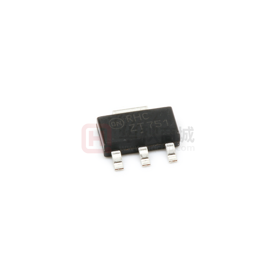
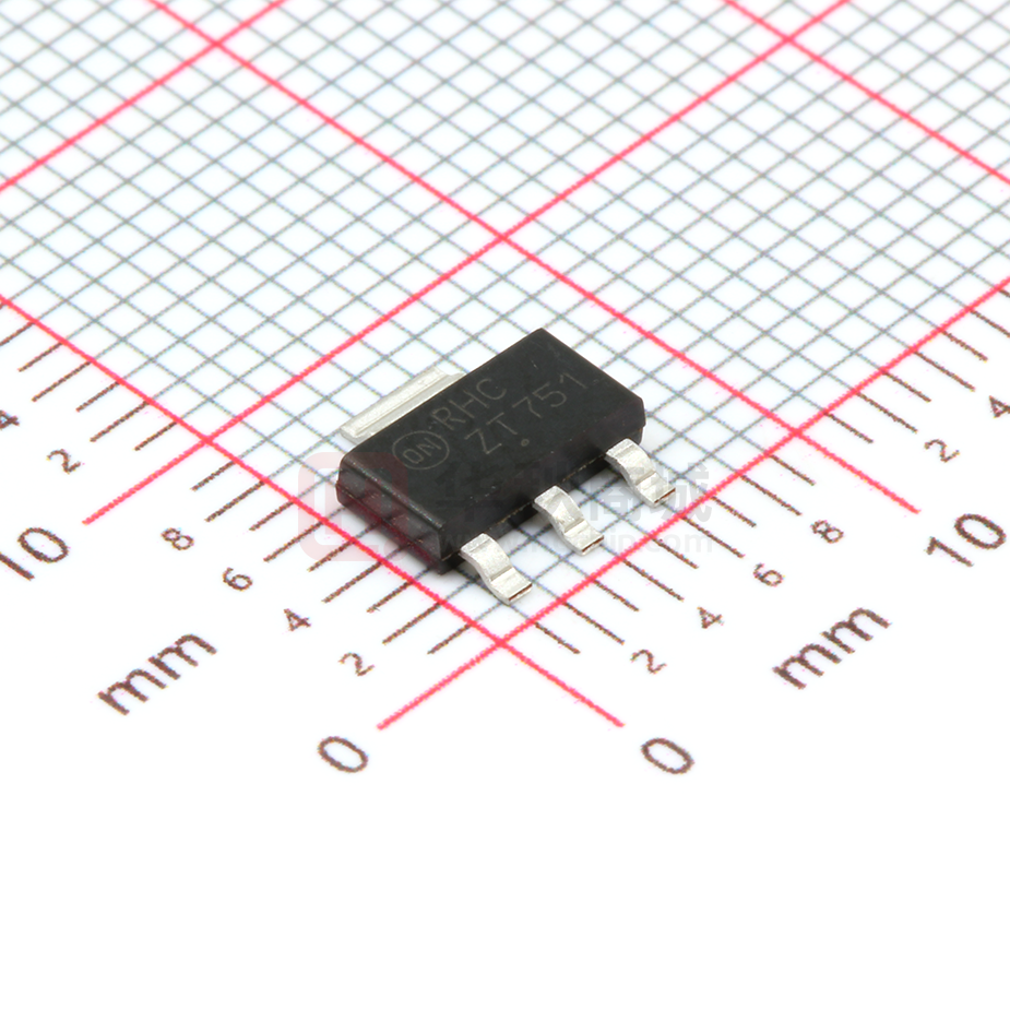
PZT751T1
SOT−223 PACKAGE HIGH CURRENT
NPN SILICON TRANSISTOR
SURFACE MOUNT
This PNP Silicon Epitaxial transistor is designed for use in
industrial and consumer applications. The device is housed in the
SOT−223 package which is designed for medium power surface
mount applications.
4
1
Features
• High Current
• The SOT−223 Package can be soldered using wave or reflow.
• SOT−223 Package Ensures Level Mounting, Resulting in
•
•
•
BASE
1
EMITTER 3
MARKING DIAGRAM
MAXIMUM RATINGS (TC = 25°C unless otherwise noted)
1
Symbol
Value
Unit
Collector−Emitter Voltage
VCEO
−60
Vdc
Collector−Base Voltage
VCBO
−80
Vdc
Emitter−Base Voltage
VEBO
−5.0
Vdc
Collector Current
IC
−2.0
Adc
Total Power Dissipation
@ TA = 25°C (Note 1)
Derate above 25°C
PD
Storage Temperature Range
Tstg
−65 to 150
°C
Junction Temperature
TJ
150
°C
0.8
6.4
W
mW/°C
THERMAL CHARACTERISTICS
Rating
Thermal Resistance from Junction−to−
Ambient in Free Air
Maximum Temperature for Soldering
Purposes
Time in Solder Bath
A
Y
W
G
Symbol
Value
Unit
RqJA
156
°C/W
TL
260
°C
10
Sec
AYW
ZT751G
G
= Assembly Location
= Year
= Work Week
= Pb−Free Package
(Note: Microdot may be in either location)
ORDERING INFORMATION
Device
Stresses exceeding those listed in the Maximum Ratings table may damage the
device. If any of these limits are exceeded, device functionality should not be
assumed, damage may occur and reliability may be affected.
1. Device mounted on a FR−4 glass epoxy printed circuit board using minimum
recommended footprint.
3
COLLECTOR 2, 4
Improved Thermal Conduction, and Allows Visual Inspection of
Soldered Joints. The Formed Leads Absorb Thermal Stress During
Soldering, Eliminating the Possibility of Damage to the Die
NPN Complement is PZT651T1G
S Prefix for Automotive and Other Applications Requiring Unique
Site and Control Change Requirements; AEC−Q101 Qualified and
PPAP Capable
These Devices are Pb−Free, Halogen Free/BFR Free and are RoHS
Compliant*
Rating
2
SOT−223
CASE 318E
STYLE 1
Package
Shipping†
PZT751T1G
SOT−223
(Pb−Free)
1,000 / Tape & Reel
SPZT751T1G
SOT−223
(Pb−Free)
1,000 / Tape & Reel
†For information on tape and reel specifications,
including part orientation and tape sizes, please
refer to our Tape and Reel Packaging Specifications
Brochure, BRD8011/D.
*For additional information on our Pb−Free strategy and soldering details, please
download the onsemi Soldering and Mounting Techniques Reference Manual,
SOLDERRM/D.
© Semiconductor Components Industries, LLC, 2015
June, 2022 − Rev. 10
1
Publication Order Number:
PZT751T1/D
�PZT751T1
ELECTRICAL CHARACTERISTICS (TA = 25°C unless otherwise noted)
Characteristics
Symbol
Min
Max
−60
−
−80
−
−5.0
−
−
−0.1
−
−100
75
75
75
40
−
−
−
−
−
−
−0.5
−0.3
−
−1.0
−
−1.2
75
−
Unit
OFF CHARACTERISTICS
Collector−Emitter Breakdown Voltage
(IC = −10 mAdc, IB = 0)
V(BR)CEO
Collector−Emitter Breakdown Voltage
(IC = −100 mAdc, IE = 0)
V(BR)CBO
Emitter−Base Breakdown Voltage
(IE = −10 mAdc, IC = 0)
V(BR)EBO
Base−Emitter Cutoff Current
(VEB = −4.0 Vdc)
IEBO
Collector−Base Cutoff Current
(VCB = −80 Vdc, IE = 0)
ICBO
Vdc
Vdc
Vdc
mAdc
nAdc
ON CHARACTERISTICS (Note 2)
DC Current Gain
(IC = −50 mAdc, VCE = −2.0 Vdc)
(IC = −500 mAdc, VCE = −2.0 Vdc)
(IC = −1.0 Adc, VCE = −2.0 Vdc)
(IC = −2.0 Adc, VCE = −2.0 Vdc)
hFE
Collector−Emitter Saturation Voltages
(IC = −2.0 Adc, IB = −200 mAdc)
(IC = −1.0 Adc, IB = −100 mAdc)
VCE(sat)
Base−Emitter Voltages
(IC = −1.0 Adc, VCE = −2.0 Vdc)
VBE(on)
Base−Emitter Saturation Voltage
(IC = −1.0 Adc, IB = −100 mAdc)
VBE(sat)
Current−Gain−Bandwidth
(IC = −50 mAdc, VCE = −5.0 Vdc, f = 100 MHz)
fT
2. Pulse Test: Pulse Width ≤ 300 ms, Duty Cycle = 2.0%.
www.onsemi.com
2
−
Vdc
Vdc
Vdc
MHz
�PZT751T1
TYPICAL CHARACTERISTICS
250
225
-2.0
TJ = 125°C
-1.8
VCE = -2.0 V
-1.6
V, VOLTAGE (VOLTS)
hFE, DC CURRENT GAIN
200
175
150
25°C
125
100
-�55°C
75
-1.4
-1.2
-0.8
VBE(on) @ VCE = 2.0 V
-0.6
50
-0.4
25
-0.2
0
-10 -�20
VBE(sat) @ IC/IB = 10
-1.0
VCE(sat) @ IC/IB = 10
0
-50
-�50 -100 -�200 -�500 -1.0 A -2.0 A -4.0 A
IC, COLLECTOR CURRENT (mA)
10
-1.0
-0.9
TJ = 25°C
-0.8
-0.7
-0.6
-0.5
-0.4
IC = -500 mA
-0.3
IC = -2.0 A
-0.2
IC = -10 mA
IC = -100 mA
0
-0.05 -0.1 -0.2 -0.5 -1.0 -2.0 -5.0 -10 -20
IB, BASE CURRENT (mA)
IC, COLLECTOR CURRENT (A)
VCE , COLLECTOR-EMITTER VOLTAGE (VOLTS)
-200
-500 -1.0 A
IC, COLLECTOR CURRENT (mA)
-2.0 A
-4.0 A
Figure 2. On Voltages
Figure 1. Typical DC Current Gain
-0.1
-100
100 ms
1 ms
1
10 ms
100 ms
0.1
1s
0.01
0.001
-50 -100-200 -500
10 ms, 1 ms
Single Pulse Test @ TA = 25°C
0.01
0.1
1
10
VCE, COLLECTOR−EMITTER VOLTAGE (V)
Figure 3. Collector Saturation Region
Figure 4. Safe Operating Area
www.onsemi.com
3
100
�MECHANICAL CASE OUTLINE
PACKAGE DIMENSIONS
SOT−223 (TO−261)
CASE 318E−04
ISSUE R
DATE 02 OCT 2018
SCALE 1:1
q
q
DOCUMENT NUMBER:
DESCRIPTION:
98ASB42680B
SOT−223 (TO−261)
Electronic versions are uncontrolled except when accessed directly from the Document Repository.
Printed versions are uncontrolled except when stamped “CONTROLLED COPY” in red.
PAGE 1 OF 2
ON Semiconductor and
are trademarks of Semiconductor Components Industries, LLC dba ON Semiconductor or its subsidiaries in the United States and/or other countries.
ON Semiconductor reserves the right to make changes without further notice to any products herein. ON Semiconductor makes no warranty, representation or guarantee regarding
the suitability of its products for any particular purpose, nor does ON Semiconductor assume any liability arising out of the application or use of any product or circuit, and specifically
disclaims any and all liability, including without limitation special, consequential or incidental damages. ON Semiconductor does not convey any license under its patent rights nor the
rights of others.
© Semiconductor Components Industries, LLC, 2018
www.onsemi.com
�SOT−223 (TO−261)
CASE 318E−04
ISSUE R
STYLE 1:
PIN 1.
2.
3.
4.
BASE
COLLECTOR
EMITTER
COLLECTOR
STYLE 2:
PIN 1.
2.
3.
4.
ANODE
CATHODE
NC
CATHODE
STYLE 6:
PIN 1.
2.
3.
4.
RETURN
INPUT
OUTPUT
INPUT
STYLE 7:
PIN 1.
2.
3.
4.
ANODE 1
CATHODE
ANODE 2
CATHODE
STYLE 11:
PIN 1. MT 1
2. MT 2
3. GATE
4. MT 2
STYLE 3:
PIN 1.
2.
3.
4.
GATE
DRAIN
SOURCE
DRAIN
STYLE 8:
STYLE 12:
PIN 1. INPUT
2. OUTPUT
3. NC
4. OUTPUT
CANCELLED
DATE 02 OCT 2018
STYLE 4:
PIN 1.
2.
3.
4.
SOURCE
DRAIN
GATE
DRAIN
STYLE 5:
PIN 1.
2.
3.
4.
STYLE 9:
PIN 1.
2.
3.
4.
INPUT
GROUND
LOGIC
GROUND
STYLE 10:
PIN 1. CATHODE
2. ANODE
3. GATE
4. ANODE
DRAIN
GATE
SOURCE
GATE
STYLE 13:
PIN 1. GATE
2. COLLECTOR
3. EMITTER
4. COLLECTOR
GENERIC
MARKING DIAGRAM*
AYW
XXXXXG
G
1
A
= Assembly Location
Y
= Year
W
= Work Week
XXXXX = Specific Device Code
G
= Pb−Free Package
(Note: Microdot may be in either location)
*This information is generic. Please refer to
device data sheet for actual part marking.
Pb−Free indicator, “G” or microdot “G”, may
or may not be present. Some products may
not follow the Generic Marking.
DOCUMENT NUMBER:
DESCRIPTION:
98ASB42680B
SOT−223 (TO−261)
Electronic versions are uncontrolled except when accessed directly from the Document Repository.
Printed versions are uncontrolled except when stamped “CONTROLLED COPY” in red.
PAGE 2 OF 2
ON Semiconductor and
are trademarks of Semiconductor Components Industries, LLC dba ON Semiconductor or its subsidiaries in the United States and/or other countries.
ON Semiconductor reserves the right to make changes without further notice to any products herein. ON Semiconductor makes no warranty, representation or guarantee regarding
the suitability of its products for any particular purpose, nor does ON Semiconductor assume any liability arising out of the application or use of any product or circuit, and specifically
disclaims any and all liability, including without limitation special, consequential or incidental damages. ON Semiconductor does not convey any license under its patent rights nor the
rights of others.
© Semiconductor Components Industries, LLC, 2018
www.onsemi.com
�onsemi,
, and other names, marks, and brands are registered and/or common law trademarks of Semiconductor Components Industries, LLC dba “onsemi” or its affiliates
and/or subsidiaries in the United States and/or other countries. onsemi owns the rights to a number of patents, trademarks, copyrights, trade secrets, and other intellectual property.
A listing of onsemi’s product/patent coverage may be accessed at www.onsemi.com/site/pdf/Patent−Marking.pdf. onsemi reserves the right to make changes at any time to any
products or information herein, without notice. The information herein is provided “as−is” and onsemi makes no warranty, representation or guarantee regarding the accuracy of the
information, product features, availability, functionality, or suitability of its products for any particular purpose, nor does onsemi assume any liability arising out of the application or use
of any product or circuit, and specifically disclaims any and all liability, including without limitation special, consequential or incidental damages. Buyer is responsible for its products
and applications using onsemi products, including compliance with all laws, regulations and safety requirements or standards, regardless of any support or applications information
provided by onsemi. “Typical” parameters which may be provided in onsemi data sheets and/or specifications can and do vary in different applications and actual performance may
vary over time. All operating parameters, including “Typicals” must be validated for each customer application by customer’s technical experts. onsemi does not convey any license
under any of its intellectual property rights nor the rights of others. onsemi products are not designed, intended, or authorized for use as a critical component in life support systems
or any FDA Class 3 medical devices or medical devices with a same or similar classification in a foreign jurisdiction or any devices intended for implantation in the human body. Should
Buyer purchase or use onsemi products for any such unintended or unauthorized application, Buyer shall indemnify and hold onsemi and its officers, employees, subsidiaries, affiliates,
and distributors harmless against all claims, costs, damages, and expenses, and reasonable attorney fees arising out of, directly or indirectly, any claim of personal injury or death
associated with such unintended or unauthorized use, even if such claim alleges that onsemi was negligent regarding the design or manufacture of the part. onsemi is an Equal
Opportunity/Affirmative Action Employer. This literature is subject to all applicable copyright laws and is not for resale in any manner.
PUBLICATION ORDERING INFORMATION
LITERATURE FULFILLMENT:
Email Requests to: orderlit@onsemi.com
onsemi Website: www.onsemi.com
◊
TECHNICAL SUPPORT
North American Technical Support:
Voice Mail: 1 800−282−9855 Toll Free USA/Canada
Phone: 011 421 33 790 2910
Europe, Middle East and Africa Technical Support:
Phone: 00421 33 790 2910
For additional information, please contact your local Sales Representative
�


 工商网监
湘ICP备2023018690号
工商网监
湘ICP备2023018690号

