2N3439L thru 2N3440L
Qualified Levels:
JAN, JANTX,
JANTXV and JANS
NPN LOW POWER SILICON
TRANSISTOR
Available on
commercial
versions
Qualified per MIL-PRF-19500/368
DESCRIPTION
This family of high-frequency, epitaxial planar transistors feature low saturation voltage.
These devices are also available in TO-39 and low profile U4 and UA packaging. Microsemi
also offers numerous other transistor products to meet higher and lower power ratings with
various switching speed requirements in both through-hole and surface-mount packages.
Important: For the latest information, visit our website http://www.microsemi.com.
FEATURES
•
JEDEC registered 2N3439L through 2N3440L series.
•
JAN, JANTX, JANTXV, and JANS qualifications are available per MIL-PRF-19500/368.
•
RoHS compliant versions available (commercial grade only).
•
V CE(sat) = 0.5 V @ I C = 50 mA.
•
Turn-On time t on = 1.0 µs max @ I C = 20 mA, I B1 = 2.0 mA.
•
Turn-Off time t off = 10 µs max @ I C = 20 mA, I B1 = -I B2 = 2.0 mA.
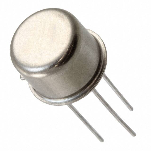
TO-5 Package
Also available in:
TO-39 (TO-205AD)
package
(leaded)
2N3439 – 2N3440
APPLICATIONS / BENEFITS
•
•
General purpose transistors for medium power applications requiring high frequency switching and
low package profile.
Military and other high-reliability applications.
U4 package
(surface mount)
2N3439U4 – 2N3440U4
UA package
(surface mount)
2N3439UA - 2N3440UA
MAXIMUM RATINGS (T C = +25°C unless otherwise noted)
Parameters / Test Conditions
Symbol
2N3439L
2N3440L
Unit
Collector-Emitter Voltage
V CEO
350
250
V
Collector-Base Voltage
V CBO
450
300
V
Emitter-Base Voltage
V EBO
7.0
V
IC
1.0
A
PD
0.8
5.0
W
TJ , Tstg
-65 to +200
°C
Collector Current
Total Power Dissipation
(1)
@ TA = +25 °C
(2)
@ TC = +25 °C
Operating & Storage Junction Temperature Range
Notes: 1. Derate linearly @ 4.57 mW/°C for TA > +25 °C.
2. Derate linearly @ 28.5 mW/°C for TC > +25 °C
MSC – Lawrence
6 Lake Street,
Lawrence, MA 01841
Tel: 1-800-446-1158 or
(978) 620-2600
Fax: (978) 689-0803
MSC – Ireland
Gort Road Business Park,
Ennis, Co. Clare, Ireland
Tel: +353 (0) 65 6840044
Fax: +353 (0) 65 6822298
Website:
www.microsemi.com
LDS-0022-1, Rev. 1 (111683)
©2011 Microsemi Corporation
Page 1 of 6
�2N3439L thru 2N3440L
MECHANICAL and PACKAGING
•
•
•
•
•
•
CASE: Hermetically sealed, kovar base, nickel cap.
TERMINALS: Tin/lead plate or RoHS compliant matte/tin (commercial grade only) over nickel.
MARKING: Part number, date code, manufacturer’s ID.
POLARITY: NPN (see package outline).
WEIGHT: Approximately 1.14 grams.
See Package Dimensions on last page.
PART NOMENCLATURE
JAN
2N3439
L
(e3)
Reliability Level
JAN = JAN Level
JANTX = JANTX Level
JANTXV = JANTXV Level
JANS = JANS Level
Blank = Commercial
RoHS Compliance
e3 = RoHS compliant (available
on commercial grade only)
Blank = non-RoHS compliant
Longer Lead Length
JEDEC type number
(see Electrical Characteristics
table)
Symbol
C obo
I CEO
I CEX
I EBO
h FE
V CEO
V CBO
V EBO
SYMBOLS & DEFINITIONS
Definition
Common-base open-circuit output capacitance.
Collector cutoff current, base open.
Collector cutoff current, circuit between base and emitter.
Emitter cutoff current, collector open.
Common-emitter static forward current transfer ratio.
Collector-emitter voltage, base open.
Collector-emitter voltage, emitter open.
Emitter-base voltage, collector open.
LDS-0022-1, Rev. 1 (111683)
©2011 Microsemi Corporation
Page 2 of 6
�2N3439L thru 2N3440L
ELECTRICAL CHARACTERISTICS (T A = +25°C, unless otherwise noted)
OFF CHARACTERISTICS
Parameters / Test Conditions
Collector-Emitter Breakdown Voltage
I C = 10 mA
R BB1 = 470 Ω; V BB1 = 6 V
L = 25 mH (min); f = 30 – 60 Hz
Collector-Emitter Cutoff Current
V CE = 300 V
V CE = 200 V
Emitter-Base Cutoff Current
V EB = 7.0 V
Collector-Emitter Cutoff Current
V CE = 450 V, V BE = -1.5 V
V CE = 300 V, V BE = -1.5 V
Collector-Base Cutoff Current
V CB = 360 V
V CB = 250 V
V CB = 450 V
V CB = 300 V
Symbol
Min.
2N3439L
2N3440L
V (BR)CEO
350
250
2N3439L
2N3440L
I CEO
2.0
2.0
µA
I EBO
10
µA
I CEX
5.0
5.0
µA
2N3439L
2N3440L
2N3439L
2N3440L
2N3439L
2N3440L
Max.
V
2.0
2.0
5.0
5.0
I CBO
Unit
µA
ON CHARACTERISTICS (1)
Parameters / Test Conditions
Forward-Current Transfer Ratio
I C = 20 mA, V CE = 10 V
I C = 2.0 mA, V CE = 10 V
I C = 0.2 mA, V CE = 10 V
Collector-Emitter Saturation Voltage
I C = 50 mA, I B = 4.0 mA
Base-Emitter Saturation Voltage
I C = 50 mA, I B = 4.0 mA
DYNAMIC CHARACTERISTICS
Parameters / Test Conditions
Symbol
h FE
Min.
Max.
40
30
10
160
Unit
V CE(sat)
0.5
V
V BE(sat)
1.3
V
Unit
Symbol
Min.
Max.
Magnitude of Common Emitter Small-Signal ShortCircuit Forward Current Transfer Ratio
I C = 10 mA, V CE = 10 V, f = 5.0 MHz
|h fe |
3.0
15
Forward Current Transfer Ratio
I C = 5.0 mA, V CE = 10 V, f = 1.0 kHz
h fe
25
Output Capacitance
V CB = 10 V, I E = 0, 100 kHz ≤ f ≤ 1.0 MHz
C obo
10
pF
Input Capacitance
V CB = 5.0 V, I E = 0, 100 kHz ≤ f ≤ 1.0 MHz
C ibo
75
pF
NOTES: (1) Pulse Test: Pulse Width = 300 µs, duty cycle ≤ 2.0%
LDS-0022-1, Rev. 1 (111683)
©2011 Microsemi Corporation
Page 3 of 6
�2N3439L thru 2N3440L
ELECTRICAL CHARACTERISTICS (T A = +25°C, unless otherwise noted) continued
SWITCHING CHARACTERISTICS
Parameters / Test Conditions
Symbol
Min.
Max.
Unit
Turn-On Time
V CC = 200 V; I C = 20 mA, I B1 = 2.0 mA
t on
1.0
µs
Turn-Off Time
V CC = 200 V; I C = 20 mA, I B1 = -I B2 = 2.0 mA
t off
10
µs
IC – Collector Current (mA)
SAFE OPERATING AREA (See graph below and also reference test method 3053 of
MIL-STD-750.)
DC Tests
T C = +25 °C, 1 Cycle, t = 1.0 s
Test 1
V CE = 5.0 V, I C = 1.0 A
Both Types
Test 2
V CE = 350 V, I C = 14 mA
2N3439L
Test 3
V CE = 250 V, I C = 20 mA
2N3440L
V CE – Collector to Emitter Voltage (V)
Maximum Safe Operating graph (continuous dc)
LDS-0022-1, Rev. 1 (111683)
©2011 Microsemi Corporation
Page 4 of 6
�2N3439L thru 2N3440L
DC Operation Maximum Rating (W)
GRAPHS
o
TC ( C) (Case)
FIGURE 1
Temperature-Power Derating Curve
o
THETA (oC/W)
NOTES: Thermal Resistance Junction to Case = 30.0 C/W
o
Max Finish-Alloy Temp = 175.0 C
.110-5
.110-4
.110-3
.110-2 .110-1
TIME (s)
0.1
1
10
100
FIGURE 2
Maximum Thermal Impedance
NOTE: T C = +25 °C, P T = 5.0 W, thermal resistance R θJC = 30 °C/W, steel.
LDS-0022-1, Rev. 1 (111683)
©2011 Microsemi Corporation
Page 5 of 6
�2N3439L thru 2N3440L
PACKAGE DIMENSIONS
Symbol
CD
CH
HD
LC
LD
LL
LU
Dimensions
Millimeters
Min
Max
Min
Max
.305
.335
7.75
8.51
.240
.260
6.10
6.60
.335
.370
8.51
9.40
.200 TP
5.08 TP
.016
.019
0.41
0.48
See note 14
.016
.019
0.41
0.48
Inches
L1
.050
L2
.250
P
Q
TL
TW
r
α
.100
.029
.028
45° TP
1.27
6.35
6
7
8,9
8,9
8,9
8,9
2.54
.030
.045
.034
.010
Note
0.76
1.14
0.86
0.25
0.74
0.71
45° TP
7
5
3,4
3
10
7
NOTES:
1.
2.
3.
4.
5.
6.
7.
8.
9.
10.
11.
12.
13.
14.
Dimensions are in inches.
Millimeters are given for general information only.
Beyond r (radius) maximum, TW shall be held for a minimum length of .011 (0.28 mm).
Dimension TL measured from maximum HD.
Body contour optional within zone defined by HD, CD, and Q.
CD shall not vary more than .010 inch (0.25 mm) in zone P. This zone is controlled for automatic handling.
Leads at gauge plane .054 +.001 -.000 inch (1.37 +0.03 -0.00 mm) below seating plane shall be within .007 inch (0.18 mm)
radius of true position (TP) at maximum material condition (MMC) relative to tab at MMC. The device may be measured by
direct methods or by gauging procedure.
Dimension LU applies between L1 and L2. Dimension LD applies between L2 and LL minimum. Diameter is uncontrolled in
and beyond LL minimum.
All three leads.
The collector shall be internally connected to the case.
Dimension r (radius) applies to both inside corners of tab.
In accordance with ASME Y14.5M, diameters are equivalent to Φx symbology.
Lead 1 = emitter, lead 2 = base, lead 3 = collector.
For transistor types 2N3439L and 2N3440L (TO-5), dimension LL = 1.5 inches (38.10 mm) min. and 1.75 inches (44.45 mm)
max.
LDS-0022-1, Rev. 1 (111683)
©2011 Microsemi Corporation
Page 6 of 6
�