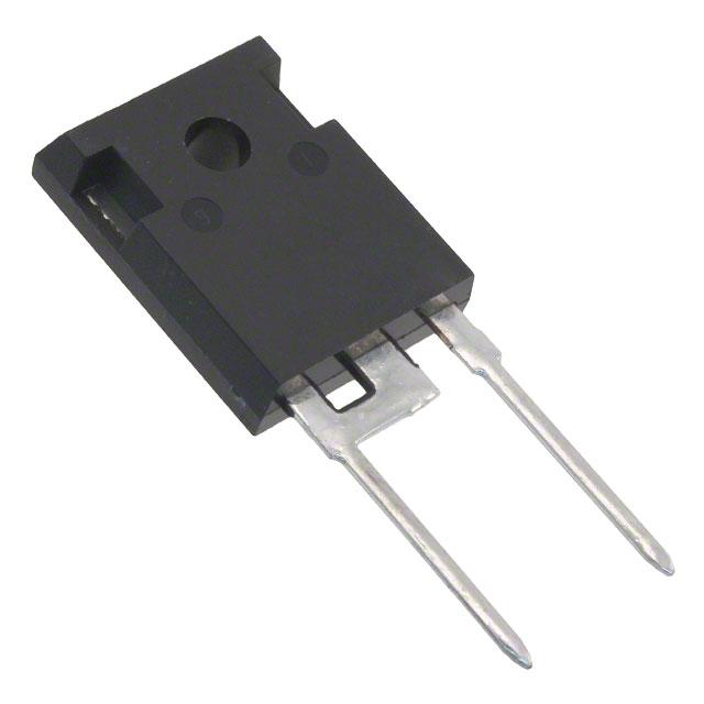
APT30D60BG Fast Soft Recovery Rectifier Diode
Product Overview
The APT30D60BG device is a 600 V, 30 A Fast Soft Recovery Rectifier Si Diode in a TO-247 package.
Features
The following are key features of the APT30D60BG device:
• Fast recovery times
• Soft recovery characteristics
• Low forward voltage
• Low leakage current
• RoHS compliant
Benefits
The following are benefits of the APT30D60BG device:
• Low switching losses
• Low noise (EMI) switching
• Cooler operation
• Higher reliability systems
• Increased system power density
Applications
The APT30D60BG device is designed for the following applications:
• Power factor correction (PFC)
• Anti-parallel diode
◦ Switch-mode power supply
◦ Inverters
• Freewheeling diode
◦ Motor controllers
◦ Inverters/converters
• Snubber diode
053-6002 APT30D60BG Data Sheet Revision I
1
�Device Specifications
Device Specifications
This section shows the specifications of the APT30D60BG device.
Absolute Maximum Ratings
The following table shows the absolute maximum ratings of the APT30D60BG device.
TC = 25 °C, unless otherwise specified.
Table 1 • Absolute Maximum Ratings
Symbol
Parameter
Rating
Unit
VR
Maximum DC reverse voltage
600
V
VRRM
Maximum peak repetitive reverse voltage
VRWM
Maximum working peak reverse voltage
IF(AV)
Maximum average forward current (TC = 140 °C, duty cycle = 0.5)
30
A
IFSM
Non-repetitive forward surge current (TJ = 45 °C, 8.3 ms)
320
The following table shows the thermal and mechanical characteristics of the APT30D60BG device.
Table 2 • Thermal and Mechanical Characteristics
Symbol
Characteristic
RθJC
Min
Typ
Max
Unit
Junction-to-case thermal resistance
0.67
°C/W
RθJA
Junction-to-ambient thermal resistance
40
TJ, TSTG
Operating and storage temperature range
TL
Lead temperature for 10 seconds
Wt
Package weight
–55
Mounting torque, 6-32 or M3 screw
053-6002 APT30D60BG Data Sheet Revision I
175
°C
300
0.22
oz
6.2
g
10
lbf•m
1.1
N•m
2
�Device Specifications
Electrical Performance
The following table shows the static characteristics of the APT30D60BG device. TJ = 25 °C, unless otherwise
specified.
Table 3 • Static Characteristics
Symbol
Characteristic
Test Conditions
VF
Forward voltage
IRM
CJ
Maximum reverse leakage current
Junction capacitance
Min
Typ
Max
Unit
IF = 30 A
1.6
1.8
V
IF = 60 A
1.9
IF = 30 A, TJ = 125 °C
1.4
VR = VR rated
250
µA
VR = VR rated, TJ = 125 °C
500
VR = 200 V
44
pF
The following table shows the dynamic characteristics of the APT30D60BG device.
Table 4 • Dynamic Characteristics
Symbol
Characteristic
Test Conditions
trr
Reverse recovery time
IF = 1 A, diF/dt = –100 A/µs
Min
Typ
Max
Unit
23
ns
85
ns
VR = 30 V
trr
Reverse recovery time
IF = 30 A, diF/dt = –200 A/µs
Qrr
Reverse recovery charge
130
nC
IRRM
Maximum reverse recovery current
4
A
trr
Reverse recovery time
160
ns
VR = 400 V
IF = 30 A, diF/dt = –200 A/µs
VR = 400 V, TJ = 125 °C
Qrr
Reverse recovery charge
700
nC
IRRM
Maximum reverse recovery current
8
A
trr
Reverse recovery time
70
ns
IF = 30 A, diF/dt = –1000 A/µs
VR = 400 V, TJ = 125 °C
Qrr
Reverse recovery charge
1300
nC
IRRM
Maximum reverse recovery current
30
A
053-6002 APT30D60BG Data Sheet Revision I
3
�Device Specifications
Typical Performance Curves
This section shows the typical performance curves of the APT30D60BG device.
Figure 1 • Maximum Transient Thermal Impedance
Figure 2 • Forward Current vs. Forward Voltage
Figure 3 • Reverse Recovery Time vs. Current Rate
of Change
053-6002 APT30D60BG Data Sheet Revision I
4
�Device Specifications
Figure 4 • Reverse Recovery Charge vs. Current
Rate of Change
Figure 5 • Reverse Recovery Current vs. Current
Rate of Change
Figure 6 • Dynamic Parameters vs. Junction
Temperature
Figure 7 • Maximum Average Forward Current vs.
Case Temperature
Figure 8 • Junction Capacitance vs. Reverse Voltage
053-6002 APT30D60BG Data Sheet Revision I
5
�Device Specifications
Reverse Recovery Overview
The following figure illustrates the diode test circuit of the APT30D60BG device.
Figure 9 • Diode Test Circuit
The following figure illustrates the diode reverse recovery waveform and definitions of the APT30D60BG
device.
Figure 10 • Diode Reverse Recovery Waveform and Definitions
1. IF—Forward conduction current.
2. diF/dt—Rate of diode current change through zero crossing.
3. IRRM—Maximum reverse recovery current.
4. trr—Reverse recovery time, measured from zero crossing where diode current goes from positive to
negative, to the point at which the straight line through IRRM and 0.25 • IRRM passes through zero.
5. Qrr—Area under the curve defined by IRRM and trr.
053-6002 APT30D60BG Data Sheet Revision I
6
�Package Specification
Package Specification
This section shows the package specification of the APT30D60BG device.
Package Outline Drawing
The following figure illustrates the TO-247 (B) package outline of the APT30D60BG device.
Figure 11 • Package Outline Drawing
053-6002 APT30D60BG Data Sheet Revision I
7
�Package Specification
The following table shows the TO-247 dimensions and should be used in conjunction with the package
outline drawing.
Table 5 • TO-247 Dimensions
SYMBOL
MIN
MAX
MIN
MAX
[mm]
[mm]
[INCH]
[INCH]
A
4.69
5.31
0.185
0.209
B
1.49
2.49
0.059
0.098
C
2.21
2.59
0.087
0.102
D
0.40
0.79
0.016
0.031
E
5.38
6.20
0.212
0.244
F
3.50
3.81
0.138
0.150
G
6.15 BSC
H
20.80
21.46
0.819
0.845
I
19.81
20.32
0.780
0.800
J
4.00
4.50
0.157
0.177
K
1.01
1.40
0.040
0.055
L
2.87
3.12
0.113
0.123
M
1.65
2.13
0.065
0.084
N
15.49
16.26
0.610
0.640
O
13.50
14.50
0.531
0.571
P
16.50
17.50
0.650
0.689
Q
5.45 BSC
R
2.00
2.75
0.079
0.108
S
7.10
7.50
0.280
0.295
TERMINAL 1
CATHODE
TERMINAL 2
ANODE
TERMINAL 3
CATHODE
0.242 BSC
0.215 BSC
053-6002 APT30D60BG Data Sheet Revision I
8
�Legal
Microsemi
2355 W. Chandler Blvd.
Chandler, AZ 85224 USA
Within the USA: +1 (480) 792-7200
Fax: +1 (480) 792-7277
www.microsemi.com © 2020 Microsemi and
its corporate affiliates. All rights reserved.
Microsemi and the Microsemi logo are
trademarks of Microsemi Corporation and its
corporate affiliates. All other trademarks and
service marks are the property of their
respective owners.
Microsemi's product warranty is set forth in Microsemi's Sales Order Terms and Conditions. Information
contained in this publication is provided for the sole purpose of designing with and using Microsemi
products. Information regarding device applications and the like is provided only for your convenience
and may be superseded by updates. Buyer shall not rely on any data and performance specifications or
parameters provided by Microsemi. It is your responsibility to ensure that your application meets with
your specifications. THIS INFORMATION IS PROVIDED "AS IS." MICROSEMI MAKES NO REPRESENTATIONS
OR WARRANTIES OF ANY KIND WHETHER EXPRESS OR IMPLIED, WRITTEN OR ORAL, STATUTORY OR
OTHERWISE, RELATED TO THE INFORMATION, INCLUDING BUT NOT LIMITED TO ITS CONDITION, QUALITY,
PERFORMANCE, NON-INFRINGEMENT, MERCHANTABILITY OR FITNESS FOR A PARTICULAR PURPOSE.
IN NO EVENT WILL MICROSEMI BE LIABLE FOR ANY INDIRECT, SPECIAL, PUNITIVE, INCIDENTAL OR
CONSEQUENTIAL LOSS, DAMAGE, COST OR EXPENSE WHATSOEVER RELATED TO THIS INFORMATION
OR ITS USE, HOWEVER CAUSED, EVEN IF MICROSEMI HAS BEEN ADVISED OF THE POSSIBILITY OR THE
DAMAGES ARE FORESEEABLE. TO THE FULLEST EXTENT ALLOWED BY LAW, MICROSEMI’S TOTAL LIABILITY
ON ALL CLAIMS IN RELATED TO THIS INFORMATION OR ITS USE WILL NOT EXCEED THE AMOUNT OF
FEES, IF ANY, YOU PAID DIRECTLY TO MICROSEMI FOR THIS INFORMATION. Use of Microsemi devices
in life support, mission-critical equipment or applications, and/or safety applications is entirely at the
buyer’s risk, and the buyer agrees to defend and indemnify Microsemi from any and all damages, claims,
suits, or expenses resulting from such use. No licenses are conveyed, implicitly or otherwise, under any
Microsemi intellectual property rights unless otherwise stated.
Microsemi Corporation, a subsidiary of Microchip Technology Inc. (Nasdaq: MCHP),
and its corporate affiliates are leading providers of smart, connected and secure
embedded control solutions. Their easy-to-use development tools and
comprehensive product portfolio enable customers to create optimal designs which
reduce risk while lowering total system cost and time to market. These solutions
serve more than 120,000 customers across the industrial, automotive, consumer,
aerospace and defense, communications and computing markets. Headquartered
in Chandler, Arizona, the company offers outstanding technical support along with
dependable delivery and quality. Learn more at www.microsemi.com.
053-6002 | April 2020 | Released
053-6002 APT30D60BG Data Sheet Revision I
9
�