ARF461A(G)
ARF461B(G)
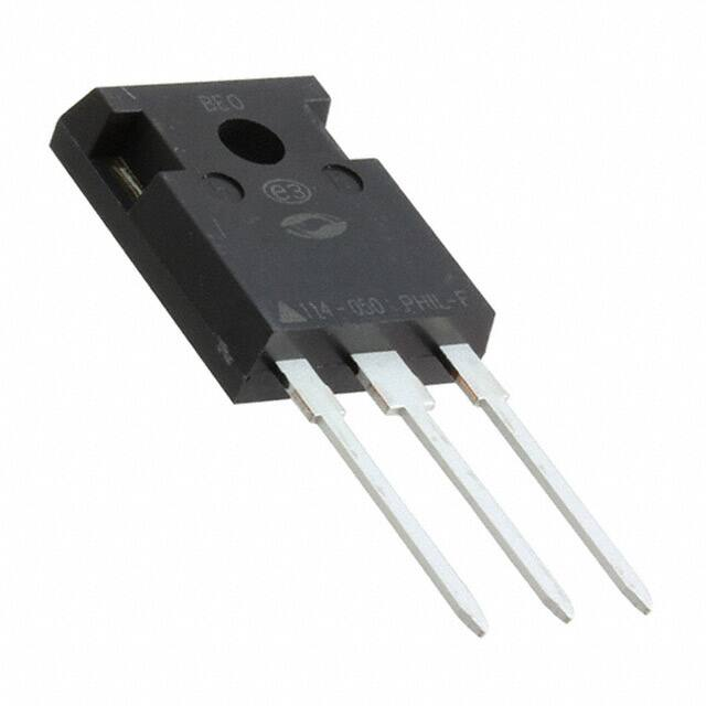
TO
-24
7
Common
Source
RF POWER MOSFETs
N - CHANNEL ENHANCEMENT MODE
250V
150W
65MHz
The ARF461A and ARF461B comprise a symmetric pair of common drain RF power transistors designed for pushpull scientific, commercial, medical and industrial RF power amplifier applications up to 65 MHz. They have been
optimized for both linear and high efficiency classes of operation.
• Specified 250 Volt, 40.68 MHz Characteristics:
•
Output Power = 150 Watts.
•
Gain = 13dB (Class AB)
•
Efficiency = 75% (Class C)
• Low Cost Common Source RF Package.
• Low Vth thermal coefficient.
• Low Thermal Resistance.
• Optimized SOA for Superior Ruggedness.
• RoHS Compliant
All Ratings: TC = 25°C unless otherwise specified.
MAXIMUM RATINGS
Symbol
Parameter
ARF461AG/BG
VDSS
Drain-Source Voltage
1000
VDGO
Drain-Gate Voltage
1000
ID
Unit
V
Continuous Drain Current @ TC = 25°C
6.5
A
VGS
Gate-Source Voltage
±30
V
PD
Total Power Dissipation @ TC = 25°C
250
W
0.50
°C/W
RθJC
TJ, TSTG
TL
Junction to Case
Operating and Storage Junction Temperature Range
-55 to 150
Lead Temperature: 0.063” from Case for 10 Sec.
°C
300
STATIC ELECTRICAL CHARACTERISTICS
Parameter
Min
BVDSS
Drain-Source Breakdown Voltage (VGS = 0V, ID = 250 μA)
1000
VDS(ON)
On State Drain Voltage 1 (ID(ON) = 3.25A, VGS = 10V)
6.5
Zero Gate Voltage Drain Current (VDS = VDSS, VGS = 0V)
25
Zero Gate Voltage Drain Current (VDS = 0.8VDSS, VGS = 0, TC = 125°C)
250
IGSS
Gate-Source Leakage Current (VDS = ±30V, VDS = 0V)
gfs
Forward Transconductance (VDS = 25V, ID = 3.25A)
3
Gate Threshold Voltage (VDS = VGS, ID = 50mA)
3
VGS(TH)
Max
±100
4
CAUTION: These Devices are Sensitive to Electrostatic Discharge. Proper Handling Procedures Should Be Followed.
Microsemi Website - http://www.microsemi.com
Unit
V
μA
nA
mhos
5
Volts
6-2008
IDSS
Typ
050-5987 Rev D
Symbol
�Dynamic Characteristics
Symbol
ARF461A/B
Parameter
Test Conditions
Min
Typ
CISS
Input Capacitance
VGS = 0V
1700
Coss
Output Capacitance
VDS = 50V
175
Crss
Reverse Transfer Capacitance
f = 1MHz
50
td(on)
Turn-On Delay Time
tr
td(off)
Turn-off Delay Time
tf
Fall Time
Unit
pF
8
VGS = 15V
Rise Time
Max
VDD = 0.5VDSS
5
ID = ID (Cont.) @ 25°C
21
RG = 1.6Ω
10.1
ns
Functional Characteristics
Symbol
Characteristic
GPS
1
Test Conditions
Min
Typ
f = 40.68MHz
13
15
dB
VGS = 0V VDD = 250V
70
75
%
Common Source Amplifier Power Gain
η
Drain Efficiency
Ψ
Electrical Ruggedness VSWR 10:1
POUT = 150W
Max
Unit
No Degradation in Output Power
Pulse Test: Pulse width < 380 μS, Duty Cycle < 2%
APT Reserves the right to change, without notice, the specifications and information contained herein.
5000
30
Class C
VDD = 150V
25
1000
CAPACITANCE (pf)
20
GAIN (dB)
Ciss
Pout = 150W
15
10
500
Coss
100
Crss
50
5
ID, DRAIN CURRENT (AMPERES)
050-5987 Rev D
6-2008
8
6
.1
.5 1
5 10
50
200
VDS, DRAIN-TO-SOURCE VOLTAGE (VOLTS)
Figure 2, Typical Capacitance vs. Drain-to-Source Voltage
60
75
90
105
120
FREQUENCY (MHz)
Figure 1, Typical Gain vs Frequency
26
TJ = -55°C
VDS> ID (ON) x RDS (ON)MAX.
250μSEC. PULSE TEST
@
很抱歉,暂时无法提供与“ARF461AG”相匹配的价格&库存,您可以联系我们找货
免费人工找货- 国内价格 香港价格
- 1+532.562201+68.65754