ARF465A
ARF465B
D
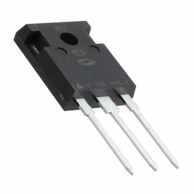
G
S
TO-247
Common
Source
RF POWER MOSFETs
N - CHANNEL ENHANCEMENT MODE
300V 150W
60MHz
The ARF465A and 465B comprise a symmetric pair of common source RF power transistors designed for push-pull
scientific, commercial, medical and industrial RF power amplifier applications up to 60 MHz.
• Specified 300 Volt, 40.68 MHz Characteristics:
•
Output Power = 150 Watts.
•
Gain = 13dB (Class C)
•
Efficiency = 75%
• Low Cost Common Source RF Package.
• Low Vth thermal coefficient.
• Low Thermal Resistance.
• Optimized SOA for Superior Ruggedness.
MAXIMUM RATINGS
Symbol
All Ratings: TC = 25°C unless otherwise specified.
Parameter
ARF465A/B
VDSS
Drain-Source Voltage
1200
VDGO
Drain-Gate Voltage
1200
ID
UNIT
Volts
Continuous Drain Current @ TC = 25°C
6
Amps
VGS
Gate-Source Voltage
±30
Volts
PD
Total Power Dissipation @ TC = 25°C
250
Watts
Junction to Case
0.50
°C/W
RθJC
TJ,TSTG
TL
-55 to 150
Operating and Storage Junction Temperature Range
°C
300
Lead Temperature: 0.063" from Case for 10 Sec.
STATIC ELECTRICAL CHARACTERISTICS
MIN
Drain-Source Breakdown Voltage (VGS = 0V, ID = 250 µA)
1200
VDS(ON) On State Drain Voltage
IDSS
IGSS
1
TYP
MAX
Volts
(I D(ON) = 3A, VGS = 10V)
7
Zero Gate Voltage Drain Current (VDS = VDSS, VGS = 0V)
25
µA
Zero Gate Voltage Drain Current (VDS = 0.8 VDSS, VGS = 0V, TC = 125°C)
250
Gate-Source Leakage Current (VGS = ±30V, VDS = 0V)
±100
gfs
Forward Transconductance (VDS = 25V, ID = 3A)
3
VGS(TH)
Gate Threshold Voltage (VDS = VGS, ID = 50mA)
3
4
CAUTION: These Devices are Sensitive to Electrostatic Discharge. Proper Handling Procedures Should Be Followed.
APT Website - http://www.advancedpower.com
Downloaded from Elcodis.com electronic components distributor
UNIT
nA
mhos
5
Volts
7-2003
BVDSS
Characteristic / Test Conditions
050-4921 Rev A
Symbol
�DYNAMIC CHARACTERISTICS
Symbol
ARF465A/B
Test Conditions
Characteristic
Ciss
Input Capacitance
Coss
Output Capacitance
Crss
Reverse Transfer Capacitance
td(on)
Turn-on Delay Time
tr
td(off)
tf
MIN
TYP
MAX
1200
1500
VDS = 200V
80
100
f = 1 MHz
30
50
VGS = 15V
7
15
VDD = 0.5 VDSS
5
10
ID = ID[Cont.] @ 25°C
21
34
RG = 1.6Ω
12
25
MAX
VGS = 0V
Rise Time
Turn-off Delay Time
Fall Time
UNIT
pF
ns
FUNCTIONAL CHARACTERISTICS
Symbol
GPS
η
ψ
Characteristic
Common Source Amplifier Power Gain
Test Conditions
MIN
TYP
f = 40.68 MHz
13
15
dB
70
75
%
VGS = 0V
Drain Efficiency
Electrical Ruggedness VSWR 6:1
VDD = 300V
Pout = 150W
UNIT
No Degradation in Output Power
1 Pulse Test: Pulse width < 380 µS, Duty Cycle < 2%
APT Reserves the right to change, without notice, the specifications and information contained herein.
10,000
25
Class C
VDD = 300V
CAPACITANCE (pf)
GAIN (dB)
5000
Pout = 150W
20
15
10
10
0.1
1
10
100 300
VDS, DRAIN-TO-SOURCE VOLTAGE (VOLTS)
Figure 2, Typical Capacitance vs. Drain-to-Source Voltage
40 50 60 70
80 90 100
FREQUENCY (MHz)
Figure 1, Typical Gain vs Frequency
30
24
VDS> ID (ON) x RDS (ON)MAX.
250µSEC. PULSE TEST
@
很抱歉,暂时无法提供与“ARF465BG”相匹配的价格&库存,您可以联系我们找货
免费人工找货