物料型号:ARF466A(G) 和 ARF466B(G)
器件简介:ARF466A和ARF466B是一对对称的共源RF功率晶体管,设计用于45MHz以下的推挽科学、商业、医疗和工业RF功率放大器应用。
它们针对线性和高效率类别的操作进行了优化。
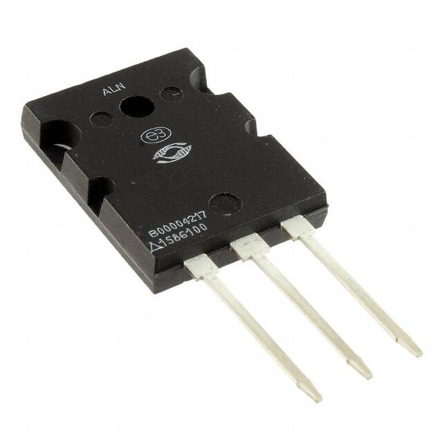
引脚分配:ARF466A和ARF466B的引脚布局是彼此的镜像,以便于作为推挽对使用。
引脚包括漏极、栅极和源极。
参数特性:在150V、40.68MHz的条件下,输出功率为300瓦,增益为16dB(AB类),效率为75%(C类)。
具有低成本的共源RF封装、低Vth热系数、低热阻和优化的SOA以提高鲁棒性。
功能详解:器件对静电放电敏感,需要遵循适当的处理程序。
提供了详细的静态电气特性、动态特性和功能特性,包括转移特性、最大安全工作区和热阻抗等。
应用信息:适用于推挽配置的RF功率放大器,特别是在需要高效率和线性操作的场合。
封装信息:TO-264封装,详细尺寸和引脚布局在文档中有描述。
ARF466A和ARF466B的封装尺寸相同,便于作为推挽对使用。