VRF2933
50V, 300W, 150MHz
RF POWER VERTICAL MOSFET
The VRF2933 is a gold-metallized silicon n-channel RF power transistor designed for broadband commercial and military applications requiring high power
and gain without compromising reliability, ruggedness, or inter-modulation
distortion.
FEATURES
• Improved Ruggedness V(BR)DSS = 170V
• 3:1 Load VSWR Capability at Specified Operating Conditions
• 300W with 20dB Min. Gain @ 30MHz, 50V
• Nitride Passivated
• Excellent Stability & Low IMD
• Refractory Gold Metallization
• Common Source Configuration
• Improved Replacement for SD2933
• RoHS Compliant
• Thermally Enhanced Package
Maximum Ratings
Symbol
VDSS
ID
All Ratings: TC =25°C unless otherwise specified
Parameter
Drain-Source Voltage
VRF2933
Unit
170
V
Continuous Drain Current @ TC = 25°C
40
A
VGS
Gate-Source Voltage
±40
V
PD
Total Device dissipation @ TC = 25°C
648
W
TSTG
TJ
Storage Temperature Range
-65 to 150
Operating Junction Temperature Max
°C
200
Static Electrical Characteristics
Symbol
Parameter
Min
Typ
V(BR)DSS
Drain-Source Breakdown Voltage (VGS = 0V, ID = 100mA)
170
180
VDS(ON)
On State Drain Voltage (ID(ON) = 20A, VGS = 10V)
2.0
Max
5.0
Unit
V
IDSS
Zero Gate Voltage Drain Current (VDS = 100V, VGS = 0V)
2.0
mA
IGSS
Gate-Source Leakage Current (VDS = ±20V, VDS = 0V)
2.0
μA
gfs
Forward Transconductance (VDS = 10V, ID = 20A)
8
VGS(TH)
Gate Threshold Voltage (VDS = 10V, ID = 100mA)
2.9
3.6
4.4
V
Min
Typ
Max
Unit
0.27
°C/W
mhos
Symbol
RθJC
Characteristic
Junction to Case Thermal Resistance
CAUTION: These Devices are Sensitive to Electrostatic Discharge. Proper Handling Procedures Should Be Followed.
Microsemi Website - http://www.microsemi.com
Downloaded from Elcodis.com electronic components distributor
050-4941 Rev E 7-2008
Thermal Characteristics
�Dynamic Characteristics
Symbol
VRF2933
Parameter
Test Conditions
Min
Typ
CISS
Input Capacitance
VGS = 0V
740
Coss
Output Capacitance
VDS = 50V
400
Crss
Reverse Transfer Capacitance
f = 1MHz
32
Max
Unit
pF
Functional Characteristics
Symbol
Parameter
GPS
f1 = 30MHz, VDD = 50V, IDQ = 250mA, Pout = 300W
ηD
f1 = 175MHz, VDD = 50V, IDQ = 250mA, Pout = 300W
ψ
f1 = 30MHz, VDD = 50V, IDQ = 250mA, Pout = 300W
Min
Typ
18
22
Max
dB
50
%
No Degradation in Output Power
3:1 VSWR - All Phase Angles
1. To MIL-STD-1311 Version A, test method 2204B, Two Tone, Reference Each Tone
Microsemi reserves the right to change, without notice, the specifications and information contained herein.
Typical Performance Curves
30
55
50
45
25
6.5V
ID, DRAIN CURRENT (A)
6V
35
30
5.5V
25
20
5V
15
4.5V
10
4V
3.5V
5
0
0
V
5
10
15
15
10
5
TJ= 125°C
0
, DRAIN-TO-SOURCE VOLTAGE (V)
DS(ON)
FIGURE 1, Output Characteristics
2
4
6
8
VDS, DRAIN-TO-SOURCE VOLTAGE (V)
FIGURE 2, Transfer Characteristics
100
ID, DRAIN CURRENT (V)
Ciss
1.0E−9
C, CAPACITANCE (F)
TJ= 25°C
20
0
20
1.0E−8
Coss
1.0E−10
Crss
1.0E−11
TJ= -55°C
0
10
20
30
40
50
60
VDS, GATE-TO-SOURCE VOLTAGE (V)
FIGURE 3, Capacitance vs Drain-to-Source Voltage
Downloaded from Elcodis.com electronic components distributor
BVdss Line
ID, DRAIN CURRENT (A)
40
050-4941 Rev E 7-2008
250μs PULSE
TEST
很抱歉,暂时无法提供与“VRF2933”相匹配的价格&库存,您可以联系我们找货
免费人工找货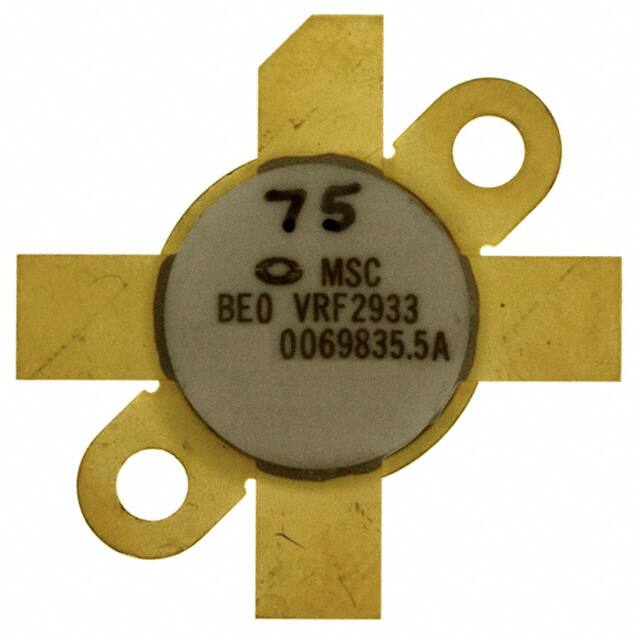


 工商网监
湘ICP备2023018690号
工商网监
湘ICP备2023018690号
