FEATURES
FUNCTIONAL BLOCK DIAGRAM
Frequency range: 5.9 GHz to 8.5 GHz
Typical gain of 25 dB
Low noise input
Noise figure: 4.0 dBm typical input third-order intercept (IIP3)
>−10.6 dBm typical input 1 dB compression point (P1dB)
Matched 50 Ω single-ended input
Matched 100 Ω differential outputs
8-lead, 2.00 mm × 2.00 mm LFCSP microwave packaging
VCC1
50Ω
SINGLE-ENDED
ADL5721
VCC2
GND
OUTN
INPT
OUTP
RBIAS
BAND
100Ω
DIFFERENTIAL
14258-001
Data Sheet
5.9 GHz to 8.5 GHz, Low Noise Amplifier
ADL5721
Figure 1.
APPLICATIONS
Point to point microwave radios
Instrumentation
Satellite communications (SATCOM)
Phased arrays
GENERAL DESCRIPTION
The ADL5721 is a narrow-band, high performance, low noise
amplifier targeting microwave radio link receiver designs. The
monolithic silicon germanium (SiGe) design is optimized for
microwave radio link bands ranging from 5.9 GHz to 8.5 GHz.
The unique design offers a single-ended 50 Ω input impedance
and provides a 100 Ω balanced differential output that is ideal
for driving Analog Devices, Inc., differential downconverters
and radio frequency (RF) sampling analog-to-digital converters
(ADCs). This low noise amplifier (LNA) provides noise figure
Rev. 0
performance that, in the past, required more expensive threefive (III-V) compounds process technology to achieve. This
LNA uses a band switch feature to allow the input P1dB and
noise figure to trade off for optimum system performance.
The ADL5721 and ADL5723 to ADL5726 family of narrowband LNAs are each packaged in a tiny, thermally enhanced,
2.00 mm × 2.00 mm LFCSP package. The ADL5721 and
ADL5723 to ADL5726 family operates over the temperature
range of −40°C to +85°C.
Document Feedback
Information furnished by Analog Devices is believed to be accurate and reliable. However, no
responsibility is assumed by Analog Devices for its use, nor for any infringements of patents or other
rights of third parties that may result from its use. Specifications subject to change without notice. No
license is granted by implication or otherwise under any patent or patent rights of Analog Devices.
Trademarks and registered trademarks are the property of their respective owners.
One Technology Way, P.O. Box 9106, Norwood, MA 02062-9106, U.S.A.
Tel: 781.329.4700
©2016 Analog Devices, Inc. All rights reserved.
Technical Support
www.analog.com
�ADL5721
Data Sheet
TABLE OF CONTENTS
Features .............................................................................................. 1
Low Band (BAND = 0 V) .............................................................6
Applications ....................................................................................... 1
High Band (BAND = 1.8 V) ........................................................8
Functional Block Diagram .............................................................. 1
Theory of Operation ...................................................................... 10
General Description ......................................................................... 1
Applications Information .............................................................. 11
Revision History ............................................................................... 2
Layout .......................................................................................... 11
Specifications..................................................................................... 3
Differential vs. Single-Ended Output ...................................... 11
AC Specifications.......................................................................... 3
Evaluation Board ............................................................................ 13
DC Specifications ......................................................................... 3
Initial Setup ................................................................................. 13
Absolute Maximum Ratings ............................................................ 4
Results .......................................................................................... 13
Thermal Resistance ...................................................................... 4
Basic Connections for Operation ............................................. 14
ESD Caution .................................................................................. 4
Outline Dimensions ....................................................................... 15
Pin Configuration and Function Descriptions ............................. 5
Ordering Guide .......................................................................... 15
Typical Performance Characteristics ............................................. 6
REVISION HISTORY
4/16—Revision 0: Initial Version
Rev. 0 | Page 2 of 15
�Data Sheet
ADL5721
SPECIFICATIONS
AC SPECIFICATIONS
TA = 25°C, VCC1 = 1.8 V, VCC2 = 3.3 V, ZSOURCE = 50 Ω, ZLOAD = 100 Ω differential, unless otherwise noted.
Table 1.
Parameter
FREQUENCY RANGE
Low Band, BAND = 0 V
High Band, BAND = 1.8 V
FREQUENCY = 5.9 GHz
Gain (S21)
Noise Figure
Input Third-Order Intercept (IIP3)
Input 1 dB Compression Point (P1dB)
Input Return Loss (S11)
Output Return Loss (S22)
FREQUENCY = 7.2 GHz
Gain (S21)
Noise Figure
Input Third-Order Intercept (IIP3)
Input 1 dB Compression Point (P1dB)
Input Return Loss (S11)
Output Return Loss (S22)
FREQUENCY = 8.5 GHz
Gain (S21)
Noise Figure
Input Third-Order Intercept (IIP3)
Input 1 dB Compression Point (P1dB)
Input Return Loss (S11)
Output Return Loss (S22)
Test Conditions/Comments
Min
Typ
5.9
7.1
Max
Unit
7.2
8.5
GHz
GHz
Low band, BAND = 0 V
Δf = 1 MHz, input power (PIN) = −30 dBm per tone
25.0
1.7
4.3
−10.6
10
9
dB
dB
dBm
dBm
dB
dB
25.9
1.6
4.0
−9.3
10
10
dB
dB
dBm
dBm
dB
dB
24.6
1.5
5.7
−8.6
10
10
dB
dB
dBm
dBm
dB
dB
Low band, BAND = 0 V
Δf = 1 MHz, PIN = −30 dBm per tone
High band, BAND = 1.8 V
Δf = 1 MHz, PIN = −30 dBm per tone
DC SPECIFICATIONS
Table 2.
Parameter
POWER INTERFACE
VCC1 Voltage
VCC2 Voltage
Quiescent Current vs. Temperature
VCC1
VCC2
Test Conditions/Comments
TA = 25°C
−40°C ≤ TA ≤ +85°C
TA = 25°C
−40°C ≤ TA ≤ +85°C
Rev. 0 | Page 3 of 15
Min
Typ
Max
Unit
1.65
3.1
1.8
3.3
1.95
3.5
V
V
11.6
12.1
74.1
74.4
mA
mA
mA
mA
�ADL5721
Data Sheet
ABSOLUTE MAXIMUM RATINGS
THERMAL RESISTANCE
Table 3.
Parameter
Supply Voltages
VCC1
VCC2
Maximum Junction Temperature
Operating Temperature Range
Storage Temperature Range
Lead Temperature Range (Soldering 60 sec)
Rating
2.25 V
4.1 V
150°C
−40°C to +85°C
−55°C to +125°C
−65°C to +150°C
Stresses at or above those listed under Absolute Maximum
Ratings may cause permanent damage to the product. This is a
stress rating only; functional operation of the product at these
or any other conditions above those indicated in the operational
section of this specification is not implied. Operation beyond
the maximum operating conditions for extended periods may
affect product reliability.
θJA is thermal resistance, junction to ambient (°C/W), θJB is
thermal resistance, junction to board (°C/W), and θJC is thermal
resistance, junction to case (°C/W).
Table 4. Thermal Resistance
Package Type
8-Lead LFCSP
1
θJA1
39.90
θJB1
23.88
θJC1
3.71
Unit
°C/W
See JEDEC standard JESD51-2 for additional information on optimizing the
thermal impedance for a printed circuit board (PCB) with 3 × 4 vias.
ESD CAUTION
Rev. 0 | Page 4 of 15
�Data Sheet
ADL5721
PIN CONFIGURATION AND FUNCTION DESCRIPTIONS
VCC1 1
INPT 3
RBIAS 4
8 VCC2
ADL5721
TOP VIEW
(Not to Scale)
7 OUTN
6 OUTP
5 BAND
NOTES
1. THE EXPOSED PAD MUST BE
SOLDERED TO A LOW IMPEDANCE
GROUND PLANE.
2. THE DEVICE NUMBER ON THE FIGURE
DOES NOT INDICATE THE LABEL ON
THE PACKAGE. REFER TO THE PIN 1
INDICATOR FOR THE PIN LOCATIONS.
14258-002
GND 2
Figure 2. Pin Configuration
Table 5. Pin Function Descriptions
Pin No.
1
2
3
4
Mnemonic
VCC1
GND
INPT
RBIAS
5
BAND
6, 7
8
OUTP, OUTN
VCC2
EPAD (EP)
Description
1.8 V Power Supply. It is recommended to place the decoupling capacitors as close to this pin as possible.
Ground.
RF Input. This pin is a 50 Ω single-ended input.
Resistor Bias. For typical operation, connect a 442 Ω resistor from RBIAS to GND. It is recommended to
place the RBIAS resistor as close to the pin as possible.
Band Select Control. Select a logic low of 0 V for the lower frequency range from 5.9 GHz to 7.2 GHz.
Select a logic high of 1.8 V for the higher frequency range from 7.1 GHz to 8.5 GHz.
RF Outputs. These pins are 100 Ω differential outputs.
3.3 V Power Supply. It is recommended to place the decoupling capacitors as close to this pin as possible.
Exposed Pad. The exposed pad must be soldered to a low impedance ground plane.
Rev. 0 | Page 5 of 15
�ADL5721
Data Sheet
TYPICAL PERFORMANCE CHARACTERISTICS
TA = 25°C, VCC1 = 1.8 V, VCC2 = 3.3 V, ZSOURCE = 50 Ω, ZLOAD = 100 Ω differential, unless otherwise noted.
LOW BAND (BAND = 0 V)
35
30
10
TA = –40°C
TA = +25°C
TA = +85°C
3.1V/1.65V
3.3V/1.8V
3.5V/1.95V
9
8
NOISE FIGURE (dB)
GAIN (dB)
25
20
15
10
7
6
5
4
3
2
5
FREQUENCY (GHz)
0
5.9 6.0 6.1 6.2 6.3 6.4 6.5 6.6 6.7 6.8 6.9 7.0 7.1 7.2
14258-003
0
5.9 6.0 6.1 6.2 6.3 6.4 6.5 6.6 6.7 6.8 6.9 7.0 7.1 7.2
FREQUENCY (GHz)
Figure 3. Gain vs. Frequency for Various Temperatures
35
30
14258-006
1
Figure 6. Noise Figure vs. Frequency for Various Supply Voltages
0
3.1V/1.65V
3.3V/1.8V
3.5V/1.95V
TA = –40°C
TA = +25°C
TA = +85°C
–5
INPUT P1dB (dBm)
GAIN (dB)
25
20
15
–10
–15
–20
10
FREQUENCY (GHz)
–30
5.9 6.0 6.1 6.2 6.3 6.4 6.5 6.6 6.7 6.8 6.9 7.0 7.1 7.2
14258-004
0
5.9 6.0 6.1 6.2 6.3 6.4 6.5 6.6 6.7 6.8 6.9 7.0 7.1 7.2
FREQUENCY (GHz)
Figure 4. Gain vs. Frequency for Various Supply Voltages
10
9
Figure 7. Input P1dB vs. Frequency for Various Temperatures
0
TA = –40°C
TA = +25°C
TA = +85°C
3.1V/1.65V
3.3V/1.8V
3.5V/1.95V
–5
8
INPUT P1dB (dBm)
7
6
5
4
3
2
–10
–15
–20
–25
0
5.9 6.0 6.1 6.2 6.3 6.4 6.5 6.6 6.7 6.8 6.9 7.0 7.1 7.2
FREQUENCY (GHz)
–30
5.9 6.0 6.1 6.2 6.3 6.4 6.5 6.6 6.7 6.8 6.9 7.0 7.1 7.2
FREQUENCY (GHz)
Figure 5. Nosie Figure vs. Frequency for Various Temperatures
Figure 8. Input P1dB vs. Frequency for Various Supply Voltages
Rev. 0 | Page 6 of 15
14258-008
1
14258-005
NOISE FIGURE (dB)
14258-007
–25
5
�Data Sheet
20
15
ADL5721
0
TA = –40°C
TA = +25°C
TA = +85°C
–5
TA = –40°C
TA = +25°C
TA = +85°C
INPUT RETURN LOSS (dB)
10
INPUT IP3 (dBm)
5
0
–5
–10
–15
–10
–15
–20
–25
–30
–20
5.9 6.0 6.1 6.2 6.3 6.4 6.5 6.6 6.7 6.8 6.9 7.0 7.1 7.2
FREQUENCY (GHz)
–40
5.9 6.0 6.1 6.2 6.3 6.4 6.5 6.6 6.7 6.8 6.9 7.0 7.1 7.2
14258-009
FREQUENCY (GHz)
Figure 9. Input IP3 vs. Frequency for Various Temperatures
20
15
Figure 11. Input Return Loss vs. Frequency for Various Temperatures
0
3.1V/1.65V
3.3V/1.8V
3.5V/1.95V
–5
OUTPUT RETURN LOSS (dB)
10
0
–5
–10
–15
–20
–10
–15
–20
–25
–30
–35
–25
–30
5.9 6.0 6.1 6.2 6.3 6.4 6.5 6.6 6.7 6.8 6.9 7.0 7.1 7.2
FREQUENCY (GHz)
Figure 10. Input IP3 vs. Frequency for Various Supply Voltages
–40
5.9 6.0 6.1 6.2 6.3 6.4 6.5 6.6 6.7 6.8 6.9 7.0 7.1 7.2
14258-010
INPUT IP3 (dBm)
5
TA = –40°C
TA = +25°C
TA = +85°C
FREQUENCY (GHz)
14258-012
–30
14258-011
–35
–25
Figure 12. Output Return Loss vs. Frequency for Various Temperatures
Rev. 0 | Page 7 of 15
�ADL5721
Data Sheet
HIGH BAND (BAND = 1.8 V)
35
30
10
TA = –40°C
TA = +25°C
TA = +85°C
9
3.1V/1.65V
3.3V/1.8V
3.5V/1.95V
8
7
NOISE FIGURE (dB)
GAIN (dB)
25
20
15
6
5
4
3
10
2
5
1
FREQUENCY (GHz)
Figure 13. Gain vs. Frequency for Various Temperatures
35
30
14258-016
FREQUENCY (GHz)
14258-013
0
7.1 7.2 7.3 7.4 7.5 7.6 7.7 7.8 7.9 8.0 8.1 8.2 8.3 8.4 8.5
0
7.1 7.2 7.3 7.4 7.5 7.6 7.7 7.8 7.9 8.0 8.1 8.2 8.3 8.4 8.5
Figure 16. Noise Figure vs. Frequency for Various Supply Voltages
0
3.1V/1.65V
3.3V/1.8V
3.5V/1.95V
TA = –40°C
TA = +25°C
TA = +85°C
–5
INPUT P1dB (dBm)
GAIN (dB)
25
20
15
–10
–15
–20
10
FREQUENCY (GHz)
–30
7.1 7.2 7.3 7.4 7.5 7.6 7.7 7.8 7.9 8.0 8.1 8.2 8.3 8.4 8.5
14258-014
0
7.1 7.2 7.3 7.4 7.5 7.6 7.7 7.8 7.9 8.0 8.1 8.2 8.3 8.4 8.5
FREQUENCY (GHz)
Figure 14. Gain vs. Frequency for Various Supply Voltages
10
9
Figure 17. Input P1dB vs. Frequency for Various Temperatures
0
TA = –40°C
TA = +25°C
TA = +85°C
3.1V/1.65V
3.3V/1.8V
3.5V/1.95V
–5
8
INPUT P1dB (dBm)
7
6
5
4
3
–10
–15
–20
2
–25
0
7.1 7.2 7.3 7.4 7.5 7.6 7.7 7.8 7.9 8.0 8.1 8.2 8.3 8.4 8.5
FREQUENCY (GHz)
–30
7.1 7.2 7.3 7.4 7.5 7.6 7.7 7.8 7.9 8.0 8.1 8.2 8.3 8.4 8.5
FREQUENCY (GHz)
Figure 18. Input P1dB vs. Frequency for Various Supply Voltages
Figure 15. Nosie Figure vs. Frequency for Various Temperatures
Rev. 0 | Page 8 of 15
14258-018
1
14258-015
NOISE FIGURE (dB)
14258-017
–25
5
�Data Sheet
20
ADL5721
0
TA = –40°C
TA = +25°C
TA = +85°C
15
–5
INPUT RETURN LOSS (dB)
10
5
INPUT IP3 (dBm)
TA = –40°C
TA = +25°C
TA = +85°C
0
–5
–10
–15
–20
–10
–15
–20
–25
FREQUENCY (GHz)
–30
7.1 7.2 7.3 7.4 7.5 7.6 7.7 7.8 7.9 8.0 8.1 8.2 8.3 8.4 8.5
14258-019
–30
7.1 7.2 7.3 7.4 7.5 7.6 7.7 7.8 7.9 8.0 8.1 8.2 8.3 8.4 8.5
FREQUENCY (GHz)
Figure 19. Input IP3 vs. Frequency for Various Temperatures
20
15
Figure 21. Input Return Loss vs. Frequency for Various Temperatures
0
3.1V/1.65V
3.3V/1.8V
3.5V/1.95V
TA = –40°C
TA = +25°C
TA = +85°C
–5
OUTPUT RETURN LOSS (dB)
10
5
0
–5
–10
–15
–20
–10
–15
–20
–25
–30
7.1 7.2 7.3 7.4 7.5 7.6 7.7 7.8 7.9 8.0 8.1 8.2 8.3 8.4 8.5
FREQUENCY (GHz)
Figure 20. Input IP3 vs. Frequency for Various Supply Voltages
–30
7.1 7.2 7.3 7.4 7.5 7.6 7.7 7.8 7.9 8.0 8.1 8.2 8.3 8.4 8.5
FREQUENCY (GHz)
14258-022
–25
14258-020
INPUT IP3 (dBm)
14258-021
–25
Figure 22. Output Return Loss vs. Frequency for Various Temperatures
Rev. 0 | Page 9 of 15
�ADL5721
Data Sheet
THEORY OF OPERATION
The ADL5721 is a narrow-band, high performance, low noise
amplifier targeting microwave radio link receiver designs. The
monolithic SiGe design is optimized for microwave radio link
bands ranging from 5.9 GHz to 8.5 GHz.
The unique design of the ADL5721 offers a single-ended 50 Ω
input impedance and provides a 100 Ω balanced differential
output. This LNA is ideal for driving Analog Devices differential
downconverters and RF sampling ADCs.
The ADL5721 provides cost-effective noise figure performance
without requiring more expensive III-V compounds process
technology.
This LNA uses a band switch feature to allow the input P1dB
and noise figure to trade off for optimum system performance.
The BAND pin allows the user to select between two frequency
ranges. A logic low of 0 V on the BAND pin selects the lower
frequency range from 5.9 GHz to 7.2 GHz, whereas a logic high
of 1.8 V selects the higher frequency range from 7.1 GHz to
8.5 GHz.
The ADL5721 is available in an 8-lead, 2.00 mm × 2.00 mm
LFCSP package, and operates over the temperature range of
−40°C to +85°C.
Rev. 0 | Page 10 of 15
�Data Sheet
ADL5721
APPLICATIONS INFORMATION
LAYOUT
35
30
25
GAIN (dB)
Solder the exposed pad on the underside of the ADL5721 to a
low thermal and electrical impedance ground plane. This pad is
typically soldered to an exposed opening in the solder mask on
the evaluation board. Connect these ground vias to all other
ground layers on the evaluation board to maximize heat
dissipation from the device package.
20
15
10
0
7.1 7.2 7.3 7.4 7.5 7.6 7.7 7.8 7.9 8.0 8.1 8.2 8.3 8.4 8.5
FREQUENCY (GHz)
14258-027
5
Figure 25. Gain vs. Frequency, BAND = 1.8 V
10
14258-023
9
This section provides the test results that compare the ADL5721
using a differential vs. a single-ended output. When using the
device as a single-ended output, use the RFOP output of the
evaluation board and terminate RFON to 50 Ω. Note that the
converse can be done as well; however, doing so produces slightly
different results from the plots shown in this section, caused by
some amplitude imbalance between the two differential ports,
RFOP and RFON. The output trace and connector loss were not
deembedded for these measurements.
7
6
5
4
3
2
1
0
5.9 6.0 6.1 6.2 6.3 6.4 6.5 6.6 6.7 6.8 6.9 7.0 7.1 7.2
FREQUENCY (GHz)
14258-025
DIFFERENTIAL vs. SINGLE-ENDED OUTPUT
NOISE FIGURE (dB)
Figure 23. Evaluation Board Layout for the ADL5721 Package
8
Figure 26. Noise Figure vs. Frequency, BAND = 0 V
10
Note that this performance is typical and not guaranteed.
9
35
8
NOSIE FIGURE (dB)
30
20
15
6
5
4
3
2
10
5
0
7.1 7.2 7.3 7.4 7.5 7.6 7.7 7.8 7.9 8.0 8.1 8.2 8.3 8.4 8.5
0
5.9 6.0 6.1 6.2 6.3 6.4 6.5 6.6 6.7 6.8 6.9 7.0 7.1 7.2
FREQUENCY (GHz)
FREQUENCY (GHz)
Figure 27. Noise Figure vs. Frequency, BAND = 1.8 V
Figure 24. Gain vs. Frequency, BAND = 0 V
Rev. 0 | Page 11 of 15
14258-028
1
14258-024
GAIN (dB)
25
7
�ADL5721
Data Sheet
0
20
15
–5
10
INPUT P1dB (dBm)
INPUT IP3 (dBm)
5
0
–5
–10
–15
–20
–10
–15
–20
–25
FREQUENCY (GHz)
–30
5.9 6.0 6.1 6.2 6.3 6.4 6.5 6.6 6.7 6.8 6.9 7.0 7.1 7.2
14258-030
–30
5.9 6.0 6.1 6.2 6.3 6.4 6.5 6.6 6.7 6.8 6.9 7.0 7.1 7.2
FREQUENCY (GHz)
Figure 28. Input IP3 vs. Frequency, BAND = 0 V
14258-032
–25
Figure 30. Input P1dB vs. Frequency, BAND = 0 V
20
0
15
–5
10
INPUT P1dB (dBm)
0
–5
–10
–15
–20
–10
–15
–20
–25
–30
7.1 7.2 7.3 7.4 7.5 7.6 7.7 7.8 7.9 8.0 8.1 8.2 8.3 8.4 8.5
FREQUENCY (GHz)
–30
7.1 7.2 7.3 7.4 7.5 7.6 7.7 7.8 7.9 8.0 8.1 8.2 8.3 8.4 8.5
FREQUENCY (GHz)
Figure 29. Input IP3 vs. Frequency, BAND = 1.8 V
Figure 31. Input P1dB vs. Frequency, BAND = 1.8 V
Rev. 0 | Page 12 of 15
14258-033
–25
14258-031
INPUT IP3 (dBm)
5
�Data Sheet
ADL5721
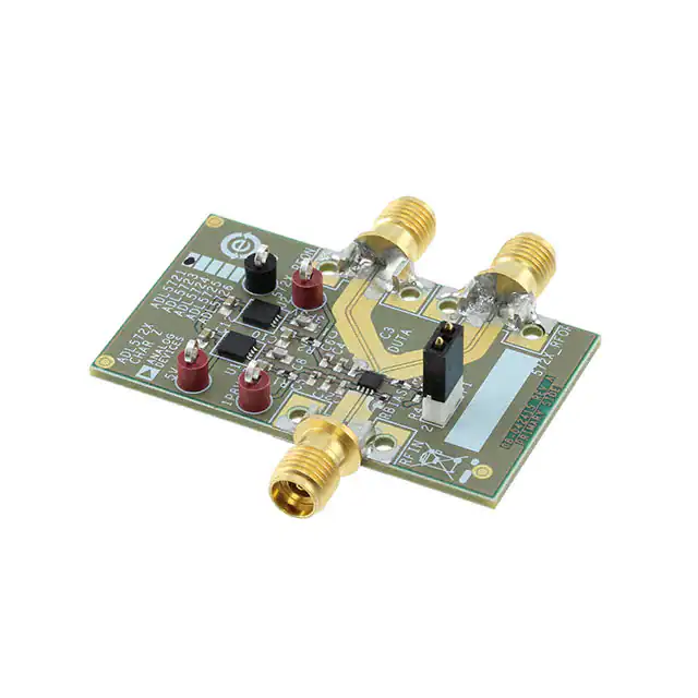
EVALUATION BOARD
20
The ADL5721-EVALZ comes with an ADL5721 chip. It supports
a single 5 V supply for ease of use. For 5 V operation, the 3.3 V
and 1.8 V test loops are for evaluation purposes only. When the
3.3 V and 1.8 V supply is used, remove the R1 and R2 resistors
from the evaluation board. Figure 34 shows a picture of the
ADL5721-EVALZ lab bench setup.
POWER OUTPUT (dBm)
–30
–40
–50
7.16
7.17
7.18
7.19 7.20 7.21 7.22
FREQUENCY (GHz)
7.23
7.24
7.25
14258-036
–80
7.15
Figure 32. Results of the ADL5721 with an Input of 7.2 GHz at −15 dBm,
BAND = 0 V
Power up the ADL5721-EVALZ with a 5 V dc supply. The
supply current of the evaluation board is approximately
88 mA, which is a combination of the VCC1 (1.8 V) and
the VCC2 (3.3 V) currents.
Connect the signal generator to the input of the ADL5721EVALZ.
Connect RFOP and RFON to a 180° hybrid that can work
within the 5.9 GHz to 8.5 GHz frequency range.
Connect the difference output of the hybrid to the spectrum
analyzer. Terminate the sum port of the hybrid to 50 Ω.
Figure 33 shows the results of the differential output for an
input of 8.5 GHz at −15 dBm with a BAND = 1.8 V, with Pin 1
and Pin 2 of the P1 connector open. The hybrid and board loss
were not deembedded.
20
0
See Figure 34 for the ADL5721-EVALZ lab bench setup.
RESULTS
Figure 32 and Figure 33 show the expected results when testing
the ADL5721-EVALZ using the Rev. A version of the evaluation
board and its software. Note that future iterations of the software
may produce different results. See the ADL5721 product page
for the most recent software version.
–10
–20
–30
–40
–50
–60
–80
8.45
8.46
8.47
8.48
8.49 8.50 8.51 8.52
FREQUENCY (GHz)
8.54
8.55
Figure 33. Results of the ADL5721 with an Input of 8.5 GHz at −15 dBm,
BAND = 1.8 V
GND
RFON
SPECTRUM
ANALYZER
INPUT
RFOP
180° HYBRID FOR DIFFERENTIAL
TO SINGLE-ENDED OUTPUT
Figure 34. ADL5721-EVALZ Lab Bench Setup
Rev. 0 | Page 13 of 15
14258-035
RF FREQUENCY GENERATOR
BAND
8.53
14258-037
–70
Figure 32 shows the results of the differential output for an input
of 7.2 GHz at −15 dBm with a BAND = 0 V, with Pin 1 and Pin 2
of the P1 connector shorted. The hybrid and board loss were
not deembedded.
+5V DC
RESOLUTION BANDWIDTH = 20kHz
2
VIDEO BANDWIDTH = 20kHz
10 SWEEP = 301ms (1001pts)
POWER OUTPUT (dBm)
4.
–20
–70
To set up the ADL5721-EVALZ, take the following steps:
3.
–10
–60
INITIAL SETUP
2.
2
0
The band switch feature allows the input P1dB and noise figure
to trade off for optimum system performance. For the lower
frequency band (BAND = 0 V), short Pin 1 and Pin 2 of the
P1 connector. For the higher frequency band (BAND = 1.8 V),
open Pin 1 and Pin 2 of the P1 connector to obtain better
system performance.
1.
RESOLUTION BANDWIDTH = 20kHz
VIDEO BANDWIDTH = 20kHz
10 SWEEP = 301ms (1001pts)
�ADL5721
Data Sheet
BASIC CONNECTIONS FOR OPERATION
Figure 35 shows the basic connections for operating the ADL5721 as it is implemented on the evaluation board of the device.
1.8V
3.3V
C5
0.1UF
C1
4.7NF
AGND
AGND
C2
33PF
C3
33PF
AGND
AGND
C4
4.7NF
C6
0.1UF
AGND
AGND
OUTN
DUTA
1
VCC1
2
GND
3
INPT
4
RBIAS
RFIN
1
25-146-1000-92
CNSRI2516100092_SW109201A5
RFIN
2 3 4
AGND
AGND
8
VCC2
7
OUTN
6
OUTP
5
BAND
572X_RFON
25-146-1000-92
4 3 2
CNSRI2516100092_SW109201A5
AGND
PAD
PAD
ADL5721
RBIAS
442
1
OUTP
AGND
1.8V
1
572X_RFOP
25-146-1000-92
4 3 2 CNSRI2516100092_SW109201A5
AGND
AGND
R4
10K
BAND
5V
RED
1
1
3P3V
RED
1
1P8V
RED
1
GND
BLK
P1
R3
1
2
0
5V
69157-102
3.3V
1.8V
AGND
AGND
U2
U1
ADM7172ACPZ-3.3
R1
0
1
2
C7
4.7UF
AGND
VOUT
VOUT
VIN
VIN
EN
SS
SENSE
EP GND
PAD 6
5V
8
7
5
4
3
3.3V
R2
0
C9
4.7UF
AGND
1
C10
4.7UF
AGND
C8
1000PF
AGND
2
VOUT
VOUT
VIN
VIN
EN
SS
SENSE
EP GND
PAD 6
5V
8
7
5
4
3
C12
4.7UF
AGND
C11
1000PF
AGND
AGND
AGND
14258-034
ADM7170ACPZ-1.8
1.8V
Figure 35. Evaluation Board Schematic
Table 6. Evaluation Board Configuration Options
Component
3P3V, 1P8V, GND, 5V
RFIN, 572X_RFOP, 572x_RFON, BAND
RBIAS
R1, R2
R3
R4
C1 to C12
Function
Power supplies and ground.
Input, output, and data.
442 Ω for RBIAS.
1.8 V and 3.3 V regulator connections.
Band select.
Pull-up or pull-down resistor.
The capacitors provide the required decoupling of the supply
related pins.
P1
U1
U2
DUTA
Jumper to change bands, 2-pin jumper.
ADM7170ACPZ-1.8 1.8 V regulator.
ADM7172ACPZ-3.3 3.3 V regulator.
ADL5721 device under test (DUT).
Rev. 0 | Page 14 of 15
Default Condition
Not applicable
Not applicable
RBIAS = 442 Ω (0402)
R1, R2 = 0 Ω (0402)
R3 = 0 Ω (0603)
R4 = 10 kΩ (0402)
C1, C4 = 4.7 nF (0402),
C2, C3 = 33 pF (0402),
C5, C6 = 0.1 µF (0402),
C7, C9, C10, C12 = 4.7 µF (0603),
C8, C11 = 1000 pF (0603)
Not applicable
Not applicable
Not applicable
Not applicable
�Data Sheet
ADL5721
OUTLINE DIMENSIONS
1.70
1.60
1.50
2.10
2.00 SQ
1.90
0.50 BSC
8
5
1.10
1.00
0.90
EXPOSED
PAD
0.425
0.350
0.275
1
4
TOP VIEW
0.60
0.55
0.50
BOTTOM VIEW
0.05 MAX
0.02 NOM
SEATING
PLANE
0.30
0.25
0.20
PIN 1
INDICATOR
(R 0.15)
FOR PROPER CONNECTION OF
THE EXPOSED PAD, REFER TO
THE PIN CONFIGURATION AND
FUNCTION DESCRIPTIONS
SECTION OF THIS DATA SHEET.
0.20 REF
01-14-2013-C
PIN 1 INDEX
AREA
0.15 REF
Figure 36. 8-Lead Lead Frame Chip Scale Package [LFCSP]
2.00 mm × 2.00 mm Body and 0.55 mm Package Height
(CP-8-10)
Dimensions shown in millimeters
ORDERING GUIDE
Model 1
ADL5721ACPZN
ADL5721ACPZN-R7
ADL5721-EVALZ
1
Temperature Range
−40°C to +85°C
−40°C to +85°C
Package Description
8-Lead Lead Frame Chip Scale Package [LFCSP]
8-Lead Lead Frame Chip Scale Package [LFCSP]
Evaluation Board
Z = RoHS-Compliant Part.
©2016 Analog Devices, Inc. All rights reserved. Trademarks and
registered trademarks are the property of their respective owners.
D14258-0-4/16(0)
Rev. 0 | Page 15 of 15
Package Option
CP-8-10
CP-8-10
�


 工商网监
湘ICP备2023018690号
工商网监
湘ICP备2023018690号
