VMMK-2103
0.5 to 6 GHz Bypass E-pHEMT LNA in Wafer Level Package
Data Sheet
Description
Features
Avago’s VMMK-2103 is an easy-to-use GaAs MMIC bypass
LNA that offers good noise figure and flat gain from 0.5 to
6 GHz in a miniaturized wafer-level package (WLP). The
bias circuit incorporates a power down feature which is
accessed from the input port. This device contains an integrated bypass switch which engages when the amplifier
is in shut down mode, resulting in an improvement in
the input compression point while consuming minimal
current.
• 1 x 0.5 mm Surface Mount Package
The input and output are matched to 50 Ω (better than 2:1
SWR) across the entire bandwidth; no external matching
is needed. This amplifier is fabricated with enhancement
E-pHEMT technology and industry leading wafer level
package. The WLP leadless package is small and ultra thin
yet can be handled and placed with standard 0402 pick
and place assembly.
• Ultrathin (0.25mm)
• LNA Bypass function
• 5V Supply
• RoHS6 + Halogen Free
Specifications (at 3GHz, Vd = Vc = 5V, 23mA Typ.)
• Noise Figure: 2.1dB typical
• Loss in Bypass Mode: 2.3dB
• Associated Gain: 14dB
• Input IP3 in Gain Mode: +8dBm
• Input IP3 in Bypass Mode: +21 dBm
• Input P1dB in Gain Mode: 0dBm
• Input P1dB in Bypass Mode: +17dBm
WLP 0402, 1mm x 0.5mm x 0.25 mm
Applications
• Low Noise and Driver for Cellular/PCS and WCDMA
Base Stations
CY
• 2.4 GHz, 3.5GHz, 5-6GHz WLAN and WiMax notebook
computer, access point and mobile wireless applications
• 802.16 & 802.20 BWA systems
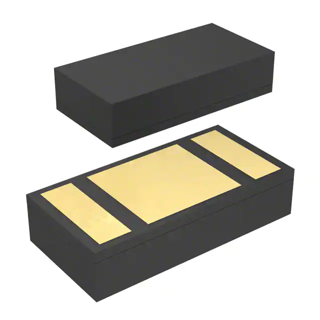
Pin Connections (Top View)
• WLL and MMDS Transceivers
Input
/ Vc
Input
/ Vc
Note:
“C” = Device Code
“Y” = Month Code
CY
Amp
Output
/ Vdd
Output
/ Vdd
• Radar, radio and ECM Systems
Attention: Observe precautions for
handling electrostatic sensitive devices.
ESD Machine Model =50V
ESD Human Body Model =125V
Refer to Avago Application Note A004R:
Electrostatic Discharge, Damage and Control.
�Table 1. Absolute Maximum Ratings [1]
Sym
Parameters/Condition
Unit
Absolute Max
Vd
Supply Voltage (RF Output) [2]
V
8
Vc
Bypass Control Voltage
V
6
Id
Device Current [2]
mA
40
Pin, max
CW RF Input Power (RF Input) [3]
dBm
+20
Pdiss
Total Power Dissipation
mW
320
Tch
Max channel temperature
°C
150
Θjc
Thermal Resistance [4]
°C/W
110
Notes
1. Operation in excess of any of these conditions may result in permanent damage to this device.
2. Bias is assumed DC quiescent conditions
3. With the DC (typical bias in both modes) and RF applied to the device at board temperature Tb = 25°C
4. Thermal resistance is measured from junction to board using IR method
Table 2. DC and RF Specifications
TA= 25°C, Frequency = 3 GHz, Vd = 5V, Vc=5V, Zin=Zout=50Ω (unless otherwise specified)
Sym
Parameters/Condition
Unit
Minimum
Typ.
Maximum
Id
Device Current
mA
16
23
30
Id_leakage [6]
Current in Bypass Mode
mA
0.6
1.5
NF[1]
Noise Figure
dB
–
2.1
2.7
Ga [1]
Associated Gain
dB
12
14
16
Ga_Bypass [1,6]
Associated Gain in Bypass Mode
dB
-4.1
-2.3
IIP3_Gain [2,3]
Input IP3 in Gain Mode
dBm
8
IIP3_Bypass[ 2,4,6]
Input IP3 in Bypass Mode
dBm
21
IP1dB_Gain [2]
Input P1dB in Gain Mode
dBm
0
IP1dB_Bypass [2,6]
Input P-1dB in Bypass Mode
IRL [2]
Input Return Loss
dB
–
-11
–
ORL [2]
Output Return Loss
dB
–
-13
–
ts [5]
Switching Time
µs
17
0.1
Notes:
1. Measure data obtained using 300um G-S production wafer probe
2. Measure data obtained using 300um G-S-G PCB probe on substrate
3. IIP3 test condition: F1 = 3.0GHz, F2 = 3.01GHz, Pin = -10dBm in Gain Mode for typical performance during characterization
4. IIP3 test condition: F1 = 3.0GHz, F2 = 3.01GHz, Pin = 0dBm in Bypass Mode for typical performance during characterization
5. Switching time measured using test board (Figure 20)
6. Bypass Mode Bias Voltages are Vd = 5V, Vc = 0V
2
–
�Product Consistency Distribution Charts at 3.0 GHz, Vd = 5V, Vc = 5V
LSL
.016
USL
.018
.02
.022
.024
.026
.028
.03
Id @ Vd=Vc=5V, Mean=23mA, LSL=16mA, USL=30mA
USL
13
14
0
USL
.0002
.0005
.0008
15
16
Gain @ 3 GHz, Mean=14dB , LSL=12dB, USL=16dB
1.9
2
2.1
2.2
2.3
2.4
-4
-3
Bypass Gain @ 3 GHz, Mean=-2.3dB, LSL=-4.1dB
2.5
2.6
2.7
NF @ 3 GHz, Mean=2.1dB , USL=2.7dB
Notes:
Distribution data based on 500 part sample size from 3 lots during initial characterization.
Measurements were obtained using 300um G-S production wafer probe.
Future wafers allocated to this product may have nominal values anywhere between the upper and lower limits.
3
.0012
LSL
USL
1.8
.001
Id_bypass @Vd=5V, Vc=0V, Mean=0.6mA, USL=1.5mA
LSL
12
LSL
-2
.0015
�VMMK-2103 Typical Performance
(TA = 25°C, Zin = Zout = 50 Ω unless noted)
20
3
2
10
NF (dB)
S21 (dB)
15
Vd=5V, Vc=5V
Vd=5V, Vc=0V
5
1
0
-5
Vd=5V, Vc=5V
Vd=5V, Vc=0V
0
1
2
3
4
Freq (GHz)
5
6
0
7
Figure 1. Small-signal Gain [1]
6
7
-5
S22 (dB)
S11 (dB)
5
Vd=5V, Vc=5V
Vd=5V, Vc=0V
-10
-10
-15
0
1
2
3
4
Freq (GHz)
5
6
-20
7
Figure 3. Input Return Loss [1]
0
1
2
3
4
Freq (GHz)
5
25
-5
20
-10
Input IP3 (dBm)
0
Vd=5V, Vc=5V
Vd=5V, Vc=0V
-15
1
Figure 5. Isolation [1]
2
7
15
10
5
0
6
Figure 4. Output Return Loss [1]
-20
3
4
Freq (GHz)
5
6
7
0
Vd=5V, Vc=5V
Vd=5V, Vc=0V
2
3
4
5
Freq (GHz)
Figure 6. Input Third Order Intercept Point [1,2]
Notes:
1. Data taken on a G-S-G probe substrate fully de-embedded to the reference plane of the package
2. Input IP3 data for bypass mode (Vc=0V) taken at Pin=0dBm; for gain mode, Pin=-15dBm
4
3
4
Freq (GHz)
0
-15
S12 (dB)
2
Vd=5V, Vc=5V
Vd=5V, Vc=0V
-5
-25
1
Figure 2. Noise Figure [1]
0
-20
0
6
7
�VMMK-2103 Typical Performance (continue)
(TA = 25°C, Zin = Zout = 50 Ω unless noted)
25
30
15
20
Id (mA)
Input P1dB (dBm)
20
Vd=5V, Vc=5V
Vd=5V, Vc=0V
10
5
10
0
-5
1
2
3
4
Freq (GHz)
5
6
0
7
Figure 7. Input Power at 1dB Gain Compression [1]
0
1
2
3
Vd (V)
4
5
6
Figure 8. Total Current at Vc = 5V [1]
3
20
2
10
NF (dB)
S21 (dB)
15
Vd=5V, Vc=5V
Vd=3V, Vc=3V
Vd=5V, Vc=0V
Vd=3V, Vc=0V
5
1
0
-5
Vd=Vc=5V
Vd=Vc=3V
0
1
2
3
Freq (GHz)
4
5
6
0
7
Figure 9. Gain Over Vdd [1]
2
-15
5
6
7
5
6
7
-10
-15
0
1
2
3
4
Freq (GHz)
Figure 11. Input Return Loss over Vdd [1]
5
6
7
-20
0
1
2
3
4
Freq (GHz)
Figure 12. Output Return Loss Over Vdd [1]
Notes:
1. Data taken on a G-S-G probe substrate fully de-embedded to the reference plane of the package
5
3
4
Freq (GHz)
Vd=5V, Vc=5V
Vd=3V, Vc=3V
Vd=5V, Vc=0V
Vd=3V, Vc=0V
-5
S22 (dB)
S11 (dB)
0
Vd=5V, Vc=5V
Vd=3V, Vc=3V
Vd=5V, Vc=0V
Vd=3V, Vc=0V
-10
-20
1
Figure 10 Noise Figure over Vdd [1]
0
-5
0
�VMMK-2103 Typical Performance (continue)
5
15
0
10
Input IP3 (dBm)
Input P1dB (dBm)
(TA = 25°C, Zin = Zout = 50 Ω unless noted)
-5
5
Vd=5V, Vc=5V
Vd=3V, Vc=3V
Vd=5V, Vc=5V
Vd=3V, Vc=3V
-10
2
3
4
5
6
0
7
2
3
4
5
6
7
Freq (GHz)
Freq (GHz)
Figure 13. Input P1dB over Vdd in Gain Mode [1]
Figure 14. Input IP3 Over Vdd in Gain Mode [1,2]
20
3
15
2
25C Gain
25C Bypass
5
-40C Gain
-40C Bypass
NF (dB)
S21 (dB)
10
85CGain
85C Bypass
0
1
25C
-40C
85C
-5
-10
1
2
3
4
Freq (GHz)
5
6
0
7
Figure 15. Gain over Temp [3]
3
5
6
7
15
0
-5
5
25C
-40C
85C
2
3
4
5
6
10
7
0
25C
-40C
85C
1
2
Freq (GHz)
Figure 17. Input P1dB Over Temp in Gain Mode [3]
3
4
Freq (GHz)
Figure 18. Input IP3 Over Temp in Gain Mode [2,3]
Notes:
1. Data taken on a G-S-G probe substrate fully de-embedded to the reference plane of the package
2. Input IP3 data for bypass mode (Vc=0V) taken at Pin=0dBm; for gain mode, Pin=-15dBm
3. Over temp data taken on a test fixture (Figure 20) without de-embedding
6
4
Freq (GHz)
20
IIP3 (dBm)
Input P1dB (dBm)
2
Figure 16 Noise Figure over Temp [3]
5
-10
1
5
6
7
�VMMK-2103 Typical S-parameters in Gain State
(Data obtained using 300um G-S-G PCB substrate, losses calibrated out to the package reference plane;
TA = 25°C, Vdd=5V, Vc=5V, Idd=23mA, Zin = Zout = 50 Ω unless noted)
7
Freq
GHz
S11
S21
S12
S22
dB
Mag
Phase
dB
Mag
Phase
dB
Mag
Phase
dB
Mag
Phase
0.1
-8.876
0.360
-50.581
16.829
6.942
176.611
-19.494
0.106
5.108
-9.404
0.339
-55.085
0.2
-12.270
0.244
-36.591
16.319
6.546
172.477
-19.584
0.105
0.002
-13.850
0.203
-43.101
0.3
-12.887
0.227
-30.174
16.117
6.395
169.661
-19.551
0.105
-3.117
-15.427
0.169
-33.218
0.4
-12.910
0.226
-28.995
16.006
6.314
167.231
-19.626
0.104
-4.633
-16.071
0.157
-26.579
0.5
-12.608
0.234
-21.522
15.848
6.200
168.339
-19.601
0.105
-3.401
-15.746
0.163
-10.589
0.9
-12.234
0.245
-31.690
15.684
6.084
161.128
-19.668
0.104
-7.506
-15.504
0.168
-3.349
1
-12.164
0.247
-34.073
15.658
6.066
159.287
-19.651
0.104
-8.499
-15.406
0.170
-2.282
1.5
-11.989
0.252
-49.198
15.480
5.943
150.058
-19.752
0.103
-13.093
-14.890
0.180
0.197
2
-11.839
0.256
-63.764
15.263
5.796
140.942
-19.845
0.102
-17.609
-14.329
0.192
0.774
2.5
-11.684
0.261
-77.546
15.033
5.645
132.079
-19.914
0.101
-22.064
-13.748
0.205
0.477
3
-11.535
0.265
-91.848
14.756
5.468
123.472
-20.052
0.099
-26.489
-13.124
0.221
0.527
3.5
-11.366
0.270
-103.974
14.488
5.301
115.038
-20.184
0.098
-31.117
-12.586
0.235
-1.231
4
-11.119
0.278
-115.567
14.209
5.134
106.819
-20.291
0.097
-35.608
-11.938
0.253
-4.965
4.5
-10.818
0.288
-126.554
13.943
4.979
98.880
-20.473
0.095
-40.251
-11.337
0.271
-8.749
5
-10.562
0.296
-137.192
13.658
4.818
90.999
-20.677
0.093
-44.626
-10.737
0.291
-12.668
5.5
-10.323
0.305
-146.916
13.380
4.667
83.237
-20.896
0.090
-49.245
-10.190
0.309
-17.172
6
-10.017
0.316
-156.605
13.113
4.525
75.640
-21.130
0.088
-54.220
-9.653
0.329
-21.621
6.5
-9.730
0.326
-166.084
12.844
4.387
68.093
-21.432
0.085
-58.831
-9.121
0.350
-26.308
7
-9.427
0.338
-175.142
12.580
4.256
60.663
-21.692
0.082
-63.579
-8.650
0.369
-31.224
7.5
-9.091
0.351
176.177
12.311
4.126
53.307
-22.047
0.079
-68.271
-8.210
0.389
-36.074
8
-8.745
0.365
167.300
12.054
4.006
45.851
-22.372
0.076
-73.024
-7.763
0.409
-41.086
8.5
-8.443
0.378
159.051
11.786
3.884
38.662
-22.745
0.073
-77.870
-7.333
0.430
-46.100
9
-8.070
0.395
150.995
11.524
3.769
31.423
-23.198
0.069
-83.171
-6.930
0.450
-51.449
9.5
-7.689
0.413
142.602
11.262
3.657
24.176
-23.649
0.066
-87.948
-6.575
0.469
-56.356
10
-7.329
0.430
134.912
10.992
3.545
16.891
-24.138
0.062
-93.302
-6.162
0.492
-61.479
10.5
-6.922
0.451
127.167
10.724
3.437
9.738
-24.642
0.059
-98.766
-5.833
0.511
-66.707
11
-6.549
0.471
119.700
10.449
3.330
2.475
-25.288
0.054
-104.531
-5.479
0.532
-71.957
11.5
-6.168
0.492
112.078
10.158
3.220
-4.775
-25.849
0.051
-110.478
-5.150
0.553
-77.110
12
-5.811
0.512
105.112
9.865
3.114
-11.968
-26.614
0.047
-115.827
-4.808
0.575
-82.407
12.5
-5.451
0.534
97.806
9.555
3.004
-19.144
-27.412
0.043
-121.940
-4.485
0.597
-87.740
13
-5.069
0.558
91.034
9.234
2.895
-26.308
-28.179
0.039
-128.028
-4.203
0.616
-92.835
13.5
-4.728
0.580
84.198
8.903
2.787
-33.415
-29.119
0.035
-135.270
-3.900
0.638
-98.017
14
-4.401
0.603
77.730
8.567
2.681
-40.569
-30.257
0.031
-143.074
-3.612
0.660
-103.148
�VMMK-2103 Typical S-parameters in Bypass State
(Data obtained using 300um G-S-G PCB substrate, losses calibrated out to the package reference plane;
TA = 25°C, Vdd=5V, Vc=0V, Idd=0.6mA, Zin = Zout = 50 Ω unless noted)
8
Freq
GHz
S11
S21
S12
S22
dB
Mag
Phase
dB
Mag
Phase
dB
Mag
Phase
dB
Mag
Phase
0.1
-1.783
0.814
-28.679
-7.459
0.424
52.470
-7.488
0.422
52.351
-1.575
0.834
-26.461
0.2
-4.424
0.601
-42.034
-4.305
0.609
32.344
-4.329
0.608
32.536
-3.997
0.631
-39.454
0.3
-6.577
0.469
-46.955
-3.340
0.681
20.626
-3.359
0.679
20.936
-6.048
0.498
-44.552
0.4
-8.154
0.391
-48.467
-2.944
0.713
13.113
-2.952
0.712
13.388
-7.570
0.418
-46.186
0.5
-9.319
0.342
-44.468
-2.796
0.725
11.152
-2.796
0.725
11.316
-8.683
0.368
-42.316
0.9
-11.647
0.262
-42.225
-2.525
0.748
0.119
-2.534
0.747
0.318
-10.958
0.283
-39.530
1
-11.938
0.253
-41.789
-2.509
0.749
-1.784
-2.510
0.749
-1.634
-11.239
0.274
-38.886
1.5
-12.857
0.228
-43.145
-2.491
0.751
-9.483
-2.499
0.750
-9.319
-12.048
0.250
-39.139
2
-13.291
0.217
-46.787
-2.508
0.749
-15.778
-2.516
0.749
-15.569
-12.367
0.241
-41.755
2.5
-13.510
0.211
-51.914
-2.534
0.747
-21.385
-2.542
0.746
-21.281
-12.472
0.238
-45.429
3
-13.786
0.205
-58.267
-2.592
0.742
-26.797
-2.598
0.742
-26.724
-12.672
0.233
-50.016
3.5
-14.005
0.199
-64.423
-2.613
0.740
-32.019
-2.627
0.739
-31.925
-12.642
0.233
-55.405
4
-14.093
0.197
-71.644
-2.654
0.737
-37.161
-2.665
0.736
-37.053
-12.479
0.238
-59.927
4.5
-14.137
0.196
-79.054
-2.679
0.735
-42.193
-2.683
0.734
-42.150
-12.281
0.243
-64.996
5
-14.280
0.193
-87.252
-2.720
0.731
-47.296
-2.726
0.731
-47.196
-12.083
0.249
-70.218
5.5
-14.452
0.189
-95.034
-2.766
0.727
-52.335
-2.766
0.727
-52.294
-11.873
0.255
-75.476
6
-14.462
0.189
-103.880
-2.804
0.724
-57.423
-2.811
0.724
-57.354
-11.617
0.263
-80.534
6.5
-14.559
0.187
-113.166
-2.847
0.721
-62.558
-2.858
0.720
-62.499
-11.360
0.270
-85.294
7
-14.572
0.187
-122.733
-2.897
0.716
-67.739
-2.899
0.716
-67.657
-11.054
0.280
-90.818
7.5
-14.531
0.188
-132.794
-2.948
0.712
-72.905
-2.959
0.711
-72.847
-10.815
0.288
-95.990
8
-14.466
0.189
-143.549
-3.004
0.708
-78.235
-3.017
0.707
-78.118
-10.487
0.299
-101.093
8.5
-14.348
0.192
-153.759
-3.073
0.702
-83.500
-3.077
0.702
-83.352
-10.192
0.309
-106.034
9
-13.992
0.200
-164.621
-3.135
0.697
-88.876
-3.138
0.697
-88.811
-9.797
0.324
-111.230
9.5
-13.664
0.207
-176.432
-3.224
0.690
-94.404
-3.222
0.690
-94.284
-9.549
0.333
-116.425
10
-13.207
0.219
172.707
-3.305
0.684
-99.915
-3.301
0.684
-99.852
-9.196
0.347
-121.210
10.5
-12.631
0.234
161.575
-3.402
0.676
-105.528
-3.397
0.676
-105.465
-8.888
0.359
-126.564
11
-12.010
0.251
151.115
-3.510
0.668
-111.272
-3.501
0.668
-111.257
-8.573
0.373
-131.771
11.5
-11.415
0.269
140.472
-3.629
0.659
-117.082
-3.629
0.659
-117.046
-8.266
0.386
-136.822
12
-10.719
0.291
131.006
-3.768
0.648
-122.942
-3.773
0.648
-122.934
-7.946
0.401
-142.091
12.5
-10.072
0.314
121.223
-3.919
0.637
-128.970
-3.931
0.636
-128.910
-7.614
0.416
-147.433
13
-9.358
0.341
112.238
-4.096
0.624
-134.946
-4.105
0.623
-134.873
-7.383
0.427
-152.688
13.5
-8.678
0.368
103.491
-4.291
0.610
-141.009
-4.308
0.609
-140.922
-7.117
0.441
-157.942
14
-8.020
0.397
95.355
-4.501
0.596
-147.240
-4.521
0.594
-146.997
-6.878
0.453
-163.398
�VMMK-2103 Application and Usage
(Please always refer to the latest Application Note AN5378 in website)
Biasing and Operation
The VMMK-2103 can be used as a low noise amplifier or as a
driver amplifier. The nominal bias condition for the VMMK2103 is Vd = Vc = 5V. At this bias condition, the device provides
an optimal compromise between power consumption, noise
figure, gain, power output, and OIP3. The VMMK-2103 is
biased with a positive supply connected to the output pin Vd
through an external user supplied bias decoupling network
as shown in Figure 19. A control voltage Vc is applied to
the input pin through a similar bias decoupling network.
The VMMK-2103 operates in the gain mode when Vc=Vd.
Nominal Vd is between 3 and 5 V. When Vc is at 0V, the device
is biased in the “bypass” mode, which engages the integrated
bypass switch which then shuts down the amplifier.
Vc
Vdd
0.1 uF
0.1 uF
100 pF
22 nH
15 nH
Input
Output
Amp
100 pF
Input
Pad
50 Ohm line
Ground
Pad
Output
Pad
100 pF
50 Ohm line
Figure 19. Example application of VMMK-2103 at 3GHz
The output bias decoupling network can be easily constructed using small surface mount components. The value
of the output inductor can have a major effect on both
low and high frequency operation. The demo board uses
a 15 nH inductor that has a self resonant frequency higher
than the maximum desired frequency of operation. If the
self-resonant frequency of the inductor is too close to the
operating band, the value of the inductor will need to be
adjusted so that the self-resonant frequency is significantly
higher than the highest frequency of operation.
Typically a passive component company like Murata does
not specify S parameters at frequencies higher than 5 or
6 GHz for larger values of inductance making it difficult
to properly simulate amplifier performance at higher
frequencies. It has been observed that the Murata LQW15AN
series of 0402 inductors actually works quite well above their
normally specified frequency. As an example, increasing the
output inductor from 15 nH to 39 nH provides bandwidth
from 200 MHz through 6 GHz with good gain flatness.
Further extending the low frequency response of the VMMK2103 is possible by using two different value inductors in
series with the smaller value inductor placed closest to the
device and favoring the higher frequencies. The larger value
inductor will then offer better low frequency performance by
not loading the output of the device.
9
Figure 20. Evaluation/Test Board (available to qualified customer request)
The parallel combination of the 100pF and 0.1uF capacitors
provide a low impedance in the band of operation and at
lower frequencies and should be placed as close as possible
to the inductor. The low frequency bypass provides good
rejection of power supply noise and also provides a low
impedance termination for third order low frequency mixing
products that will be generated when multiple in-band
signals are injected into any amplifier.
The input bias decoupling network is similar to that used on
the output. A 22 nH inductor bypass with a 100pF capacitor
provides a means to control Vc on the input port. Since there
is a voltage developed internally to the VMMK-2103 at the
input terminal, any resistance in series with the power supply
will actually raise the input terminal above ground enough
that it begins to affect linearity in the bypass mode. Switching
time between the gain mode and the bypass mode is under
0.1 µsec. If switching speed is not a high priority, then the
bypass capacitor on the input should be raised to 0.1 uF to
help minimize noise and spurious from the power supply
adversely affecting the operation of the VMMK-2103.
S Parameter Measurements
The S-parameters are measured on a .016 inch thick RO4003
printed circuit test board, using G-S-G (ground signal
ground) probes. Coplanar waveguide is used to provide a
smooth transition from the probes to the device under test.
The presence of the ground plane on top of the test board
results in excellent grounding at the device under test. A
combination of SOLT (Short - Open - Load - Thru) and TRL
(Thru - Reflect - Line) calibration techniques are used to
correct for the effects of the test board, resulting in accurate
device S-parameters. The reference plane for the S Parameters is at the edge of the package.
The product consistency distribution charts shown on
page 2 represent data taken by the production wafer probe
station using a 300um G-S wafer probe. The ground-signal
probing that is used in production allows the device to be
probed directly at the device with minimal common lead
inductance to ground. Therefore there will be a slight difference in the nominal gain obtained at the test frequency
using the 300um G-S wafer probe versus the 300um G-S-G
printed circuit board substrate method.
�fy the device
rial with one
tal. Soldering
ion than FR5
materials with
e of the base
evice circuitry
GaAs package
to damaging
RO4003 and
al and should
g
source leads
leads of the
unt. The recern is shown
ned footprint
t borders the
en.
re any plated
ng and tests
in .003”) and
re 5 provides
VMMK-3XXX
ness RO4350
e also applies
t frequencies
-1XXX FETs at
ductance may
may be placed
bility. Consult
ation.
of the VMMK
that the VIAs
om under the
of the VIAs is
e VIAs should
Outline Drawing
1.004 MIN, 1.085 MAX
PIN ONE INDICATOR
0.125
0.125
GROUND PAD
0.500 MIN, 0.585 MAX
0.470
OUTPUT PAD
0.390
0.160
INPUT PAD
0.160
Notes:
Solderable area of the device shown in yellow.
Dimensions in mm.
Tolerance ± 0.015mm
Suggested PCB Material and Land Pattern
Recommended SMT Attachment
The VMMK Packaged Devices are compatible with high
volume surface mount PCB assembly processes.
1.2 (0.048)
0.400 (0.016)
0.100 (0.004)
0.076 max
(0.003) 2pl see discussion
0.381 (0.015) 2pl
1. Follow ESD precautions while handling packages.
0.100 (0.004)
0.500 (0.020)
Part of
Input
Circuit
Manual Assembly for Prototypes
2. Handling should be along the edges with tweezers or
from topside if using a vacuum collet.
0.500 (0.020)
0.200
(0.008)
Part of
Output
Circuit
0.200
(0.008)
0.7 (0.028)
0.254 dia PTH
(0.010) 4pl
Solder Mask
0.400 dia
(0.016) 4pl
Figure 5. Recommended PCB layout for VMMK devices
Notes:
1. 0.010” Rogers RO4350
As a general rule, if a VIA is within .004” (100u) of the edge
of the soldermask but not under the device, then the VIA
should be filled. Any VIA which is covered by the solder
mask and is beyond .004” (100u) of the solder mask edge
can be uncapped and unfilled as it is not at risk of wicking
away solder from the device.
If for any reason it is required to include a VIA or VIAs
under a VMMK device, then the VIAs should be filled and
capped. A capped VIA is a “plated over” filled VIA. If a filled
but uncapped VIA is placed under the device, there will
not be enough solderable surface area for device attachment. If an unfilled and uncapped VIA is placed directly
under the ground pad, then the liquid solder will flow
into the open VIA hole during the reflow process and
deplete the solder volume to varying degrees from
under the ground pad. Depletion of the solder volume
10
due to unfilled VIAs may lead to a weak solder joint, poor
grounding of the device, and/or stresses compromising
the structural integrity of the package.
3. Recommended attachment is solder paste. Please
see recommended solder reflow profile. Conductive
epoxy is not recommended. Hand soldering is not
recommended.
4. Apply solder paste using either a stencil printer or dot
placement. The volume of solder paste will be dependent on PCB and component layout and should be
controlled to ensure consistent mechanical and electrical performance. Excessive solder will degrade RF performance.
5. Follow solder paste and vendor’s recommendations
when developing a solder reflow profile. A standard
profile will have a steady ramp up from room temperature to the pre-heat temp to avoid damage due to
thermal shock.
6. Packages have been qualified to withstand a peak temperature of 260°C for 20 to 40 sec. Verify that the profile
will not expose device beyond these limits.
7. Clean off flux per vendor’s recommendations.
8. Clean the module with Acetone. Rinse with alcohol.
Allow the module to dry before testing.
�Ordering Information
Part Number
Devices Per
Container
Container
VMMK-2103-BLKG
100
Antistatic Bag
VMMK-2103-TR1G
5000
7” Reel
Package Dimension Outline
D
Die dimension:
E
A
Dim
Range
Unit
D
1.004 - 1.085
mm
E
0.500 - 0.585
mm
A
0.225 - 0.275
mm
Note:
All dimensions are in mm
Reel Orientation
Device Orientation
REEL
USER FEED DIRECTION
4 mm
TOP VIEW
Note:
“C” = Device Code
”Y” = Month Code
•CY
•CY
11
CARRIER
TAPE
•CY
•CY
USER
FEED
DIRECTION
8 mm
END VIEW
�Tape Dimensions
T
Do
Note: 1
Po
B
A
A
P1
Scale 5:1
Bo
W
Note: 2
F
E
5° (Max)
B
D1
B–B SECTION
Note: 2
P2
Ao
R0.1
5° (Max)
Ko
Ao = 0.73±0.05 mm
Scale 5:1
Bo = 1.26±0.05 mm
A–A SECTION
mm
Ko = 0.35 +0.05
+0
Unit: mm
Symbol
K1
Po
P1
P2
Do
D1
E
F
10Po
W
T
Unit: mm
Spec.
–Symbol
K1
4.0±0.10
Po
4.0±0.10
P1
2.0±0.05
P2
1.55±0.05
Do
0.5±0.05
D1
1.75±0.10
E
3.50±0.05
F
40.0±0.10
10Po
8.0±0.20
W
0.20±0.02
T
Notice:
1. 10 Sprocket hole pitch cumulative tolerance is ±0.1mm.
2. Pocket position relative to sprocket hole measured as true position of pocket not pocket hole.
Notice:
Spec. 3. Ao & Bo measured on a place
0.3mm above the bottom of the pocket to top surface of the carrier.
1. 10 Sprocket hole pitch cumulative tolerance is ±0.1mm.
4. Ko measured from a plane on the inside bottom of the pocket to the top surface of the carrier.
–
2. Pocket position relative to sprocket hole measured as true position
5. Carrier camber shall be not than 1m per 100mm through a length of 250mm.
of pocket not pocket hole.
4.0±0.10
3. Ao & Bo measured on a place 0.3mm above the bottom of the
4.0±0.10
pocket to top surface of the carrier.
2.0±0.05
4. Ko measured from a plane on the inside bottom of the pocket to
the top surface of the carrier.
1.55±0.05
5. Carrier camber shall be not than 1m per 100mm through a length
0.5±0.05
of 250mm.
1.75±0.10
3.50±0.05
40.0±0.10
8.0±0.20
0.20±0.02
For product information and a complete list of distributors, please go to our web site:
www.avagotech.com
Avago, Avago Technologies, and the A logo are trademarks of Avago Technologies in the United States and other countries.
Data subject to change. Copyright © 2005-2013 Avago Technologies. All rights reserved.
AV02-2000EN - December 6, 2013
�