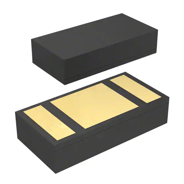
VMMK-3603
1 - 6 GHz Positive Gain Slope Low Noise Amplifier in SMT Package
Data Sheet
Description
Features
The VMMK-3603 is a small and easy-to-use, broadband,
positive gain slope low noise amplifier operating in various
frequency bands from 1 to 6 GHz with typical noise figure
of 1.4 dB. It is housed in the Avago Technologies’ industryleading and revolutionary sub-miniature chip scale
package (GaAsCap wafer scale leadless package) which is
small and ultra thin yet can be handled and placed with
standard 0402 pick and place assembly equipment. The
VMMK-3603 provides a typical gain of 17 dB with good
linearity of +25 dBm typical OIP3 and input and output
return losses. It can be operated from 3 V to 5 V power
supply. It is fabricated using Avago Technologies unique
0.25 μm E-mode PHEMT technology which eliminates the
need for negative gate biasing voltage.
• 1 x 0.5 mm surface mount package
WLP0402, 1 mm x 0.5 mm x 0.25 mm
Applications
• Ultrathin (0.25 mm)
• Wide frequency range: 1 to 6 GHz
• Low noise figure
• Positive gain slope
• Self-Biasing: 3 to 5 V
Specifications (5 GHz, Vdd = 5 V, Zin = Zout = 50 Ω)
• Small signal gain: 17 dB typ.
• Noise Figure = 1.5 dB typ.
• Output 3rd Order Intercept Point = 25 dBm
• 2.4, 3.5, and 5-6 GHz WLAN and WiMax
• 802.16 & 802.20 BWA systems
MY
• Radar and ECM systems
• Generic IF amplifier
Pin Connections (Top View)
Input
Input
Note:
“M” = Device Code
“Y” = Month Code
MY
Amp
Output
Output
Attention: Observe precautions for
handling electrostatic sensitive devices.
ESD Machine Model = 50 V
ESD Human Body Model = 300 V
Refer to Avago Application Note A004R:
Electrostatic Discharge, Damage and Control.
�Electrical Specifications
Table 1. Absolute Maximum Rating [1]
Symbol
Parameters/Condition
Unit
Absolute Max
Vd
Supply Voltage (RF Output) [2]
V
8
Id
Supply Current [2]
mA
56
Pin, max
CW RF Input Power (RF Input) [3]
dBm
15
Pdiss
Total Power Dissipation
mW
460
Tch
Max Channel Temperature
°C
+150
θjc
Thermal Resistance [4]
°C/W
95.3
Notes
1. Operation of this device above any one of these parameters may cause permanent damage
2. Bias is assumed DC quiescent conditions
3. With the DC (typical bias) and RF applied to the device at board temperature Tb = 25° C
4. Thermal resistance is measured from junction to board using IR method
Table 2. DC and RF Specifications [1]
TA = 25° C, Vd = 5 V, Freq = 5 GHz, Zin = Zout = 50 Ω (unless otherwise specified)
Symbol
Parameters/Condition
Unit
Minimum
Typical
Maximum
Id [2]
Supply Current
mA
27
36
44
NF [2,3]
Noise Figure
dB
1.5
1.9
Ga [2,3]
Associated Gain
dB
16.8
19.5
S11 [4]
Input Return Loss
dB
-11
S22 [4]
Output Return Loss
dB
-11
OIP3 [4,5]
Output 3rd Order Intercept Point
dBm
25
Notes
1. Losses of the test system have been de-embedded from final data
2. Measured data obtained from wafer-probing using a G-S, S-G pyramid probe
3. NF and Ga obtained from Noise Figure Meter
4. S-parameters and OIP3 data obtained using 300 mm G-S-G probing on PCB substrate
5. OIP3 test condition: Center frequency = 5 GHz, 2 tone offset = 10 MHz, Pin = -25 dBm
2
15.5
�Product Consistency Distribution Charts at 5.0 GHz, Vd = 5 V
LSL
0.023
USL
USL
0.025
0.032
0.036
0.04
0.044
0.048
Id @ Vd = 5 V, Mean = 36 mA, LSL = 27 mA, USL = 44mA
0.9
1
1.1
1.3
1.5
1.7
1.9
2
2.1
NF @ 5 GHz, Mean = 1.5 dB, USL = 1.9 dB
LSL
USL
Notes:
Distribution data based on 65 Kpcs part sample size from MPV lots.
Future wafers allocated to this product may have nominal values
anywhere between the upper and lower limits.
15
16
17
18
19
Gain @ 5GHz, Mean = 16.8 dB, LSL = 15.5 dB, USL = 19.5 dB
(Data obtained using Noise Figure Analyzer)
3
20
�VMMK-3603 Typical Performance
TA = 25° C, Zin = Zout = 50 Ω; biasing by a broadband bias tee; S-param data obtained using 300 mm GSG probing on PCB
substrate, NF, IP3, and P1dB obtained using eval board; losses calibrated out to the package reference plane.
0.0
21.0
18.0
-3.0
12.0
S11 (dB)
S21 (dB)
15.0
9.0
6.0
3V
4V
5V
3.0
0.0
0
1
2
3
4
5
6
Frequency (GHz)
7
8
9
10
-15.0
0
1
2
3
4
5
6
Frequency (GHz)
7
8
1.6
1.4
1.2
3V
4V
5V
0
1
2
3
4
5
6
Frequency (GHz)
7
8
9
1
0.8
10
3V
5V
0
1
2
3
4
Frequency (GHz)
5
6
7
Figure 4. NF Over Bias
25
13
P1dB (dBm)
16
20
15
10
7
3V
5V
1
3V
5V
2
Figure 5. OIP3 Over Bias
4
10
1.8
30
10
9
2
NF (dB)
S22 (dB)
3V
4V
5V
Figure 2. Input Return Loss Over Bias
Figure 3. Output Return Loss Over Bias
OIP3 (dBm)
-9.0
-12.0
Figure 1. Small Signal Gain Over Bias
0.0
-3.0
-6.0
-9.0
-12.0
-15.0
-18.0
-21.0
-24.0
-27.0
-30.0
-6.0
3
4
Frequency (GHz)
5
6
4
1
2
Figure 6. OP1dB Over Bias
3
4
Frequency (GHz)
5
6
�VMMK-3603 Typical Performance
Vd = 5 V unless noted, Zin = Zout = 50 Ω, biasing by a broadband bias tee; over temp data obtained using eval board;
losses calibrated out to the package reference plane.
18
45
40
17
30
S21(dB)
Id (mA)
35
25
20
10
15
25° C
-40° C
+85° C
15
2
3
4
Vd (Volts)
5
16
14
6
Figure 7. Id vs. Vd over Temp
25° C
-40° C
+85° C
1
2
3
4
Frequency (GHz)
5
6
Figure 8. Gain over Temp
2.2
35
2
30
1.8
OIP3 (dBm)
NF (dB)
1.6
1.4
1.2
1
20
25° C
-35° C
+85° C
0.8
0.6
0
1
2
3
4
Frequency (GHz)
5
6
7
Figure 9. NF Over Temp
P1dB (dBm)
13
10
7
25° C
-40° C
+85° C
1
2
Figure 11. OP1dB Over Temp
5
15
25° C
-40° C
+85° C
1
2
Figure10. OIP3 Over Temp
16
4
25
3
4
Frequency (GHz)
5
6
3
4
Frequency (GHz)
5
6
�Typical Scattering Parameters
TA = 25° C, Vd = 3 V, Zin = Zout = 50 Ω unless noted. Data obtained using 300 mm G-S-G PCB substrate & broadband bias
tees, losses calibrated out to the package reference plane.
Freq
GHz
S11
dB
mag
Phase
dB
mag
phase
dB
mag
phase
dB
mag
Phase
0.05
-0.2
0.977
-4.8864
19.2
9.153
-179.6516
-38.2
0.0123
91.3266
-7.7
0.4127
0.6165
0.1
-0.3
0.9706
-9.9273
19.3
9.2677
176.9829
-35.4
0.0169
75.7197
-7.3
0.431
-6.0822
0.2
-0.6
0.931
-19.6121
19.2
9.1431
170.3651
-30.1
0.0312
66.652
-7.4
0.4254
-17.5835
0.3
-1.2
0.8726
-28.1505
18.9
8.8217
165.3938
-27.3
0.0432
57.1804
-8.0
0.3971
-27.3636
0.4
-1.8
0.8098
-35.3755
18.5
8.4556
161.4364
-25.5
0.0533
48.1187
-8.8
0.3638
-35.3407
0.5
-2.5
0.7468
-41.2905
18.2
8.1299
158.4159
-24.3
0.061
40.9588
-9.6
0.3308
-41.8528
0.6
-3.1
0.701
-41.9333
17.6
7.5629
156.9294
-23.8
0.0645
35.7729
-9.8
0.3233
-37.1208
0.7
-3.7
0.6527
-45.824
17.3
7.3442
154.9164
-23.3
0.0687
30.5102
-10.6
0.2959
-40.3919
0.8
-4.3
0.6098
-49.2059
17.1
7.1755
153.0505
-22.8
0.0723
25.8161
-11.4
0.2699
-42.9121
0.9
-4.9
0.5718
-52.08
16.9
7.0187
151.3266
-22.5
0.0746
21.5702
-12.1
0.2487
-44.9453
1
-5.4
0.5385
-54.7877
16.8
6.9197
149.6624
-22.3
0.0767
18.0463
-12.9
0.2273
-46.2074
1.5
-7.5
0.4229
-65.4212
16.4
6.6173
141.4379
-21.8
0.0816
4.0387
-16.4
0.1522
-49.2137
2
-9.0
0.3552
-75.7226
16.3
6.5474
132.6275
-21.6
0.0831
-6.4352
-20.2
0.0975
-47.4521
2.5
-10.2
0.308
-81.3963
16.4
6.5943
123.4518
-21.6
0.0828
-14.7788
-22.4
0.0759
-43.3979
3
-11.3
0.2738
-91.3794
16.5
6.7138
113.3991
-21.8
0.0817
-22.0721
-26.7
0.0461
-22.5111
3.5
-12.1
0.2493
-103.0569
16.8
6.8955
102.6078
-21.9
0.0804
-29.1338
-26.9
0.045
26.9498
4
-12.6
0.2339
-115.7385
17.0
7.1158
90.9712
-22.0
0.0794
-35.6715
-22.3
0.0767
53.6397
4.5
-12.7
0.2322
-129.9118
17.4
7.3808
78.2102
-22.2
0.0778
-42.3765
-18.1
0.1244
59.6162
5
-12.2
0.2468
-145.5479
17.7
7.64
64.0695
-22.3
0.0765
-49.1329
-14.7
0.1836
56.8991
5.5
-10.9
0.2852
-160.1544
17.9
7.8875
48.8364
-22.6
0.0744
-55.7584
-12.1
0.2475
49.0542
6
-9.1
0.3497
-178.3697
18.1
7.9936
31.1873
-22.8
0.0726
-63.9077
-9.9
0.3195
39.2463
7
-5.5
0.5303
142.0171
17.2
7.2517
-8.7294
-23.8
0.0648
-82.9034
-7.1
0.4402
12.7602
8
-3.4
0.6782
104.6622
14.5
5.3295
-45.6505
-26.1
0.0494
-101.8767
-6.7
0.4647
-14.159
9
-2.5
0.7529
74.4856
10.8
3.4774
-73.6841
-29.1
0.035
-114.8967
-7.3
0.4338
-32.6621
10
-2.0
0.7925
51.7086
7.1
2.2691
-94.1122
-32.3
0.0242
-124.2559
-7.9
0.4012
-46.0125
11
-1.7
0.8225
33.4831
3.7
1.5278
-109.423
-36.0
0.0158
-131.9905
-8.5
0.3765
-55.8495
12
-1.5
0.8456
17.4077
0.6
1.069
-121.8166
-40.8
0.0091
-139.6964
-8.7
0.3655
-63.6328
13
-1.2
0.8722
4.7204
-2.5
0.7536
-131.9503
-53.2
0.0022
-142.2453
-8.7
0.3686
-70.3725
14
-1.1
0.8802
-7.1979
-5.1
0.5578
-140.5919
-54.0
0.002
0.5436
-8.6
0.3709
-77.0036
15
-1.0
0.8961
-17.3162
-7.5
0.4238
-148.3565
-50.2
0.0031
6.8353
-8.5
0.3737
-84.129
16
-0.8
0.9118
-27.6757
-9.7
0.3259
-155.8471
-42.0
0.0079
19.5505
-8.3
0.3841
-91.3885
17
-0.7
0.9244
-37.4873
-11.9
0.2546
-163.0428
-39.9
0.0101
15.9588
-8.1
0.3922
-97.2096
18
-0.6
0.9282
-46.3774
-14.0
0.199
-169.2785
-36.9
0.0143
2.392
-7.9
0.402
-103.6084
19
-0.6
0.9369
-55.4445
-15.9
0.1606
-174.9897
-37.6
0.0132
-10.438
-7.7
0.4107
-108.8462
20
-0.6
0.9385
-63.2833
-17.8
0.1288
178.771
-37.1
0.0139
-8.8364
-7.6
0.4181
-113.2307
21
-0.5
0.9455
-71.189
-19.9
0.1012
173.6276
-34.7
0.0185
-18.2437
-7.4
0.425
-117.8475
22
-0.5
0.9461
-77.8723
-21.3
0.0861
169.4539
-36.6
0.0148
-34.0351
-7.3
0.4314
-122.2301
23
-0.4
0.9518
-84.7844
-22.9
0.0718
162.3099
-37.7
0.013
-25.5129
-7.2
0.4363
-125.4319
24
-0.4
0.9516
-91.3249
-25.1
0.0555
157.727
-35.3
0.0171
-31.2849
-7.2
0.4362
-128.9087
25
-0.4
0.9543
-97.0884
-26.0
0.0504
150.9037
-38.6
0.0117
-36.8647
-7.2
0.4361
-132.6289
6
S21
S12
S22
�Typical Scattering Parameters
TA = 25° C, Vd = 5 V, Zin = Zout = 50 Ω unless noted. Data obtained using 250 mm G-S-G PCB substrate & broadband bias
tees, losses calibrated out to the package reference plane.
Freq
GHz
S11
dB
mag
Phase
dB
mag
phase
dB
mag
phase
dB
mag
Phase
0.05
-0.2
0.9765
-5.3473
19.8
9.7378
179.865
-41.0
0.0089
101.6421
-7.2
0.4351
-3.1298
0.1
-0.3
0.969
-10.4315
19.8
9.7954
176.3417
-35.4
0.0169
76.4418
-7.1
0.4395
-7.9442
0.2
-0.7
0.9274
-20.7156
19.6
9.6011
169.8445
-30.3
0.0305
65.854
-7.5
0.424
-18.0476
0.3
-1.2
0.8665
-29.613
19.3
9.2449
164.9479
-27.5
0.0423
55.4655
-8.1
0.3922
-26.6857
0.4
-1.9
0.8011
-37.1751
18.9
8.8561
161.1065
-25.8
0.0514
46.9769
-9.0
0.356
-33.6356
0.5
-2.6
0.7382
-43.3115
18.6
8.5166
158.0882
-24.7
0.0585
39.3595
-9.9
0.32
-39.0593
0.6
-3.2
0.692
-44.0449
18.0
7.9383
156.6006
-24.3
0.0613
33.9254
-10.0
0.3153
-33.3994
0.7
-3.8
0.6439
-48.1284
17.8
7.7203
154.5257
-23.8
0.0649
28.7538
-10.8
0.2874
-35.3222
0.8
-4.4
0.602
-51.7328
17.6
7.5547
152.582
-23.3
0.0682
24.1196
-11.6
0.2621
-36.6951
0.9
-5.0
0.565
-54.8713
17.4
7.3962
150.7578
-23.0
0.0706
19.7084
-12.4
0.2411
-37.3403
1
-5.5
0.5331
-57.8302
17.3
7.2968
148.9784
-22.8
0.0722
16.1648
-13.1
0.2204
-37.2186
1.5
-7.4
0.4246
-70.3244
16.9
6.9736
140.009
-22.3
0.0763
1.6183
-16.3
0.1525
-31.3163
2
-8.8
0.3619
-83.2252
16.7
6.854
130.4826
-22.2
0.0772
-9.1633
-18.8
0.1143
-16.0481
2.5
-10.0
0.3174
-92.634
16.7
6.8325
120.5905
-22.3
0.0768
-18.3171
-18.9
0.1135
-5.6824
3
-10.9
0.2844
-106.7897
16.7
6.8564
110.0668
-22.5
0.0749
-26.6003
-18.5
0.1195
10.6561
3.5
-11.6
0.263
-123.054
16.8
6.9151
99.0187
-22.7
0.0732
-33.7451
-17.0
0.142
21.9712
4
-12.0
0.2502
-140.3754
16.9
6.9917
87.4663
-23.0
0.071
-40.969
-15.1
0.1751
27.5352
4.5
-12.0
0.2507
-158.2552
17.0
7.0797
75.2214
-23.3
0.0685
-48.1875
-13.3
0.2151
28.9598
5
-11.6
0.2633
-176.0757
17.1
7.1631
62.193
-23.6
0.0658
-55.6692
-11.6
0.2629
27.4716
5.5
-10.8
0.2877
169.4924
17.2
7.2488
48.8057
-24.1
0.0622
-62.7037
-10.0
0.3145
22.774
6
-9.6
0.3314
154.7483
17.2
7.2799
33.8787
-24.6
0.0589
-70.5383
-8.6
0.3699
16.8808
7
-6.7
0.4614
127.6033
16.9
6.9966
0.4678
-25.9
0.0507
-87.777
-6.4
0.4766
-0.4897
8
-4.1
0.6221
100.0949
15.4
5.8749
-35.6531
-28.3
0.0383
-108.0513
-5.5
0.5292
-22.568
9
-2.6
0.7394
72.7048
12.4
4.1718
-68.1977
-31.9
0.0255
-123.9911
-5.9
0.5066
-40.9205
10
-1.9
0.7993
50.3166
8.9
2.7894
-93.3719
-36.4
0.0151
-135.8243
-6.7
0.4642
-54.412
11
-1.6
0.8348
32.1122
5.4
1.8683
-112.2912
-42.3
0.0077
-149.8587
-7.4
0.4279
-63.6579
12
-1.3
0.8576
16.1694
2.2
1.2907
-127.1685
-52.8
0.0023
174.2257
-7.8
0.4092
-70.3075
13
-1.1
0.8829
3.6129
-0.9
0.8968
-139.2016
-46.6
0.0047
47.2364
-7.8
0.4073
-75.9325
14
-1.0
0.8885
-8.2264
-3.7
0.6537
-149.3954
-42.9
0.0072
28.2504
-7.8
0.4067
-81.6577
15
-0.9
0.9029
-18.1508
-6.2
0.4898
-158.4144
-41.6
0.0083
19.5155
-7.8
0.4089
-87.9
16
-0.7
0.9173
-28.4392
-8.6
0.3727
-167.162
-38.0
0.0126
19.2396
-7.6
0.4188
-94.5239
17
-0.6
0.9284
-38.1504
-10.8
0.2876
-175.4717
-36.5
0.015
15.2695
-7.4
0.4264
-99.7235
18
-0.6
0.9313
-46.9227
-13.0
0.2227
176.9209
-34.8
0.0183
4.0748
-7.2
0.4356
-105.7808
19
-0.5
0.9389
-55.9194
-15.0
0.1778
170.0955
-35.3
0.0171
-7.7662
-7.1
0.4435
-110.7482
20
-0.5
0.9399
-63.6621
-17.0
0.1416
162.632
-35.3
0.0171
-8.2348
-6.9
0.4507
-114.8575
21
-0.5
0.946
-71.499
-19.2
0.1101
155.5804
-33.6
0.021
-16.9273
-6.8
0.4566
-119.3594
22
-0.5
0.9467
-78.2123
-20.7
0.092
150.8211
-35.3
0.0171
-30.2145
-6.7
0.4632
-123.5707
23
-0.4
0.9515
-85.0468
-22.3
0.0767
142.117
-36.1
0.0156
-25.443
-6.6
0.4678
-126.9413
24
-0.4
0.9513
-91.568
-24.6
0.0589
134.4502
-34.3
0.0193
-32.1079
-6.6
0.4674
-130.3008
25
-0.4
0.9531
-97.3009
-25.5
0.0531
127.8596
-37.2
0.0138
-33.6267
-6.6
0.4662
-134.0917
7
S21
S12
S22
�VMMK-3603 Applications and Usage Information
Table 3. VMMK-3603 Demo Board BOM
Component
Value
DUT
VMMK-3603
C1
100 pF
C2
8.2 pF
C5
0.1 mF
C6
100 pF
R1
820 Ohms
R2
10 Ohms
L1
10 nH
Figure 12. Evaluation/Test Board (available to qualified customers upon
request)
Biasing and Operation
The VMMK-3603 is biased with a positive supply connected
to the output pin Vd through an external user supplied
bias decoupling network. Nominal current draw is 22 mA.
A typical biasing scheme is shown in Figure 12.
Vdd
0.1 µF
100 pF
10 nH
820
10
Input
Output
Amp
8.2 pF
Input
Pad
Ground
Pad
50 Ohm line
Output
Pad
8.2 pF
50 Ohm line
Figure 13. Example demonstration circuit of VMMK-3603 for broadband
operation (1 GHz to 6 GHz).
A layout of a typical demo board is shown in Figure 14. The
output bias decoupling network can be easily constructed
using small surface mount components. The value of the
output inductor can have a major effect on both low and
high frequency operation. The demo board uses a 10 nH
inductor that has a self resonant frequency higher than
the maximum desired frequency of operation.
If the self-resonant frequency of the inductor is too close
to the operating band, the value of the inductor will need
to be adjusted so that the self-resonant frequency is significantly higher than the highest frequency of operation.
A 10 ohm resistor is placed in series with the inductor
to help provide greater bandwidth and to help with low
frequency stability. To help with low frequency stability an
820 ohm resistor is used to shunt the input line to ground.
8.2 pF capacitors are used as dc blocks on the RF input and
RF output lines.
Typically a passive component company like Murata does
not specify S parameters at frequencies higher than 5 or
6 GHz for larger values of inductance making it difficult
to properly simulate amplifier performance at higher frequencies. It has been observed that the Murata LQW15AN
series of 0402 inductors actually works quite well above
their normally specified frequency.
The parallel combination of the 100 pF and 0.1 mF capacitors provide a low impedance in the band of operation
and at lower frequencies and should be placed as close
as possible to the inductor. The low frequency bypass
provides good rejection of power supply noise and also
provides a low impedance termination for third order low
frequency mixing products that will be generated when
multiple in-band signals are injected into any amplifier.
Figure 14. Biasing the VMMK-3603
8
�S Parameter Measurements
ESD Precautions
The S-parameters are measured on a 0.016 inch thick
RO4003 printed circuit test board, using G-S-G (ground
signal ground) probes. Coplanar aveguide is used to
provide a smooth transition form the probes to the device
under test. The presence of the ground plane on top of
the test board results in excellent grounding at the device
under test. A combination of SOLT (Short – Open – Load
– Thru) and TRL (Thru – Reflect – Line) calibration techniques are used to correct for the effects of the test board,
resulting in accurate device S parameters.
Note: These devices are ESD sensitive. The following precautions are strongly recommended. Ensure that an ESD
approved carrier is used when die are transported from
one destination to another. Personal grounding is to be
worn at all times when handling these devices. For more
detail, refer to Avago Application Note A004R: Electrostatic Discharge Damage and Control.
Package and Assembly Note
Part Number
Devices Per
Container
Container
VMMK-3603-BLKG
100
Antistatic Bag
VMMK-3603-TR1G
5000
7” Reel
For detailed description of the device package, handling
and assembly, please refer to Application Note 5378.
Ordering Information
Package Dimension Outline
D
E
A
Dimensions
Symbol
Min (mm)
Max (mm)
E
0.500
0.585
D
1.004
1.085
A
0.225
0.275
Note:
All dimensions are in mm
Reel Orientation
Device Orientation
USER FEED DIRECTION
REEL
4 mm
Notes:
“M” = Device Code
“Y” = Month Code
• MY
TOP VIEW
CARRIER
TAPE
• MY
9
• MY
• MY
USER
FEED
DIRECTION
8 mm
END VIEW
�Tape Dimensions
T
Do
Note: 1
Po
B
A
A
P1
Scale 5:1
Bo
W
Note: 2
F
E
5° (Max)
B
D1
BB SECTION
Note: 2
P2
Ao
R0.1
5° (Max)
Ko
Ao = 0.73±0.05 mm
Scale 5:1
Bo = 1.26±0.05 mm
AA SECTION
mm
Ko = 0.35 +0.05
+0
Unit: mm
Symbol
Spec.
K1
Po
P1
P2
Do
D1
E
F
10Po
W
T
–
4.0±0.10
4.0±0.10
2.0±0.05
1.55±0.05
0.5±0.05
1.75±0.10
3.50±0.05
40.0±0.10
8.0±0.20
0.20±0.02
Notice:
1. 10 Sprocket hole pitch cumulative tolerance is ±0.1 mm.
2. Pocket position relative to sprocket hole measured as true position
of pocket not pocket hole.
3. Ao & Bo measured on a place 0.3 mm above the bottom of the
pocket to top surface of the carrier.
4. Ko measured from a plane on the inside bottom of the pocket to
the top surface of the carrier.
5. Carrier camber shall be not than 1 m per 100 mm through a length
of 250 mm.
For product information and a complete list of distributors, please go to our web site:
www.avagotech.com
Avago, Avago Technologies, and the A logo are trademarks of Avago Technologies in the United States and other countries.
Data subject to change. Copyright © 2005-2012 Avago Technologies. All rights reserved.
AV02-2919EN - December 26, 2012
�


 工商网监
湘ICP备2023018690号
工商网监
湘ICP备2023018690号
