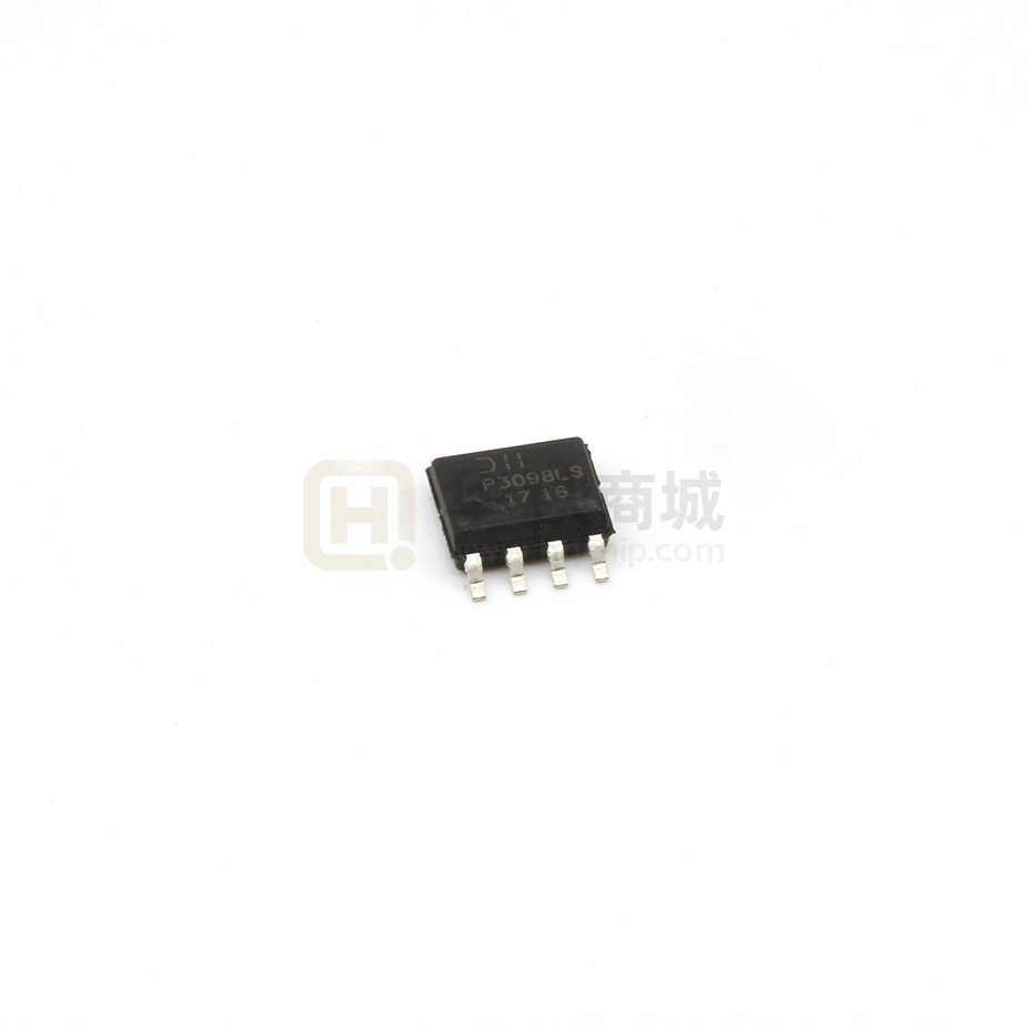
DMP3098LSS
SINGLE P-CHANNEL ENHANCEMENT MODE FIELD EFFECT TRANSISTOR
Please click here to visit our online spice models database.
Features
NEW PRODUCT
•
•
•
•
•
•
•
•
Mechanical Data
•
•
Low On-Resistance
•
65mΩ @ VGS = -10V
•
115mΩ @ VGS = -4.5V
Low Gate Threshold Voltage
Low Input Capacitance
Fast Switching Speed
Low Input/Output Leakage
Lead Free By Design/RoHS Compliant (Note 2)
"Green" Device (Note 4)
Qualified to AEC-Q101 Standards for High Reliability
•
•
•
•
•
•
Case: SOP-8L
Case Material: Molded Plastic, “Green” Molding Compound.
UL Flammability Classification Rating 94V-0
Moisture Sensitivity: Level 1 per J-STD-020D
Terminals Connections: See Diagram
Terminals: Finish - Matte Tin annealed over Copper lead
frame. Solderable per MIL-STD-202, Method 208
Marking Information: See Page 4
Ordering Information: See Page 4
Weight: 0.072g (approximate)
SOP-8L
S
D
S
D
S
D
G
D
TOP VIEW
Internal Schematic
TOP VIEW
Maximum Ratings
@TA = 25°C unless otherwise specified
Characteristic
Units
V
V
IDM
Value
-30
±20
-5.3
-4.7
-20
Characteristic
Total Power Dissipation (Note 1)
Thermal Resistance, Junction to Ambient (Note 1)
Symbol
PD
RθJA
Value
2.5
50
Unit
W
°C/W
Operating and Storage Temperature Range
TJ, TSTG
-55 to +150
°C
Drain-Source Voltage
Gate-Source Voltage
Drain Current (Note 1)
Symbol
VDSS
VGSS
Steady
State
TA = 25°C
TA = 70°C
ID
Pulsed Drain Current (Note 3)
A
A
Thermal Characteristics
Notes:
1.
2.
3.
4.
Device mounted on 2 oz. 1” x 1” Copper pads on 2” x 2” FR-4 PCB.
No purposefully added lead.
Pulse width ≤10μS, Duty Cycle ≤1%.
Diodes Inc.'s "Green" policy can be found on our website at http://www.diodes.com/products/lead_free/index.php.
DMP3098LSS
Document number: DS31265 Rev. 4 - 2
1 of 5
www.diodes.com
September 2008
© Diodes Incorporated
�DMP3098LSS
@TA = 25°C unless otherwise specified
Characteristic
OFF CHARACTERISTICS (Note 5)
Drain-Source Breakdown Voltage
Zero Gate Voltage Drain Current
Gate-Source Leakage
ON CHARACTERISTICS (Note 5)
Gate Threshold Voltage
Symbol
Min
Typ
Max
Unit
BVDSS
IDSS
IGSS
-30
⎯
⎯
⎯
⎯
⎯
⎯
-1
±100
V
μA
nA
VGS = 0V, ID = -250μA
VDS = -30V, VGS = 0V
VGS = ±20V, VDS = 0V
VGS(th)
Test Condition
RDS (ON)
-2.1
65
115
V
Static Drain-Source On-Resistance
⎯
56
98
5.2
⎯
⎯
-1.2
S
V
VDS = VGS, ID = -250μA
VGS = -10V, ID = -5.3A
VGS = -4.5V, ID = -4.2A
VDS = -10V, ID = -5.3A
VGS = 0V, IS = -2A
Forward Transconductance
Diode Forward Voltage (Note 5)
DYNAMIC CHARACTERISTICS
Input Capacitance
Output Capacitance
Reverse Transfer Capacitance
gfs
VSD
-1
⎯
⎯
⎯
-0.5
Ciss
Coss
Crss
⎯
⎯
⎯
336
70
49
⎯
⎯
⎯
pF
pF
pF
VDS = -25V, VGS = 0V
f = 1.0MHz
Gate Resistance
RG
⎯
4.6
⎯
Ω
VDS = 0V, VGS = 0V
f = 1.0MHz
QG
⎯
4.0
⎯
nC
VDS = -15V, VGS = -4.5V,
ID = -5.0A
QG
QGS
QGD
td(on)
tr
td(off)
tf
⎯
⎯
⎯
⎯
⎯
⎯
⎯
7.8
1.0
2.5
6.0
5.0
17.6
9.5
⎯
⎯
⎯
⎯
⎯
⎯
⎯
nC
VDS = -15V, VGS = -10V,
ID = -5.0A
ns
VDS = -15V, VGS = -10V,
ID = -1A, RG = 6.0Ω
mΩ
SWITCHING CHARACTERISTICS
Total Gate Charge
Gate-Source Charge
Gate-Drain Charge
Turn-On Delay Time
Rise Time
Turn-Off Delay Time
Fall Time
Notes:
5. Short duration pulse test used to minimize self-heating effect.
20
20
VDS = -5V
VGS = -10V
12
16
-ID, DRAIN CURRENT (A)
16
-ID, DRAIN CURRENT (A)
NEW PRODUCT
Electrical Characteristics
TA = 25°C
12
VGS = -4.5V
8
4
T A = 150°C
TA = 125°C
TA = -55°C
8
4
VGS = -1.5V
VGS = -2.5V
VGS = -3.0V
0
0
0
1
2
3
4
-VDS, DRAIN-SOURCE VOLTAGE (V)
Fig. 1 Typical Output Characteristics
DMP3098LSS
Document number: DS31265 Rev. 4 - 2
5
1
2
3
4
5
-VGS, GATE SOURCE VOLTAGE (V)
6
Fig. 2 Typical Transfer Characteristics
2 of 5
www.diodes.com
September 2008
© Diodes Incorporated
�DMP3098LSS
1
0.14
RDS(ON), STATIC DRAIN-SOURCE
ON-RESISTANCE (Ω)
0.1
VGS = -10V
0
4
8
12
16
-ID, DRAIN CURRENT (A)
Fig. 3 Typical On-Resistance
vs. Drain Current and Gate Voltage
1.6
RDS(ON), STATIC DRAIN-SOURCE
ON-RESISTANCE (NORMALIZED)
0.12
TA = 125°C
0.10
TA = 85°C
0.08
T A = 25°C
0.06
TA = -55°C
0.04
0.02
0
20
0
2
4
6
8
-ID, DRAIN CURRENT (A)
Fig. 4 Typical On-Resistance
vs. Drain Current and Temperature
10
1,000
1.4
VGS = -10V
ID = -5.3A
VGS = -4.5V
ID = -4.2A
1.2
1.0
C, CAPACITANCE (pF)
RDS(ON), STATIC DRAIN-SOURCE
ON-RESISTANCE (Ω)
VGS = -4.5V
0.01
Ciss
100
Coss
Crss
0.8
0.6
-50
10
-25
0
25
50
75 100 125 150
TA, AMBIENT TEMPERATURE (°C)
Fig. 5 On-Resistance Variation with Temperature
0
-IS, SOURCE CURRENT (A)
2.0
ID = -250µA
1.6
1.2
0.8
-50
Document number: DS31265 Rev. 4 - 2
30
8
TA = 25°C
6
4
2
0
-25
0
25
50
75 100 125 150
TA, AMBIENT TEMPERATURE (°C)
Fig. 7 Gate Threshold Variation vs. Ambient Temperature
DMP3098LSS
5
10
15
20
25
-VDS, DRAIN-SOURCE VOLTAGE (V)
Fig. 6 Typical Capacitance
10
2.4
-VGS(TH), GATE THRESHOLD VOLTAGE (V)
NEW PRODUCT
TA = 150°C
3 of 5
www.diodes.com
0.4
0.6
0.8
1
-VSD, SOURCE-DRAIN VOLTAGE (V)
Fig. 8 Diode Forward Voltage vs. Current
1.2
September 2008
© Diodes Incorporated
�DMP3098LSS
1
NEW PRODUCT
r(t), TRANSIENT THERMAL RESISTANCE
D = 0.7
D = 0.5
D = 0.3
0.1
D = 0.1
D = 0.9
D = 0.05
RθJA(t) = r(t) * RθJA
RθJA = 101°C/W
D = 0.02
0.01
P(pk)
D = 0.01
t2
T J - T A = P * R θJA(t)
Duty Cycle, D = t1 /t2
D = 0.005
D = Single Pulse
0.001
0.00001
t1
0.0001
0.001
0.01
0.1
1
t1, PULSE DURATION TIME (s)
10
100
1,000
Fig. 9 Transient Thermal Response
Ordering Information
(Note 6)
Part Number
DMP3098LSS-13
Notes:
Case
SOP-8L
Packaging
2500/Tape & Reel
6. For packaging details, go to our website at http://www.diodes.com/datasheets/ap02007.pdf.
Marking Information
Top View
8
5
Logo
P3098LS
Part no.
YY WW
1
4
Xth week: 01~52
Year : "07" =2007
"08" =2008
0.254
Package Outline Dimensions
E1 E
A1
L
Gauge Plane
Seating Plane
Detail ‘A’
7°~9°
h
45°
A2 A A3
Detail ‘A’
b
e
D
DMP3098LSS
Document number: DS31265 Rev. 4 - 2
4 of 5
www.diodes.com
SOP-8L
Dim
Min
Max
A
1.75
A1
0.08
0.25
A2
1.40
1.50
A3
0.20 Typ
b
0.3
0.5
D
4.85
4.95
E
5.90
6.10
E1
3.80
3.90
e
1.27 Typ
h
0.35
L
0.60
0.80
0°
8°
θ
All Dimensions in mm
September 2008
© Diodes Incorporated
�DMP3098LSS
Suggested Pad Layout
NEW PRODUCT
X
C1
Dimensions
X
Y
C1
C2
Value (in mm)
0.60
1.55
5.4
1.27
C2
Y
IMPORTANT NOTICE
Diodes Incorporated and its subsidiaries reserve the right to make modifications, enhancements, improvements, corrections or other changes
without further notice to any product herein. Diodes Incorporated does not assume any liability arising out of the application or use of any product
described herein; neither does it convey any license under its patent rights, nor the rights of others. The user of products in such applications shall
assume all risks of such use and will agree to hold Diodes Incorporated and all the companies whose products are represented on our website,
harmless against all damages.
LIFE SUPPORT
Diodes Incorporated products are not authorized for use as critical components in life support devices or systems without the expressed written
approval of the President of Diodes Incorporated.
DMP3098LSS
Document number: DS31265 Rev. 4 - 2
5 of 5
www.diodes.com
September 2008
© Diodes Incorporated
�


 工商网监
湘ICP备2023018690号
工商网监
湘ICP备2023018690号
