User's Guide
SLVU536A – June 2012 – Revised October 2012
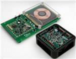
bq500211 bqTESLA Wireless Power TX EVM
The bqTESLA™ wireless power transmitter evaluation module from Texas Instruments is a highperformance, easy-to-use development module for the design of wireless power solutions. The singlechannel transmitter enables designers to speed the development of their end-applications. The
bq500211EVM evaluation module (EVM) provides all basic functions of a Qi-compliant, wireless charger
pad. The EVM is intended to be used with bq51013AEVM-764, -765 or any other Qi-compliant receiver.
The transmitter EVM is a 5-V input design which powers a standard WPC low-power 5-W receiver. The
bq500211EVM-045 will support bq500211 device.
1
2
3
4
5
6
7
8
Contents
Applications .................................................................................................................. 2
bq500211EVM-045 Electrical Performance Specifications ............................................................ 2
Modifications ................................................................................................................. 2
Connector and Test Point Descriptions .................................................................................. 3
4.1
Input/Output Connections ......................................................................................... 3
4.2
Test Point Descriptions ............................................................................................ 3
Schematic and Bill of Materials ........................................................................................... 5
Test Setup .................................................................................................................. 10
6.1
Equipment ......................................................................................................... 10
6.2
Equipment Setup ................................................................................................. 10
bq500211EVM-045 Assembly Drawings and Layout ................................................................. 12
Reference ................................................................................................................... 16
List of Figures
1
bq500211EVM-045 Schematic, Page 1 of 3 ............................................................................ 5
2
bq500211EVM-045 Schematic, Page 2 of 3 ............................................................................ 6
3
bq500211EVM-045 Schematic, Page 3 of 3 ............................................................................ 7
4
Equipment Setup .......................................................................................................... 11
5
Efficiency versus Power, bq500211EVM-045 Transmitter and HPA764 Receiver
6
7
8
9
10
11
...............................
Assembly Top ..............................................................................................................
Top Silk .....................................................................................................................
Top Layer ...................................................................................................................
Layer 2 ......................................................................................................................
Layer 3 ......................................................................................................................
Bottom Layer ...............................................................................................................
12
13
13
14
14
15
15
List of Tables
1
bq500211EVM-045 Electrical Performance Specifications ............................................................ 2
2
Bill of Materials .............................................................................................................. 8
bqTESLA is a trademark of Texas Instruments.
SLVU536A – June 2012 – Revised October 2012
Submit Documentation Feedback
bq500211 bqTESLA Wireless Power TX EVM
Copyright © 2012, Texas Instruments Incorporated
1
�Applications
1
www.ti.com
Applications
The bq500211EVM-045 evaluation module demonstrates the transmitter portion of the bqTESLA™
wireless power system. This transmitter EVM is a complete transmitter-side solution that powers a
bqTESLA™ receiver. The bq500211EVM requires a single 5-V power supply capable of up to 2 A to
operate and combines the transmitter electronics, input power socket, LED indicators, and the transmitting
coil on the single printed-circuit board (PCB). The open design allows easy access to key points of the
electrical schematic. The board has an installed serial interface connector for more advanced operation.
This EVM has the following features.
• Dynamic Power Limiting™ (DPL) allows operation from a 5-V supply with limited current capability (for
example, a USB port).
• Transmitter-coil mounting pad providing the correct receiver interface
• Input power is really available 5 V
• Standard WPC A5-type transmitter coil
• LED indicates power transfer or power fault state
• Audio indication of start-of-power transfer though a board-mounted buzzer
2
bq500211EVM-045 Electrical Performance Specifications
Table 1 provides a summary of the bq500211EVM-045 performance specifications. All specifications are
given for an ambient temperature of 25°C.
Table 1. bq500211EVM-045 Electrical Performance Specifications
Parameter
Notes and Conditions
Min
Typ
Max
Unit
Input Characteristics
VIN
Input voltage
5.0
5.10
V
IIN
Input current
VIN = Nom, IOUT = Max
4.90
1.50
2.0
A
Input no-load current
VIN = Nom, IOUT = 0 A
200
mA
Input stand-by current
VIN = Nom
20
mA
Output Characteristics – Receiver bq51013AEVM-764 or 765
VOUT
IOUT
Output voltage
VIN = Nom, IOUT = Nom
Output ripple
VIN = Nom, IOUT = Max
4.5
5
5.1
V
200
mVPP
VIN = Min to Max
VIN = Min to Max
0
1
A
Output overcurrent
VIN = Nom
1
1.1
A
205
kHz
Systems Characteristics
3
FS
Switching frequency
Switching frequency varies with load
ηpk
Peak efficiency
VIN = Nom, P Out RX = 2.5 W
110
72
%
η
Full-load efficiency
VIN = Nom, IOUT = Max
70
%
Modifications
See the data sheet (SLUSAO2) when changing components. The board is laid out so that a shield can be
placed over the active circuit area; Laird Technology BMIS-207 can be used.
Use LED Mode – Resistor R23 to change the behavior of the status LED, D4. The standard value is
42.2 kΩ for control option 1, see the data sheet for additional settings.
NTC – Connector JP1 provides the option for connecting a negative temperature coefficient (NTC)
sensor for thermal protection, see the data sheet for additional settings.
EMI Shield – The board is laid out so that a shield can be placed over the active circuit area, Laird
Technology BMIS-207 can be used
2
bq500211 bqTESLA Wireless Power TX EVM
Copyright © 2012, Texas Instruments Incorporated
SLVU536A – June 2012 – Revised October 2012
Submit Documentation Feedback
�Connector and Test Point Descriptions
www.ti.com
4
Connector and Test Point Descriptions
4.1
Input/Output Connections
The connection points are described in the following paragraphs.
4.1.1
J1 – VIN
Input power 5 V ±100 mV, return at J2.
4.1.2
J2 – GND
Return for input power, input at J1.
4.1.3
J3 –JTAG
Factory use only
4.1.4
J4 – Serial Interface
Factory use only
4.1.5
JP2 – LED Mode
External connection for LED MODE reistor, if R23 is removed.
4.1.6
JP4 – Select for Normal or Power Limiting
Shorting this header enables the Dynamic Power Limiting feature and the input current is limited to 500
mA. With this connector open, operation is normal, there is no restriction on input power.
4.1.7
JP3 – PMOD Enable (Future Use)
Not used for the bq500211 device, should be open.
4.1.8
JP1 – NTC
The connection point for the external temperature sensor. See the data sheet for more information.
4.2
Test Point Descriptions
The test points are described in the following paragraphs.
4.2.1
TP1 – Coil Drive Q1 / Q2
H-Bridge drive signal.
4.2.2
TP2 – Coil Monitor L / C
Coil signal at junction between coil and capacitors.
4.2.3
TP3 – PWR GND
Ground for switch circuits.
4.2.4
TP4 – Analog GND
Low-noise GND
SLVU536A – June 2012 – Revised October 2012
Submit Documentation Feedback
bq500211 bqTESLA Wireless Power TX EVM
Copyright © 2012, Texas Instruments Incorporated
3
�Connector and Test Point Descriptions
4.2.5
www.ti.com
TP5 – Analog GND
Low-noise GND
4.2.6
TP6 – Analog GND
Low-noise GND
4.2.7
TP7 – Analog GND
Low-noise GND
4.2.8
TP8 – DC Buzzer Output
The connection point for an external DC buzzer; logic high for 500 ms at the start of power transfer to
receiver unit.
4.2.9
TP9 – 3.3-VDC
Voltage for low-power circuits, 3.3-V output from U5, TPS62237, U5.
4.2.10
TP10 - Filtered 3.3 V
3.3-V output with additional filtering for A-to-D converters.
4.2.11
TP11 – Input voltage
Input voltage from J1.
4.2.12
TP12 – MSP430 3.3 V
Filtered 3.3 V for MSP430, U4.
4.2.13
TP13 – Demodulation Comm 1 Output
Primary communications channel, input to bq500211, U1 from demodulation circuit.
4.2.14
TP14 – Sleep
Output from bq500211, U1 to sleep timer circuit.
4.2.15
TP15 – Coil Drive Q3 and Q4 Side
H-Bridge drive signal Q3 and Q4.
4.2.16
TP16 – DPWM Signal
Digital output signal from bq500211 to H-Bridge drive for Q1 and Q2.
4.2.17
TP17 – DPWM Signal
Digital output signal from bq500211 to H-Bridge drive for Q3 and Q4.
4.2.18
TP18 – Spare Pin
Unused output from bq500211.
4.2.19
TP19 – I_Sense
Input current-sense voltage, scale 1 V = 1 A.
4
bq500211 bqTESLA Wireless Power TX EVM
Copyright © 2012, Texas Instruments Incorporated
SLVU536A – June 2012 – Revised October 2012
Submit Documentation Feedback
�Schematic and Bill of Materials
www.ti.com
5
Schematic and Bill of Materials
Buck Regulator
VIN
J1
TP11
1
D C IN
5 Vin
2
C26
4.7uF
R4
D3
C2
1
4.7uF
TP9
1
SW 2
FB 6
3 VIN
5 EN
1 M ODE
365
L1
1.0 uH
U5
TPS62237D RY
GND 4
2
3V3_VCC
C25
4.7uF
J5
D C IN
1
GND
2
D1
R25
1
Pow er Train
523k
LTST-C190G KT
TP4 TP5 TP6 TP7
VIN
GND
2
J2
R37
200
U7
LM V931ID CK
VIN
TP14
SLEEP
Q4
BSS138
R36
200
.020 O hm
C22
4.7uF
Q6
BC857C
R32
C7
22uF
C21
TP19
I_SEN SE
0.1uF
C16
0.01uF
R46
10.0k
R18
10.0k
U2
TPS28225D
VIN
D PW M -1A
6 VD D
3 PW M
U G ATE 1
BO O T 2
7 EN /PG
4 GND
PH SE 8
LG ATE 5
Q1
CSD 17308Q 3
Q3
CSD 17308Q 3
C23
22uF
R3
10.0
TP1
L2
IN D _TXL05001 TP2
TP15
C6 0.22uF
C27
Q2
CSD 17308Q 3
C9
0.1uF
R34
0
C18
4700pF
C15
0.22uF
100nF
C28 100nF
C29
100nF
3V3_VCC C30
100nF
Q5
R6
100k
TP13
R29
10
R14
23.2k
U6
TPS28225D
1 U G ATE
VD D 6
2 BO O T
PW M 3
8 PH SE
5 LG ATE
VIN
EN /PG 7
GND 4
C13
0.1uF
CSD 17308Q 3
TP3
R1
10.0
R13
0
D2
CO M M +
BAT54SW
R26
10
R5
10.0k
C14
33pF
CO M M -
Figure 1. bq500211EVM-045 Schematic, Page 1 of 3
SLVU536A – June 2012 – Revised October 2012
Submit Documentation Feedback
bq500211 bqTESLA Wireless Power TX EVM
Copyright © 2012, Texas Instruments Incorporated
5
�Schematic and Bill of Materials
www.ti.com
U3
TLV70033D CK
VIN
1 IN
2 GND
C17
0.1uF
Low Pow er Supervisor
R24
10
O UT 5
3V3_VCC
3 EN
NC 4
-
C11
4.7uF
R16
C8
1.0uF
C10
0.01uF
R12
10.0k
Q7
BSS138
10.0k
M SP_RST
U4
M SP430G 2001
TP12
Tem p Sensor
TP10
3V3_AD C
3V3_VCC
R19
10.0k
R7
22
JP1
C24
4.7nF
M SP_CLK
M SP_M ISO
C19
4.7uF
C1 1.0uF
3V3_VCC
R10
15.4k
VIN
2.00k
I_SEN SE
4700pF
SLEEP
M SP_RST
M SP_M ISO
M SP_TEST
TP18
M SP_CLK
3V3_VCC
CO M M +
CO M M -
1.0uF
M SP_SYN C
3 P1.1
4 P1.2
XO U T 12
TEST 11
M SP_TEST
5 P1.3
6 P1.4
RST 10
P1.7 9
C12
1000pF
7 P1.5
P1.6 8
M SP_M O SI
M SP_RD Y
R33
10.0k
R15
V33D 33
41 V33FB
48 REFIN
BPCAP35
JTAG _TRSTN31
JTAG _TM S30
JTAG _TD I29
5 RESET
U1
JTAG _TD O28
BQ 500211RG ZJTAG _TCK27
4 AIN 8
PM B_CTRL20
3 AIN 3
PM B_ALRT19
2 T_SEN SE
AIN
5
PM
B_D ATA11
1
PM B_CLK10
46 V_IN
45 AIN 7
D PW M _A12
42 I_IN
D PM B_B13
M SP_SYN C14
D
O U T_2B15
SLEEP
6
D O U T_4A16
7 M SP_RST/LED _A
D O U T_4B17
8 M SP_M ISO /LED _B
9 M SP_TEST
18 M SP_TCK/CLK M SP_TD O /PRO G26
21 D O U T_TX M SP_M O SI/LPW R_EN
25
22 D RV_CFG
BU Z_D C24
BU Z_AC23
37 CO M M _A+
R45
38 CO M M _A10.0k
39 CO M M _B+
LED _M O D E44
40 CO M M _BPM O D _TH R43
BQ 500211
1
C3
47 AG N D
36 AG N D
32 D G N D
49 EPAD
10K
R9
JP4
R11
4.7uF
10.0k
R30
G N D 14
XIN 13
AG N D
100k
R20
C4
C5
V33A34
3V3_VCC
1 VCC
2 P1.0
R28
470
1.0uF C20
R27
470
1
R8
10.0k
/TRST
TM S
TD I
TD O
TCK
STATU S
PM _D ATA
PM _CLK
R47
10.0
D4
H SM F-C165
R2
10.0
TP17
TP16
D PW M -1A
M SP_SYN C
D PW M -1B
R48
10.0k
M SP_RD Y
M SP_M O SI
TP8
R17
10.0k
AG N D
BU Z
R44
475
R22
JP3
R23
42.2k
JP2
D5
LTST-C190G KT
Parts w ith no values are not installed
Figure 2. bq500211EVM-045 Schematic, Page 2 of 3
6
bq500211 bqTESLA Wireless Power TX EVM
SLVU536A – June 2012 – Revised October 2012
Submit Documentation Feedback
Copyright © 2012, Texas Instruments Incorporated
�Schematic and Bill of Materials
www.ti.com
J4
14
13
12
11
10
9
8
7
6
5
4
3
2
1
TCK
TD O
TD I
/TRST
TM S
1
2
3
4
5
6
7
8
9
10
PM _CLK
PM _D ATA
J3
R40
R41
10.0k 10.0k
3V3_VCC
R43
10.0k
R21
R31
R35 R38
R49
R39
R42
3V3_VCC
SH D 1
Figure 3. bq500211EVM-045 Schematic, Page 3 of 3
SLVU536A – June 2012 – Revised October 2012
Submit Documentation Feedback
bq500211 bqTESLA Wireless Power TX EVM
Copyright © 2012, Texas Instruments Incorporated
7
�Schematic and Bill of Materials
www.ti.com
Table 2. Bill of Materials
Count
RefDes
Value
Description
Size
Part Number
MFR
1
BUZ
Buzzer
Piezoelectronic, 12 mm
12 mm
PS1240P02CT3
TDK
1
C14
33pF
Capacitor, Ceramic, 50V, C0G, 5%
0603
Std
Std
1
C12
1000pF
Capacitor, Ceramic, 10V, COG, 5%
0603
Std
Std
2
C4, C18, C24
4700pF
Capacitor, Ceramic, 50V, X7R, 10%
0603
Std
Std
2
C16, C10
0.01uF
Capacitor, Ceramic, 50V, X7R, 10%
0603
Std
Std
4
C13, C21, C17, C9
0.1uF
Capacitor, Ceramic, 50V, X7R, 10%
0603
Std
Std
4
C27, C28, C29, C30
100nF
Capacitor, Ceramic, COG, 50V, 5%
1812
C4532COG1H104J
TDK
2
C15, C6
0.22uF
Capacitor, Ceramic, 50V, X7R, 20%
0603
Std
Std
4
C1, C3, C8, C20
1.0uF
Capacitor, Ceramic, 16V, X7R, 20%
0603
Std
Std
7
C22, C25, C5, C11, C19, C26, 4.7uF
C2
Capacitor, Ceramic, 10V, X5R, 20%
0603
Std
Std
2
C23, C7
22uF
Capacitor, Ceramic, 25V, X5R, 20%
1210
Std
Std
2
D1, D5
LTST-C190GKT
Diode, LED, Green, 2.1-V, 20-mA, 6-mcd
0603
LTST-C190GKT
Lite On
1
D2
BAT54SW
Diode, Dual Schottky, 200mA, 30V
SOT523
BAT54SWT1G
On Semi
0
D3
Open
Diode, Schottky, 0.5A, 30V
SOD-123
MMSZ5251BT1G
On Semi
1
D4
HSMF-C165
Diode, Bi-Color LED, [GRN/RED] 20mA, 52 mW Max.
0603
HSMF-C165
Avago
1
L1
1.0 uH
Inductor, SMT, 800 mA, ±20%
0805
LQM21PN1R0MC0
Murata
Alternate L1
1.0 uH
Inductor, SMT, 800 mA, ±20%
0805
74479775210
Wurth
L2
6.3 uH
Inductor, WPC TX Coil
53 × 53 mm
TXL05001A (or B)
Mingstar
1
Alternate L2
6.3 uH
Inductor, WPC TX Coil
52 X 53 mm
760-308-105
Wurth
4
Q1, Q2, Q3, Q5
CSD17308Q3
MOSFET, NChan, 30V, 13A, 9.4 milliOhm
QFN3.3x3.3 mm
CSD17308Q3
TI
2
Q4, Q7
BSS138
MOSFET, Nch, 50V, 0.22A, 3.5 Ohm
SOT23
BSS138
Fairchild
1
Q6
BC857C
Trans, P-Chan GP, 65V, 100mA,
SOT-23
BC857
Philips
1
R10
15.4k
Resistor, Chip, 1/16W, 1%
0603
Std
Std
1
R11
2.00k
Resistor, Chip, 1/16W, 1%
0603
Std
Std
2
R13, R34
0
Resistor, Chip, 1/16W, 1%
0603
Std
Std
1
R32
0.020 Ohm
Resistor, Chip, 1/4W, 1%, 200ppm
0805
ERJ-6BWFR020V
Panasonic
6
R1-3, R24, R26, R29
10
Resistor, Chip, 1/16W, 1%
0603
Std
Std
1
R7
22
Resistor, Chip, 1/10W, 1%
0805
Std
Std
2
R36, R37
200
Resistor, Chip, 1/16W, 1%
0603
Std
Std
1
R4
365
Resistor, Chip, 1/16W, 1%
0603
Std
Std
2
R27, R28
470
Resistor, Chip, 1/16W, 1%
0603
Std
Std
1
R38
475
Resistor, Chip, 1/16W, 1%
0603
Std
Std
8
bq500211 bqTESLA Wireless Power TX EVM
SLVU536A – June 2012 – Revised October 2012
Submit Documentation Feedback
Copyright © 2012, Texas Instruments Incorporated
�Schematic and Bill of Materials
www.ti.com
Table 2. Bill of Materials (continued)
Count
RefDes
Value
Description
Size
Part Number
MFR
15
R5, R8, R9, R12, R16-19,
R30, R31, R33, R35, R39,
R40, R43
10.0k
Resistor, Chip, 1/16W, 1%
0603
Std
Std
1
R14
23.2k
Resistor, Chip, 1/16W, 1%
0603
Std
Std
1
R23
42.2k
Resistor, Chip, 1/16W, 1%
0603
Std
Std
2
R6, R20
100k
Resistor, Chip, 1/16W, 1%
0603
Std
Std
1
R20
100k
Resistor, Chip, 1/16W, 1%
0402
Std
Std
1
R25
523k
Resistor, Chip, 1/16W, 1%
0603
Std
Std
0
R15, R22, R21, R31, R35,
R49, R39, R42
Open
Resistor, Chip, 1/16W, 1%
0603
Std
Std
1
U1
BQ500211RGZ
IC, Qi Compliant Wireless Power Transmitter Manager
7X7 QFN
BQ500211RGZ (R/T)
TI
2
U2 U6
TPS28225D
IC, High Frequency 4-Amp Sink Synchronous Buck MOSFET SO8
Driver
TPS28225D
TI
1
U4
MSP430G2001
IC, Mixed Signal Microcontroller
TSSOP
MSP430G2001IPW14
TI
1
U5
TPS62237DRY
IC, 3MHz Ultra Small Step Down Converter, 3.3 V
USON
TPS62237DRY
TI
1
U7
LMV931IDCK
IC, Single Op-Amp R-R In/Out put
SC-70
LMV931IDCK
TI
1
U8
TLV70033DCK
IC, 150mA, Low IQ, LDO Regulator
SOT
TLV70033DCK
TI
0
SHD1
Open
Shield, Copper
44.4x44.4 mm
BMI-S-207-F
Laird Tech
SLVU536A – June 2012 – Revised October 2012
Submit Documentation Feedback
bq500211 bqTESLA Wireless Power TX EVM
Copyright © 2012, Texas Instruments Incorporated
9
�Test Setup
www.ti.com
6
Test Setup
6.1
Equipment
6.1.1
bqTESLA™ Receiver
Use the bq51013AEVM-764 or a Qi-compliant receiver to work with this EVM.
6.1.2
Voltage Source
The input voltage source must provide a regulated DC voltage of 5 V and deliver at least 2-A continuous
load current; current limit must be set to 3 A.
CAUTION
To help assure safety integrity of the system and minimize risk of electrical
shock hazard, always use a power supply providing suitable isolation and
supplemental insulation (double insulated). Compliance to IEC 61010-1,
Safety Requirements for Electrical Equipment for Measurement, Control and
Laboratory Use, Part 1, General Requirements, or its equivalent is strongly
suggested, including any required regional regulatory compliance
certification approvals. Always select a power source that is suitably rated
for use with this EVM as referenced in this user manual.
6.1.3
Meters
Monitor the output voltage at the bq51013AEVM-764 test point TP7 with a voltmeter. Monitor the input
current into the load with an appropriate ammeter. You can also monitor the transmitter input current and
voltage, but the meter must use the averaging function for reducing error, due to communications packets.
6.1.4
Loads
A single load is required at 5 V with a maximum current of 1 A. The load can be resistive or electronic.
6.1.5
Oscilloscope
Use a dual-channel oscilloscope with appropriate probes to observe the COMM_DRV signal at
bq51013AEVM-764 TP3 and other signals.
6.1.6
Recommended Wire Gauge
For proper operation, use 22-AWG wire when connecting the bq500211EVM-045 to the input supply and
the bq51013AEVM-764 to the load.
6.2
Equipment Setup
•
•
•
6.2.1
With the power supply OFF, connect the supply to the bqTESLA™ transmitter.
Connect the VIN positive power source to J1, and connect the negative terminal of the VIN source to J2.
Do not place the bqTESLA™ receiver on the transmitter. Connect a load to J3 with a return to J4,
monitor current through the load with the ammeter, and monitor the current to the load at TP7. All
voltmeters must be Kelvin connected (at the pin) to the point of interest.
Equipment Setup Diagram
The diagram in Figure 4 shows the test setup.
10
bq500211 bqTESLA Wireless Power TX EVM
Copyright © 2012, Texas Instruments Incorporated
SLVU536A – June 2012 – Revised October 2012
Submit Documentation Feedback
�Test Setup
www.ti.com
Wireless Transmitter
bq500211EVM-045
Wireless Receiver
bq51013EVM-725
A
OUT_J2
J1
POS
A
VIN
+
-
TP1
AC1
LP
V
J2
RTN
V
AC1
Voltmeter
TP2
AC2
OUT_TP7
VRECT_TP12
LS
V
RL
AC2
GND_J4
A
Ammeter
+
-
Power Supply
Oscilloscope
Figure 4. Equipment Setup
6.2.2
EVM Procedures
This section guides the user through a few general test procedures to exercise the functionality of the
presented hardware. Some key notes follow.
6.2.2.1
Start-Up No Receiver
Turn on VIN, and observe that the green power LED, D1, illuminates. Status LED D5 is off until the power
transfer starts.
Apply the scope probe to the test point, TP1, and observe single-pulse bursts approximately every 400
ms. This is an analog ping probing environment for the presence of a receiver placed on the TX coil.
6.2.2.2
Apply Receivers
Place the bq51013AEVM-764 EVM on the top of the transmitting coil. Align the centers of the receiving
and transmitting coils across each other. In the next few seconds, observe that the status LED, D5,
flashes green, indicating that communication between the transmitter and the receiver is established and
that power transfer has started.
• The buzzer sounds at the start of power transfer. The status LED, D4, flashes a green light during
power transfer.
• Typical output voltage is 5 V, and the output current range is 0 mA to 1 A.
• Observe a continuous sine-wave on the test point TP1 when power transfer is active; the frequency is
between 110 kHz and 205 kHz.
• Make tests and measurements applicable to a normal 5-V power supply.
6.2.2.3
Efficiency
To measure system efficiency, measure the output voltage, the output current, input voltage, and input
current and calculate efficiency as the ratio of the output power to the input power. Connect voltage
meters at the input and output of TX and RX (see Figure 4). Average the input current; the comm pulses
modulate the input current, distorting the reading. See Figure 5 for efficiency.
SLVU536A – June 2012 – Revised October 2012
Submit Documentation Feedback
bq500211 bqTESLA Wireless Power TX EVM
Copyright © 2012, Texas Instruments Incorporated
11
�bq500211EVM-045 Assembly Drawings and Layout
www.ti.com
80
70
Efficiency (%)
60
50
40
30
20
10
0
0.0
0.5
1.0
1.5
2.0
2.5
3.0
3.5
4.0
Power (W)
4.5
5.0
C001
Figure 5. Efficiency versus Power, bq500211EVM-045 Transmitter and HPA764 Receiver
6.2.2.4
Dynamic Power Limiting™
Dynamic Power Limiting™ (DPL) allows operation from a 5-V supply with limited current capability. DPL is
controlled by JP4, which pulls U1 pin 4 high or low. With the jumper open (pin 4 High) the IC monitors
input voltage and when that voltage is observed drooping, the output power is limited to reduce the load
and provide some operating margin relative to the supply’s capability. With a shorting jumper installed
(pin 4 Low), the IC restricts output power such that the input current remains below 500 mA, compatible
with a USB port. See the data sheet for additional information on the DPL function
6.2.2.5
Thermal Protection, NTC
Thermal protection is provided by an NTC resistor connected to JP1. At 1 V on the sense side (U1-2), the
thermal fault is set, and the unit is shut down, The status LED, D5, illuminates red. The typical resistor
value for fault is 850 Ω. The system tries to restart in 5 minutes.
7
bq500211EVM-045 Assembly Drawings and Layout
Figure 6 through Figure 11 show the design of the bq500211EVM PCB. The EVM has been designed
using a 4-layer, 2-oz, copper-clad circuit board 13.2 cm × 7.24 cm with all components in a 4.5-cm x 4.5cm active area on the top side and all active traces to the top and bottom layers to allow the user to easily
view, probe, and evaluate the bq500211 control IC in a practical application. Moving components to both
sides of the PCB or using additional internal layers offers additional size reduction for space-constrained
systems. Gerber files are available for download from the EVM product folder.
A 4-layer PCB design is recommended to provide a good low-noise ground plane for all circuits. A 2-layer
PCB presents a high risk of poor performance. Grounding between the bq500211 GND pin 47, 36 and 32
and filter capacitor returns C19, C1, C5 and C3 should be a good low-impedance path.
Coil Grounding – A ground plane area under the coil is recommended to reduce noise coupling into the
receiver. The ground plane for the EVM is slightly larger than the coil footprint and grounded at one point
back to the circuit area.
Note: The clear plastic cover thickness is 0.93 in, or 2.4 mm is the z-gap thickness for the transmitter.
12
bq500211 bqTESLA Wireless Power TX EVM
Copyright © 2012, Texas Instruments Incorporated
SLVU536A – June 2012 – Revised October 2012
Submit Documentation Feedback
�bq500211EVM-045 Assembly Drawings and Layout
www.ti.com
Figure 6. Assembly Top
Figure 7. Top Silk
SLVU536A – June 2012 – Revised October 2012
Submit Documentation Feedback
bq500211 bqTESLA Wireless Power TX EVM
Copyright © 2012, Texas Instruments Incorporated
13
�bq500211EVM-045 Assembly Drawings and Layout
www.ti.com
Figure 8. Top Layer
Figure 9. Layer 2
14
bq500211 bqTESLA Wireless Power TX EVM
Copyright © 2012, Texas Instruments Incorporated
SLVU536A – June 2012 – Revised October 2012
Submit Documentation Feedback
�bq500211EVM-045 Assembly Drawings and Layout
www.ti.com
Figure 10. Layer 3
Figure 11. Bottom Layer
SLVU536A – June 2012 – Revised October 2012
Submit Documentation Feedback
bq500211 bqTESLA Wireless Power TX EVM
Copyright © 2012, Texas Instruments Incorporated
15
�Reference
8
www.ti.com
Reference
For additional information about the bq500211EVM-045 low-power, wireless, power evaluation kit from
Texas Instruments, visit the product folder on the TI Web site at
http://focus.ti.com/docs/toolsw/folders/print/bq500211.html.
16
bq500211 bqTESLA Wireless Power TX EVM
Copyright © 2012, Texas Instruments Incorporated
SLVU536A – June 2012 – Revised October 2012
Submit Documentation Feedback
�EVALUATION BOARD/KIT/MODULE (EVM) ADDITIONAL TERMS
Texas Instruments (TI) provides the enclosed Evaluation Board/Kit/Module (EVM) under the following conditions:
The user assumes all responsibility and liability for proper and safe handling of the goods. Further, the user indemnifies TI from all claims
arising from the handling or use of the goods.
Should this evaluation board/kit not meet the specifications indicated in the User’s Guide, the board/kit may be returned within 30 days from
the date of delivery for a full refund. THE FOREGOING LIMITED WARRANTY IS THE EXCLUSIVE WARRANTY MADE BY SELLER TO
BUYER AND IS IN LIEU OF ALL OTHER WARRANTIES, EXPRESSED, IMPLIED, OR STATUTORY, INCLUDING ANY WARRANTY OF
MERCHANTABILITY OR FITNESS FOR ANY PARTICULAR PURPOSE. EXCEPT TO THE EXTENT OF THE INDEMNITY SET FORTH
ABOVE, NEITHER PARTY SHALL BE LIABLE TO THE OTHER FOR ANY INDIRECT, SPECIAL, INCIDENTAL, OR CONSEQUENTIAL
DAMAGES.
Please read the User's Guide and, specifically, the Warnings and Restrictions notice in the User's Guide prior to handling the product. This
notice contains important safety information about temperatures and voltages. For additional information on TI's environmental and/or safety
programs, please visit www.ti.com/esh or contact TI.
No license is granted under any patent right or other intellectual property right of TI covering or relating to any machine, process, or
combination in which such TI products or services might be or are used. TI currently deals with a variety of customers for products, and
therefore our arrangement with the user is not exclusive. TI assumes no liability for applications assistance, customer product design,
software performance, or infringement of patents or services described herein.
REGULATORY COMPLIANCE INFORMATION
As noted in the EVM User’s Guide and/or EVM itself, this EVM is subject to the Federal Communications Commission (FCC), Industry
Canada (IC) and European Union CE Mark rules.
FCC – FEDERAL COMMUNICATIONS COMMISSION Part 18 Compliant
Note: This equipment has been tested and found to comply with the limits for a Class B digital device, pursuant to part 18 of the FCC
Rules. These limits are designed to provide reasonable protection against harmful interference in a residential installation. This equipment
generates, uses and can radiate radio frequency energy and, if not installed and used in accordance with the instructions, may cause
harmful interference to radio communications. However, there is no guarantee that interference will not occur in a particular installation. If
this equipment does cause harmful interference to radio or television reception, which can be determined by turning the equipment off and
on, the user is encouraged to try to correct the interference by one or more of the following measures:—Reorient or relocate the receiving
antenna.
• Increase the separation between the equipment and receiver.
• Connect the equipment into an outlet on a circuit different from that to which the receiver is connected.
• Consult the dealer or an experienced radio/TV technician for help.
Note: There is no required maintenance of this device from a FCC compliance perspective.
IC – INDUSTRY CANADA ICES-001 Compliant
This ISM device complies with Canadian ICES-001.
Cet appareil ISM est conforme à la norme NMB-001 du Canada.
European Union CE Mark
This ISM device complies with Directive 2004/108/EC of the European Parliament and of the Council of 15 December 2004 on the
approximation of the laws of the Member States relating to electromagnetic compatibility and repealing Directive 89/336/EEC – the EMC
Directive, tested to EN55011: 2007, Industrial Scientific and Medical (ISM) radio-frequency equipment.
SPACER
SPACER
SPACER
SPACER
SPACER
SPACER
SPACER
SPACER
SPACER
�EVALUATION BOARD/KIT/MODULE (EVM)
WARNINGS, RESTRICTIONS AND DISCLAIMERS
For Feasibility Evaluation Only, in Laboratory/Development Environments. Unless otherwise indicated, this EVM is not a finished
electrical equipment and not intended for consumer use. It is intended solely for use for preliminary feasibility evaluation in
laboratory/development environments by technically qualified electronics experts who are familiar with the dangers and application risks
associated with handling electrical mechanical components, systems and subsystems. It should not be used as all or part of a finished end
product.
Your Sole Responsibility and Risk. You acknowledge, represent and agree that:
1.
2.
3.
4.
You have unique knowledge concerning Federal, State and local regulatory requirements (including but not limited to Food and Drug
Administration regulations, if applicable) which relate to your products and which relate to your use (and/or that of your employees,
affiliates, contractors or designees) of the EVM for evaluation, testing and other purposes.
You have full and exclusive responsibility to assure the safety and compliance of your products with all such laws and other applicable
regulatory requirements, and also to assure the safety of any activities to be conducted by you and/or your employees, affiliates,
contractors or designees, using the EVM. Further, you are responsible to assure that any interfaces (electronic and/or mechanical)
between the EVM and any human body are designed with suitable isolation and means to safely limit accessible leakage currents to
minimize the risk of electrical shock hazard.
You will employ reasonable safeguards to ensure that your use of the EVM will not result in any property damage, injury or death, even
if the EVM should fail to perform as described or expected.
You will take care of proper disposal and recycling of the EVM’s electronic components and packing materials.
Certain Instructions. It is important to operate this EVM within TI’s recommended specifications and environmental considerations per the
user guidelines. Exceeding the specified EVM ratings (including but not limited to input and output voltage, current, power, and
environmental ranges) may cause property damage, personal injury or death. If there are questions concerning these ratings please contact
a TI field representative prior to connecting interface electronics including input power and intended loads. Any loads applied outside of the
specified output range may result in unintended and/or inaccurate operation and/or possible permanent damage to the EVM and/or
interface electronics. Please consult the EVM User's Guide prior to connecting any load to the EVM output. If there is uncertainty as to the
load specification, please contact a TI field representative. During normal operation, some circuit components may have case temperatures
greater than 60°C as long as the input and output are maintained at a normal ambient operating temperature. These components include
but are not limited to linear regulators, switching transistors, pass transistors, and current sense resistors which can be identified using the
EVM schematic located in the EVM User's Guide. When placing measurement probes near these devices during normal operation, please
be aware that these devices may be very warm to the touch. As with all electronic evaluation tools, only qualified personnel knowledgeable
in electronic measurement and diagnostics normally found in development environments should use these EVMs.
Agreement to Defend, Indemnify and Hold Harmless. You agree to defend, indemnify and hold TI, its licensors and their representatives
harmless from and against any and all claims, damages, losses, expenses, costs and liabilities (collectively, "Claims") arising out of or in
connection with any use of the EVM that is not in accordance with the terms of the agreement. This obligation shall apply whether Claims
arise under law of tort or contract or any other legal theory, and even if the EVM fails to perform as described or expected.
Safety-Critical or Life-Critical Applications. If you intend to evaluate the components for possible use in safety critical applications (such
as life support) where a failure of the TI product would reasonably be expected to cause severe personal injury or death, such as devices
which are classified as FDA Class III or similar classification, then you must specifically notify TI of such intent and enter into a separate
Assurance and Indemnity Agreement.
Mailing Address: Texas Instruments, Post Office Box 655303, Dallas, Texas 75265
Copyright © 2013, Texas Instruments Incorporated
�IMPORTANT NOTICE
Texas Instruments Incorporated and its subsidiaries (TI) reserve the right to make corrections, enhancements, improvements and other
changes to its semiconductor products and services per JESD46, latest issue, and to discontinue any product or service per JESD48, latest
issue. Buyers should obtain the latest relevant information before placing orders and should verify that such information is current and
complete. All semiconductor products (also referred to herein as “components”) are sold subject to TI’s terms and conditions of sale
supplied at the time of order acknowledgment.
TI warrants performance of its components to the specifications applicable at the time of sale, in accordance with the warranty in TI’s terms
and conditions of sale of semiconductor products. Testing and other quality control techniques are used to the extent TI deems necessary
to support this warranty. Except where mandated by applicable law, testing of all parameters of each component is not necessarily
performed.
TI assumes no liability for applications assistance or the design of Buyers’ products. Buyers are responsible for their products and
applications using TI components. To minimize the risks associated with Buyers’ products and applications, Buyers should provide
adequate design and operating safeguards.
TI does not warrant or represent that any license, either express or implied, is granted under any patent right, copyright, mask work right, or
other intellectual property right relating to any combination, machine, or process in which TI components or services are used. Information
published by TI regarding third-party products or services does not constitute a license to use such products or services or a warranty or
endorsement thereof. Use of such information may require a license from a third party under the patents or other intellectual property of the
third party, or a license from TI under the patents or other intellectual property of TI.
Reproduction of significant portions of TI information in TI data books or data sheets is permissible only if reproduction is without alteration
and is accompanied by all associated warranties, conditions, limitations, and notices. TI is not responsible or liable for such altered
documentation. Information of third parties may be subject to additional restrictions.
Resale of TI components or services with statements different from or beyond the parameters stated by TI for that component or service
voids all express and any implied warranties for the associated TI component or service and is an unfair and deceptive business practice.
TI is not responsible or liable for any such statements.
Buyer acknowledges and agrees that it is solely responsible for compliance with all legal, regulatory and safety-related requirements
concerning its products, and any use of TI components in its applications, notwithstanding any applications-related information or support
that may be provided by TI. Buyer represents and agrees that it has all the necessary expertise to create and implement safeguards which
anticipate dangerous consequences of failures, monitor failures and their consequences, lessen the likelihood of failures that might cause
harm and take appropriate remedial actions. Buyer will fully indemnify TI and its representatives against any damages arising out of the use
of any TI components in safety-critical applications.
In some cases, TI components may be promoted specifically to facilitate safety-related applications. With such components, TI’s goal is to
help enable customers to design and create their own end-product solutions that meet applicable functional safety standards and
requirements. Nonetheless, such components are subject to these terms.
No TI components are authorized for use in FDA Class III (or similar life-critical medical equipment) unless authorized officers of the parties
have executed a special agreement specifically governing such use.
Only those TI components which TI has specifically designated as military grade or “enhanced plastic” are designed and intended for use in
military/aerospace applications or environments. Buyer acknowledges and agrees that any military or aerospace use of TI components
which have not been so designated is solely at the Buyer's risk, and that Buyer is solely responsible for compliance with all legal and
regulatory requirements in connection with such use.
TI has specifically designated certain components as meeting ISO/TS16949 requirements, mainly for automotive use. In any case of use of
non-designated products, TI will not be responsible for any failure to meet ISO/TS16949.
Products
Applications
Audio
www.ti.com/audio
Automotive and Transportation
www.ti.com/automotive
Amplifiers
amplifier.ti.com
Communications and Telecom
www.ti.com/communications
Data Converters
dataconverter.ti.com
Computers and Peripherals
www.ti.com/computers
DLP® Products
www.dlp.com
Consumer Electronics
www.ti.com/consumer-apps
DSP
dsp.ti.com
Energy and Lighting
www.ti.com/energy
Clocks and Timers
www.ti.com/clocks
Industrial
www.ti.com/industrial
Interface
interface.ti.com
Medical
www.ti.com/medical
Logic
logic.ti.com
Security
www.ti.com/security
Power Mgmt
power.ti.com
Space, Avionics and Defense
www.ti.com/space-avionics-defense
Microcontrollers
microcontroller.ti.com
Video and Imaging
www.ti.com/video
RFID
www.ti-rfid.com
OMAP Applications Processors
www.ti.com/omap
TI E2E Community
e2e.ti.com
Wireless Connectivity
www.ti.com/wirelessconnectivity
Mailing Address: Texas Instruments, Post Office Box 655303, Dallas, Texas 75265
Copyright © 2013, Texas Instruments Incorporated
�