CLC5644
Low Power, Low Cost, Quad Operational Amplifier
General Description
The CLC5644 is a quad, current feedback operational amplifier that is perfect for many cost sensitive applications that
require high performance, especially when power dissipation
is critical. Not only does the CLC5644 offer excellent
economy in board space, but has an excellent performance
vs power tradeoff which yields a 170MHz Small Signal Bandwidth while dissipating only 25mW. Applications requiring
significant density of high speed devices such as video
routers, matrix switches and high order active filters will
benefit from the configuration of the CLC5644 and the low
channel-to-channel crosstalk of 76dB at 1MHz.
The CLC5644 provides excellent performance for video applications. Differential gain and phase of 0.04% and 0.07˚
makes this device well suited for many professional composite video systems, but consumer applications will also be
able to take advantage of these features due to the device’s
low cost. The CLC5644 offers superior dynamic performance with a small signal bandwidth of 170MHz and slew
rate of 1000V/µs. These attributes are well suited for many
component video applications such as driving RGB signals
down significant lengths of cable. These and many other
applications can also take advantage of the 0.1dB flatness to
25MHz.
Combining wide bandwidth with low cost makes the
CLC5644 an attractive option for active filters. SAW filters
are often used in IF filters in the 10’s of MHz range, but
higher order filters designed around a quad operational amplifier may offer an economical alternative to the typical SAW
approach and offer greater freedom in the selection of filter
parameters. National Semiconductor’s Comlinear Products
Group has published a wide array of literature on active
filters and a list of these publications can be found on the last
page of this datasheet.
n
n
n
n
n
n
1000 V/us slew rate
2.5mA/channel supply current
−72/−79dBc HD2/HD3 (5MHz)
0.04%, 0.07˚ differential gain, phase
70mA output current
16ns settling to 0.1%
Applications
n
n
n
n
n
n
Portable equipment
Video switchers & routers
Video line driver
Active filters
IF amplifier
Twisted pair driver/receiver
Non-Inverting Frequency Response
DS015009-1
Features
n 170MHz small signal bandwidth
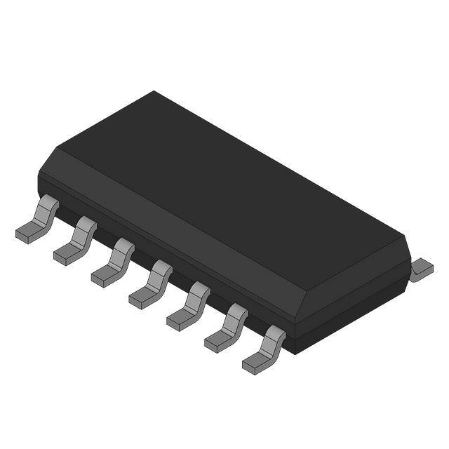
Connection Diagram
DS015009-4
Pinout
DIP & SOIC
© 2001 National Semiconductor Corporation
DS015009
www.national.com
CLC5644 Low Power, Low Cost, Quad Operational Amplifier
July 2001
�CLC5644
Typical Configurations
DS015009-2
Non-Inverting Gain
DS015009-3
Note: Rb provides DC bias for the non-inverting input. Select Rt to yield desired Rin = Rt || Rg.
Inverting Gain
Ordering Information
Package
Temperature Range
Industrial
Part Number
Package
Marking
NSC
Drawing
14-pin plastic DIP
−40˚C to +85˚C
CLC5644IN
CLC5644IN
N14A
14-pin plastic SOIC
−40˚C to +85˚C
CLC5644IM
CLC5644IM
M14A
CLC5644IMX
CLC5644IM
www.national.com
2
�Lead Temperature (soldering 10 sec)
If Military/Aerospace specified devices are required,
please contact the National Semiconductor Sales Office/
Distributors for availability and specifications.
Operating Ratings
Supply Voltage (VCC-VEE)
Output Current
Common-Mode Input Voltage
Maximum Junction Temperature
Storage TemperatureRange
Thermal Resistance
Package
MDIP
SOIC
+14V
95mA
VEE to VCC
+150˚C
−65˚C to +150˚C
+300˚C
(θJC)
60˚C/W
55˚C/W
(θJA)
110˚C/W
125˚C/W
Electrical Characteristics
(AV = +2, Rf =1.65kΩ, RL =100Ω, VS = ± 5V, unless specified)
Parameter
Ambient Temperature
Conditions
Typ
CLC5644IN/IM
Min/Max Ratings
(Note 2)
Units
+25˚C
+25˚C
−40 to
85˚C
AV = 1
170
–
–
MHz
VO < 0.5VPP
VO < 5VPP
125
–
–
MHz
50
–
–
MHz
25
–
–
MHz
Frequency Domain Response
-3dB Bandwidth
−0.1dB Bandwidth
Differential Gain
NTSC, RL = 150Ω
0.04
dB
Differential Phase
NTSC, RL = 150Ω
0.07
dB
0.5V Step
2.7
–
–
ns
Time Domain Response
Rise and Fall Time
5V Step
7
–
–
ns
Settling Time to 0.01%
1V Step
16
–
–
ns
Overshoot
0.5V Step
4
–
–
%
1000
–
–
V/µs
Slew Rate
Distortion And Noise Response
2nd Harmonic Distortion
2VPP,1MHz
−72
–
–
dBc
3rd Harmonic Distortion
2VPP,1MHz
−79
–
–
dBc
Voltage (eni)
> 1MHz
4.5
–
–
nV/
Non-Inverting Current (ibn)
> 1MHz
1.5
–
–
pA/
Inverting Current (ibi)
> 1MHz
10
–
–
pA/
Crosstalk (Input Referred)
10MHz
76
–
–
Equivalent Input Noise
dB
Static, DC Performance
Input Offset Voltage (Note 3)
2.5
7
15
mV
25
–
90
µV/˚C
2
6
10
µA
Average Drift
15
–
80
nA/˚C
Input Bias Current
(Inverting)(Note 3)
2.5
7.5
22
µA
Average Drift
Input Bias Current
(Non-Inverting)(Note 3)
24
–
150
nA/˚C
Power Supply Rejection Ratio
Average Drift
DC
50
46
44
dB
Common Mode Rejection Ratio
DC
50
45
43
dB
Supply Current (per
amplifier)(Note 3)
RL = ∞
2.5
3
3
mA
3
www.national.com
CLC5644
Absolute Maximum Ratings (Note 1)
�(Continued)
(AV = +2, Rf =1.65kΩ, RL =100Ω, VS = ± 5V, unless specified)
Parameter
Conditions
Typ
Min/Max Ratings
(Note 2)
Units
Miscellaneous Performance
Input Resistance (Non-Inverting)
2
1
0.5
MΩ
Input Capacitance
(Non-Inverting)
1
2
2
pF
± 2.2
± 2.8
± 2.0
± 2.6
± 1.4
± 2.5
V
70
50
30
mA
0.2
0.3
0.6
mΩ
Common-Mode Input Range
Output Voltage Range
RL = 150Ω
Output Current
Output Resistance, Closed Loop
DC
V
Note 1: “Absolute Maximum Ratings” are those values beyond which the safety of the device cannot be guaranteed. They are not meant to imply that the devices
should be operated at these limits. The table of “Electrical Characteristics” specifies conditions of device operation.
Note 2: Min/max ratings are based on product characterization and simulation. Individual parameters are tested as noted. Outgoing quality levels are determined
from tested parameters.
Note 3: AJ-level: spec. is 100% tested at +25˚C.
Non-Inverting Frequency Response
Inverting Frequency Response
Gain
Av = +1
Rf = 6.98kΩ
Phase
0
-45
-90
Av = +5
Rf = 499Ω
-135
Av = +10
Rf = 249Ω
-180
-225
1M
10M
45
Av = -2
Rf = 887Ω
Vo = 0.25Vpp
-45
Gain
Phase
-90
Av = -1
Rf = 1.1kΩ
-135
-180
-225
-270
Av = -5
Rf = 422Ω
-315
Av = -10
Rf = 294Ω
-360
-405
100M
1M
Frequency (Hz)
10M
100M
Frequency (Hz)
DS015009-5
Frequency Response vs. RL
DS015009-6
Frequency Response vs. VO
Gain
Phase
0
RL = 1kΩ
RL = 25Ω
Vo = 0.1Vpp
Magnitude (1dB/div)
Phase (deg)
RL = 100Ω
Vo = 5Vpp
-90
-180
-270
Vo = 1Vpp
Vo = 2Vpp
Vo = 4Vpp
-360
1M
10M
100M
-450
1000M
1M
10M
100M
Frequency (Hz)
Frequency (Hz)
DS015009-8
DS015009-7
www.national.com
0
Phase (deg)
Phase (deg)
Av = +2
Rf = 1.65kΩ
Vo = 0.25Vpp
Normalized Magnitude (0.5dB/div)
(AV = +2, Rf = 1.65kΩ, RL = 100Ω, VS = +5V)
Normalized Magnitude (0.5dB/div)
Typical Performance Characteristics
Magnitude (1dB/div)
CLC5644
Electrical Characteristics
4
�(AV = +2, Rf = 1.65kΩ, RL = 100Ω, VS = +5V) (Continued)
2nd & 3rd Harmonic Distortion
2nd & 3rd Harmonic Distortion, RL = 25Ω
-50
-30
Vo = 2Vpp
3rd
RL = 100Ω
-55
2nd
RL = 100Ω
-65
Distortion (dBc)
Distortion (dBc)
3rd = 10MHz
-40
-60
-70
-75
2nd
RL = 1kΩ
-80
3rd
RL = 1kΩ
-85
2nd = 10MHz
-50
3rd = 1MHz
-60
-70
2nd = 1MHz
-90
-95
-80
1M
10M
0
Frequency (Hz)
1
2
Output Amplitude (Vpp)
DS015009-9
2nd & 3rd Harmonic Distortion, RL = 100Ω
DS015009-10
2nd & 3rd Harmonic Distortion, RL = 1kΩ
DS015009-11
Large Signal Pulse Response
Output Voltage (0.1V/div)
Small Signal Pulse Response
DS015009-12
Time (20ns/div)
DS015009-14
DS015009-13
5
www.national.com
CLC5644
Typical Performance Characteristics
�Most Susceptible Channel Pulse Coupling
Channel to Channel Gain Matching
Inactive Channel
Channel 1
Channel 2
Magnitude (0.5dB/div)
Active Channel
Phase (deg)
Inactive Amplitude (10mV/div)
Active Amplitude (0.5V/div)
(AV = +2, Rf = 1.65kΩ, RL = 100Ω, VS = +5V) (Continued)
0
-45
Channel 3
-90
-135
Channel 4
-180
-225
1M
100M
10M
Frequency (Hz)
Time (20ns/div)
DS015009-16
DS015009-15
Equivalent Input Noise
Open-Loop Transimpedance Gain, Z(s)
Noise Voltage (nV/√Hz)
Voltage = 4.5nV/√Hz
Non-Inverting
Current = 1.5pA/√Hz
1
100
1k
10k
100k
1M
10M
1
100M
50
CMRR
PSRR
20
1M
10M
100M
Frequency (Hz)
DS015009-19
www.national.com
160
100
140
Gain
90
120
80
100
Phase
70
80
60
60
50
40
40
20
10k
100k
1M
10M
0
100M
DS015009-18
60
100k
180
110
Frequency (Hz)
PSRR and CMRR
10
10k
120
1k
DS015009-17
30
200
30
Frequency (Hz)
40
130
Phase (degrees)
10
Noise Current (pA/√Hz)
Inverting Current = 10pA/√Hz
10
20 log[|Vo/Ii|/1Ω]
100
100
PSRR, CMRR (dB)
CLC5644
Typical Performance Characteristics
6
�CLC5644
Application Division
• Affects frequency response phase linearity
Layout Considerations
Current Feedback Amplifiers
Some of the key features of current feedback technology
are:
A proper printed circuit layout is essential for achieving high
frequency performance. National provides evaluation boards
for the CLC5644 (CLC730024-DIP, CLC730031-SOIC) and
suggests their use as a guide for high frequency layout and
as an aid for device testing and characterization. General
layout and supply bypassing play major roles in high frequency performance. Follow these steps below as a basis
for high frequency layout:
• Independence of AC bandwidth and voltage gain
• Inherently stable at unity gain
• Adjustable frequency response with Rf
• High slew rate
• Fast settling
Current feedback operation can be described using a simple
equation. The voltage gain for a non-inverting or inverting
current feedback amplifier is approximated by Equation 1.
Vo
Av
=
Vi 1+ R f
Z( jω )
(1)
where:
Av is the closed loop DC voltage gain
Rf is the feedback resistor
Include 6.8µF tantalum and 0.1µF ceramic capacitors on
both supplies.
•
Place the 6.8µF capacitors within 0.75 inches of the
power pins.
•
Place the 0.1µF capacitors less than 0.1 inches from the
power pins.
•
Remove the ground plane under and around the part,
especially near the input and output pins to reduce parasitic capacitance.
•
•
Minimize all trace lengths to reduce series inductances.
Use flush-mount printed circuit board pins for prorotyping, never use high profile DIP sockets.
Active Filter Application Notes
OA-21 Simplified Component Pre-Distortion for High Speed
Active Filters
OA-26 Designing High-Speed Active Filters
OA-27 Low-Sensitivity, Lowpass Filter Design
OA-28 Low-Sensitivity, Bandpass Filter Design with Tuning
Method
OA-29 Low-Sensitivity, Highpass Filter Design with Parasitic
Compensation
Z(jω) is the open loop transimpedance gain
The denominator of Equation 1 is approximately equal to 1 at
low frequencies. Near the −3dB corner frequency, the interaction between Rf and Z(jω) dominates the circuit performance. The value of the feedback resistor has a large affect
on the circuits performance. Increasing Rf has the following
affects:
•
•
•
•
•
Decreases loop gain
Decreases bandwidth
Reduces gain peaking
Lowers pulse response overshoot
7
www.national.com
�CLC5644
Physical Dimensions
inches (millimeters) unless otherwise noted
14-Pin MDIP
NS Package Number N14A
14-Pin SOIC
NS Package Number M14A
www.national.com
8
�CLC5644 Low Power, Low Cost, Quad Operational Amplifier
Notes
LIFE SUPPORT POLICY
NATIONAL’S PRODUCTS ARE NOT AUTHORIZED FOR USE AS CRITICAL COMPONENTS IN LIFE SUPPORT
DEVICES OR SYSTEMS WITHOUT THE EXPRESS WRITTEN APPROVAL OF THE PRESIDENT AND GENERAL
COUNSEL OF NATIONAL SEMICONDUCTOR CORPORATION. As used herein:
1. Life support devices or systems are devices or
systems which, (a) are intended for surgical implant
into the body, or (b) support or sustain life, and
whose failure to perform when properly used in
accordance with instructions for use provided in the
labeling, can be reasonably expected to result in a
significant injury to the user.
National Semiconductor
Corporation
Americas
Email: support@nsc.com
www.national.com
National Semiconductor
Europe
Fax: +49 (0) 180-530 85 86
Email: europe.support@nsc.com
Deutsch Tel: +49 (0) 69 9508 6208
English Tel: +44 (0) 870 24 0 2171
Français Tel: +33 (0) 1 41 91 8790
2. A critical component is any component of a life
support device or system whose failure to perform
can be reasonably expected to cause the failure of
the life support device or system, or to affect its
safety or effectiveness.
National Semiconductor
Asia Pacific Customer
Response Group
Tel: 65-2544466
Fax: 65-2504466
Email: ap.support@nsc.com
National Semiconductor
Japan Ltd.
Tel: 81-3-5639-7560
Fax: 81-3-5639-7507
National does not assume any responsibility for use of any circuitry described, no circuit patent licenses are implied and National reserves the right at any time without notice to change said circuitry and specifications.
�


 工商网监
湘ICP备2023018690号
工商网监
湘ICP备2023018690号
