DRV8801A-Q1
SLVSC79D – JUNE 2014 – REVISEDDRV8801A-Q1
NOVEMBER 2020
SLVSC79D – JUNE 2014 – REVISED NOVEMBER 2020
www.ti.com
DRV8801A-Q1 DMOS Full-Bridge Motor Drivers
1 Features
3 Description
•
•
•
•
•
•
•
•
The DRV8801A-Q1 device provides a versatile motordriver solution with a full H-bridge driver. The device
can drive a brushed DC motor or one winding of a
stepper motor, as well as other devices like solenoids.
A simple PHASE and ENABLE interface allows easy
interfacing to controller circuits.
Qualified for Automotive Applications
Low ON-Resistance (0.83 Ω) Outputs
Low-Power Sleep Mode
100% PWM Duty Cycle Supported
6.5 to 36-V Operating Supply Voltage Range
Thermally Enhanced Surface-Mount Package
Configurable Overcurrent Limit
Protection Features
– VBB Undervoltage Lockout (UVLO)
– Overcurrent Protection (OCP)
– Short-to-Supply Protection
– Short-to-Ground Protection
– Overtemperature Warning (OTW)
– Overtemperature shutdown (OTS)
– Overcurrent and Overtemperature Fault
Conditions Indicated On Pin (nFAULT)
A low-power sleep mode is provided which shuts
down internal circuitry to achieve very low quiescent
current draw. This sleep mode can be set using a
dedicated nSLEEP pin.
Internal
protection
functions
are
provided
undervoltage lockout, overcurrent protection, shortto-supply protection, short-to-ground protection,
overtemperature warning, and overtemperature
shutdown. Overcurrent (including short-to-ground and
short-to-supply) and overtemperature fault conditions
are indicated via an nFAULT pin.
2 Applications
•
•
•
•
The output stages use N-channel power MOSFETs
configured as an H-bridge. The DRV8801A-Q1 device
is capable of peak output currents up to ±2.8 A and
operating voltages up to 36 V. An internal charge
pump generates required gate drive voltages.
Automotive Body Systems
Door Locks
HVAC Actuators
Piezo Alarm
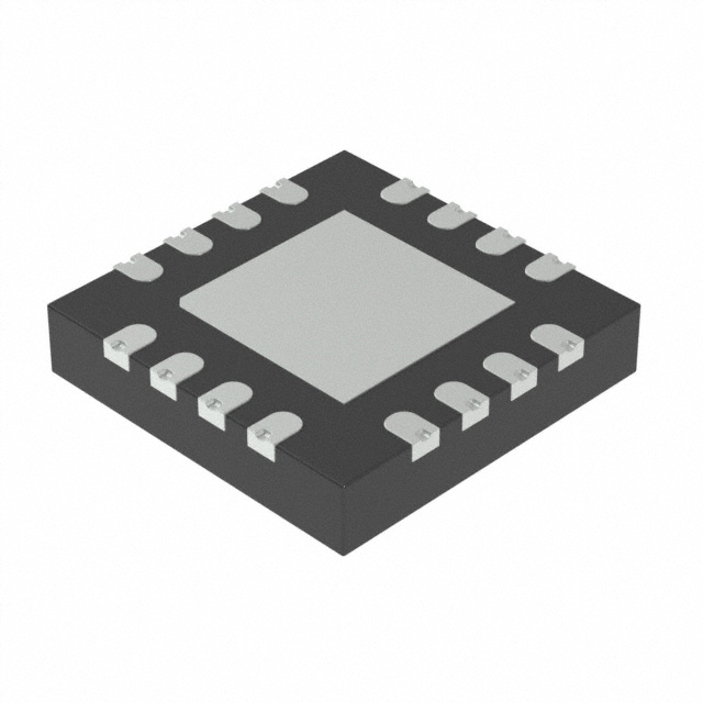
The DRV8801A-Q1 device is packaged in a 16-pin
WQFN package with wettable flanks and exposed
thermal pad (Eco-friendly: RoHS & no Sb/Br).
Device Information
PART NUMBER(1)
DRV8801A-Q1
(1)
PACKAGE
WQFN (16)
BODY SIZE (NOM)
4.00 mm × 4.00 mm
For all available packages, see the orderable addendum at
the end of the datasheet.
6.5 to 36 V
Controller
PH/EN
VPROPI
DRV8801A-Q1
Full-Bridge
Driver
M
nFAULT
Simplified Application Diagram
An©IMPORTANT
NOTICEIncorporated
at the end of this data sheet addresses availability, warranty, changes, use in
safety-critical
applications,
Copyright
2021 Texas Instruments
Submit
Document
Feedback
intellectual property matters and other important disclaimers. PRODUCTION DATA.
Product Folder Links: DRV8801A-Q1
1
�DRV8801A-Q1
www.ti.com
SLVSC79D – JUNE 2014 – REVISED NOVEMBER 2020
Table of Contents
1 Features............................................................................1
2 Applications..................................................................... 1
3 Description.......................................................................1
4 Revision History.............................................................. 2
5 Pin Configuration and Functions...................................3
6 Specifications.................................................................. 4
6.1 Absolute Maximum Ratings........................................ 4
6.2 ESD Ratings............................................................... 4
6.3 Recommended Operating Conditions.........................4
6.4 Thermal Information....................................................5
6.5 Electrical Characteristics.............................................5
6.6 Dissipation Ratings..................................................... 6
6.7 Typical Characteristics................................................ 6
7 Detailed Description........................................................8
7.1 Overview..................................................................... 8
7.2 Functional Block Diagram........................................... 8
7.3 Feature Description.....................................................9
7.4 Device Functional Modes..........................................12
8 Application and Implementation.................................. 13
8.1 Application Information............................................. 13
8.2 Typical Application.................................................... 13
8.3 Parallel Configuration................................................15
9 Power Supply Recommendations................................19
9.1 Bulk Capacitance...................................................... 19
10 Layout...........................................................................20
10.1 Layout Guidelines................................................... 20
10.2 Layout Example...................................................... 20
10.3 Power Dissipation................................................... 20
11 Device and Documentation Support..........................21
11.1 Documentation Support.......................................... 21
11.2 Receiving Notification of Documentation Updates.. 21
11.3 Support Resources................................................. 21
11.4 Community Resources............................................21
11.5 Trademarks............................................................. 21
11.6 Electrostatic Discharge Caution.............................. 21
11.7 Glossary.................................................................. 21
12 Mechanical, Packaging, And Orderable
Information.................................................................... 22
4 Revision History
NOTE: Page numbers for previous revisions may differ from page numbers in the current version.
Changes from Revision C (July 2016) to Revision D (June 2020)
Page
• Improved description for pins CP1, CP2,nFAULT, nSLEEP, VBB and VCP in Pin Functions table.................... 3
• Added entries for VCP and CP2 pins in Absolute Maximum Ratings table........................................................ 4
• Removed incorrect duplicate input logic current entry for ENABLE pin in Electrical Characteristics table.........5
• Added additional information on SENSE pin behavior..................................................................................... 10
• Added equation for VPROPI to help when connecting pin’s output to ADC in Feature Description ................ 11
• Added die temperature estimation equation utilizing junction to ambient thermal impedance in Application and
Implementation section.....................................................................................................................................14
• Added information on using motor driver’s pulse width modulating modes in Application and Implementation
section.............................................................................................................................................................. 14
• Added information on connecting multiple DRV8801-Q1 together to support higher current in Application and
Implementation section.....................................................................................................................................15
Changes from Revision B (June 2016) to Revision C (July 2016)
Page
• Changed the TJ value for some test conditions for the output ON resistance parameter in the Electrical
Characteristics ................................................................................................................................................... 5
• Added the Documentation Support, Receiving Notification of Documentation Updates, and Community
Resources sections ......................................................................................................................................... 21
Changes from Revision A (September 2014) to Revision B (June 2016)
Page
• Changed the value of TJ from 125°C to 25°C in the test condition (source driver, IO = –2.8 A, VBB = 8 to 36 V)
for the output ON resistance parameter............................................................................................................. 5
• Added the UVLO hysteresis parameter in the Electrical Characteristics table................................................... 5
• Added MIN and MAX values for the overcurrent retry time parameter in the Electrical Characteristics table ....
5
• Updated the Functional Block Diagram ............................................................................................................. 8
• Added tpd to the Overcurrent Control Timing image......................................................................................... 10
2
Submit Document Feedback
Copyright © 2021 Texas Instruments Incorporated
Product Folder Links: DRV8801A-Q1
�DRV8801A-Q1
www.ti.com
SLVSC79D – JUNE 2014 – REVISED NOVEMBER 2020
Changes from Revision * (June 2014) to Revision A (September 2014)
Page
• Added TYPE column to the Pin Functions table ................................................................................................3
• Updated the Overcurrent Control Timing image............................................................................................... 10
12
GND
11
CP2
10
CP1
MODE_1
nFAULT
VPROPI
VCP
15
14
13
9
8
4
VBB
ENABLE
Pad
7
3
SENSE
nSLEEP
Thermal
6
2
OUTA
GND
5
1
MODE_2
PHASE
16
5 Pin Configuration and Functions
OUTB
Not to scale
Figure 5-1. RMJ Package 16-Pin WQFN With Thermal Pad Top View
Table 5-1. Pin Functions
PIN
NAME
NO.
TYPE
CP1
10
—
CP2
11
—
ENABLE
4
I
GND
2
12
PWR
DESCRIPTION
Charge pump switching node. Connect a X7R, 0.1-μF, VBB-rated ceramic capacitor from CP1 to CP2.
Enables OUTA and OUTB drivers
Ground
MODE 1
16
I
Mode logic input
MODE 2
5
I
Mode 2 logic input
nFAULT
15
OD
Fault indication. Pulled logic low with fault condition; open-drain output requires an external pullup
resistor.
nSLEEP
3
I
Sleep mode input. Logic high to enable device; logic low to enter low-power sleep mode; internal
pulldown resistor.
OUTA
6
O
DMOS full-bridge output positive. H-Bridge output A
OUTB
9
O
DMOS full-bridge output negative. H-Bridge output B
PHASE
1
I
Phase logic input for direction control
SENSE
7
IO
VBB
8
PWR
VCP
13
—
Charge pump reservoir capacitor pin. Connect a X7R, 0.1-μF, 16-V ceramic capacitor to VBB.
VPROPI
14
O
Winding current proportional voltage output
—
Exposed pad for thermal dissipation; connect to GND pins.
Thermal pad
Sense power return
Driver supply voltage. Bypass to GND with 0.1-μF ceramic capacitors plus a bulk capacitor rated for
VBB.
Submit Document Feedback
Copyright © 2021 Texas Instruments Incorporated
Product Folder Links: DRV8801A-Q1
3
�DRV8801A-Q1
www.ti.com
SLVSC79D – JUNE 2014 – REVISED NOVEMBER 2020
6 Specifications
6.1 Absolute Maximum Ratings
over operating free-air temperature range (unless otherwise noted)(1)
MIN
MAX
UNIT
Power supply voltage(2)
VBB
–0.3
40
V
Charge pump voltage
VCP and CP2
–0.3
VBB +17
V
Digital pin voltage
PHASE, ENABLE, MODE1, MODE2, nSLEEP, nFAULT
–0.3
7
V
VBB to OUTx voltage
OUTA and OUTB
–0.3
36
V
OUTx to GND voltage
OUTA and OUTB
–0.3
36
V
–0.5
Sense pin voltage
SENSE
H-bridge output current
OUTA, OUTB, and SENSE
VPROPI pin voltage
VPROPI
–0.3
Maximum junction temperature, TJ
Storage temperature, Tstg
(1)
(2)
–40
0.5
V
2.8
A
3.6
V
150
°C
125
°C
Stresses beyond those listed under Absolute Maximum Ratings may cause permanent damage to the device. These are stress
ratings only, which do not imply functional operation of the device at these or any other conditions beyond those indicated under
Recommended Operating Conditions. Exposure to absolute-maximum-rated conditions for extended periods may affect device
reliability.
All voltage values are with respect to network ground terminal.
6.2 ESD Ratings
VALUE
Human-body model (HBM), per AEC Q100-002(1)
V(ESD)
(1)
Electrostatic
discharge
Charged-device model (CDM), per AEC Q100-011
UNIT
±2000
All pins
±500
Corner pins (1, 4, 5, 8, 9, 12,
13, and 16)
±750
V
AEC Q100-002 indicates that HBM stressing shall be in accordance with the ANSI/ESDA/JEDEC JS-001 specification.
6.3 Recommended Operating Conditions
MIN
4
VBB
Power supply voltage
VCC
Logic supply voltage
ƒ(PWM)
IO
TA
Ambient temperature
MAX
UNIT
6.5
36
V
0
5.5
V
Applied PWM signal (PHASE and ENABLE)
0
100
kHz
H-bridge peak output current
0
2.8
A
–40
125
°C
Submit Document Feedback
Copyright © 2021 Texas Instruments Incorporated
Product Folder Links: DRV8801A-Q1
�DRV8801A-Q1
www.ti.com
SLVSC79D – JUNE 2014 – REVISED NOVEMBER 2020
6.4 Thermal Information
DRV8801A-Q1
THERMAL
METRIC(1)
UNIT
RMJ (WQFN)
16 PINS
RθJA
Junction-to-ambient thermal resistance
36.8
°C/W
RθJCtop
Junction-to-case (top) thermal resistance
43.4
°C/W
RθJB
Junction-to-board thermal resistance
14.7
°C/W
ψJT
Junction-to-top characterization parameter
0.7
°C/W
ψJB
Junction-to-board characterization parameter
14.7
°C/W
RθJCbot
Junction-to-case (bottom) thermal resistance
4.3
°C/W
(1)
For more information about traditional and new thermal metrics, see the Semiconductor and IC Package Thermal Metrics application
report.
6.5 Electrical Characteristics
TA = 25°C, over recommended operating conditions (unless otherwise noted)
PARAMETER
TEST CONDITIONS
MIN
TYP
MAX
UNIT
POWER SUPPLIES (VBB)
VBB
VBB operating supply voltage
IBB
VBB operating supply current
IBB(Q)
VBB sleep-mode supply current
6.5
ƒPWM < 50 kHz
36
6
Charge pump on, Outputs disabled
mA
3.2
nSLEEP = 0, TJ = 25°C
V
10
μA
CONTROL INPUTS (PHASE, ENABLE, MODE1, MODE2, nSLEEP)
VIL
Input logic low voltage
VIH
Input logic high voltage
IIL
Input logic low current
IIH
Input logic high current
IIL
Input logic low current
IIH
Input logic high current
VIL
Input logic low voltage
VIH
Input logic high voltage
IIL
Input logic low current
IIH
Input logic high current
0.8
PHASE, ENABLE
MODE1, MODE2
PHASE,
MODE1, MODE2
ENABLE
2
VI = 0.8 V
–20
≤ –2
20