Product
Folder
Sample &
Buy
Support &
Community
Tools &
Software
Technical
Documents
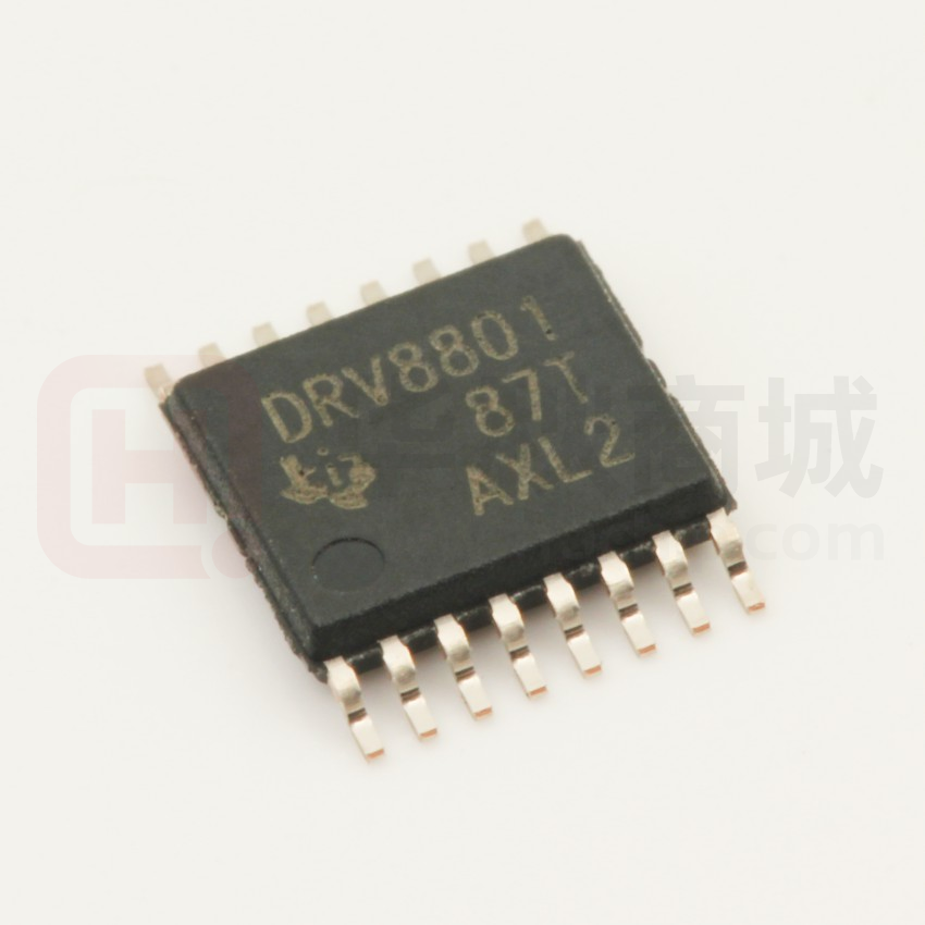
DRV8800, DRV8801
SLVS855J – JULY 2008 – REVISED MARCH 2015
DRV880x DMOS Full-Bridge Motor Drivers
1 Features
3 Description
•
•
•
•
•
•
•
The DRV880x provides a versatile motor driver
solution with a variety of capabilities. The device
contains a full H-bridge which can be used to drive a
brushed DC motor, one winding of a stepper motor,
or other devices such as solenoids. A simple PHASEENABLE interface allows easy interfacing to
controller circuits.
1
H-Bridge Motor Driver
Low RDS(on) MOSFETs (0.4-Ω Typical)
Low-Power Sleep Mode
100% PWM Supported
8-V to 36-V Operating Supply Voltage Range
Thermally Enhanced Surface-Mount Package
Protection Features:
– VBB Undervoltage Lockout (UVLO)
– Charge Pump Undervoltage (CPUV)
– Overcurrent Protection (OCP)
– Short-to-Supply Protection
– Short-to-Ground Protection
– Overtemperature Warning (OTW)
– Overtemperature Shutdown (OTS)
– Fault Condition Indication Pin (nFAULT)
2 Applications
•
•
•
Printers
Industrial Automation
Robotics
The output stages use N-channel power MOSFETs
configured as an H-bridge. The DRV880xis capable
of peak output currents up to ±2.8 A and operating
voltages up to 36 V. An internal charge pump
generates the needed gate drive voltages.
A low-power sleep mode is provided which shuts
down internal circuitry to achieve a very low
quiescent current draw. This sleep mode can be set
using a dedicated nSLEEP pin.
Internal protection functions are provided for
undervoltage, charge pump fault, overcurrent, shortto-supply, short-to-ground, and overtemperature.
Fault conditions are indicated through the nFAULT
pin.
The DRV880x is packaged in a 16-pin WQFN
package with PowerPAD™ (Eco-friendly: RoHS & no
Sb/Br).
Device Information(1)
PART NUMBER
DRV8800
DRV8801
PACKAGE
BODY SIZE (NOM)
HTSSOP (16)
5.00 mm × 4.40 mm
WQFN (16)
4.00 mm × 4.00 mm
HTSSOP (16)
5.00 mm × 4.40 mm
WQFN (16)
4.00 mm × 4.00 mm
(1) For all available packages, see the orderable addendum at
the end of the data sheet.
4 Simplified Schematic
8 V to 36 V
Controller
PHASE
DRV8800/
DRV8801
ENABLE
nSLEEP
Brushed DC
Motor Driver
M
nFAULT
Protection
1
An IMPORTANT NOTICE at the end of this data sheet addresses availability, warranty, changes, use in safety-critical applications,
intellectual property matters and other important disclaimers. PRODUCTION DATA.
�DRV8800, DRV8801
SLVS855J – JULY 2008 – REVISED MARCH 2015
www.ti.com
Table of Contents
1
2
3
4
5
6
7
8
9
Features ..................................................................
Applications ...........................................................
Description .............................................................
Simplified Schematic.............................................
Revision History.....................................................
Pin Configuration and Functions .........................
Specifications.........................................................
1
1
1
1
2
3
5
7.1
7.2
7.3
7.4
7.5
7.6
5
5
5
5
6
7
Absolute Maximum Ratings .....................................
ESD Ratings..............................................................
Recommended Operating Conditions.......................
Thermal Information ..................................................
Electrical Characteristics...........................................
Typical Characteristics ..............................................
Parameter Measurement Information .................. 8
Detailed Description ............................................ 10
9.1 Overview ................................................................. 10
9.2 Functional Block Diagrams ..................................... 10
9.3 Feature Description................................................. 11
9.4 Device Functional Modes........................................ 13
10 Application and Implementation........................ 15
10.1 Application Information.......................................... 15
10.2 Typical Application ................................................ 15
11 Power Supply Recommendations ..................... 19
11.1 Bulk Capacitance .................................................. 19
12 Layout................................................................... 20
12.1 Layout Guidelines ................................................. 20
12.2 Layout Example .................................................... 20
13 Device and Documentation Support ................. 22
13.1
13.2
13.3
13.4
Related Links ........................................................
Trademarks ...........................................................
Electrostatic Discharge Caution ............................
Glossary ................................................................
22
22
22
22
14 Mechanical, Packaging, and Orderable
Information ........................................................... 22
5 Revision History
Changes from Revision I (January 2014) to Revision J
•
Page
Added ESD Ratings table, Feature Description section, Device Functional Modes, Application and Implementation
section, Power Supply Recommendations section, Layout section, Device and Documentation Support section, and
Mechanical, Packaging, and Orderable Information section ................................................................................................. 5
Changes from Revision H (November 2013) to Revision I
Page
•
Added IOCP to ELECTRICAL CHARACTERISTICS ................................................................................................................ 6
•
Changed Figure 5................................................................................................................................................................... 9
Changes from Revision G (October 2013) to Revision H
Page
•
Changed maximum junction temperature from 190°C to 150°C ............................................................................................ 5
•
Changed VTRP description/test conditions ............................................................................................................................ 6
•
Changed Protection Circuitry section ..................................................................................................................................... 6
•
Changed Note in SENSE section ......................................................................................................................................... 13
2
Submit Documentation Feedback
Copyright © 2008–2015, Texas Instruments Incorporated
Product Folder Links: DRV8800 DRV8801
�DRV8800, DRV8801
www.ti.com
SLVS855J – JULY 2008 – REVISED MARCH 2015
6 Pin Configuration and Functions
DRV8800 RTY Package
16-Pin WQFN
Top View
GND
GND
2
11
CP2
nFAULT
VPROPI
VCP
14
13
VCP
13
12
15
VREG
14
1
MODE 1
nFAULT
15
PHASE
16
MODE
16
DRV8801 RTY Package
16-Pin WQFN
Top View
PHASE
1
12
GND
GND
2
11
CP2
PowerPAD
PowerPAD
OUT-
DRV8800 PWP Package
16-Pin HTSSOP
Top View
8
9
VBB
4
7
ENABLE
SENSE
CP1
6
10
OUT+
3
5
nSLEEP
MODE 2
8
OUT-
VBB
9
7
4
SENSE
ENABLE
6
CP1
OUT+
10
5
3
NC
nSLEEP
DRV8801 PWP Package
16-Pin HTSSOP
Top View
nFAULT
1
16
NC
MODE
2
15
VREG
PHASE
3
14
VCP
GND
4
13
GND
nSLEEP
5
12
CP2
ENABLE
6
11
CP1
OUT+
7
10
OUT-
SENSE
8
9
VBB
PowerPAD
nFAULT
1
16
MODE 2
MODE 1
2
15
VPROPI
PHASE
3
14
VCP
GND
4
13
GND
PowerPAD
nSLEEP
5
12
CP2
ENABLE
6
11
CP1
OUT+
7
10
OUT-
SENSE
8
9
VBB
Copyright © 2008–2015, Texas Instruments Incorporated
Product Folder Links: DRV8800 DRV8801
Submit Documentation Feedback
3
�DRV8800, DRV8801
SLVS855J – JULY 2008 – REVISED MARCH 2015
www.ti.com
Pin Functions
PIN
NAME
DRV8800
DRV8801
I/O
DESCRIPTION
WQFN
HTSSOP
WQFN
HTSSOP
CP1
10
11
10
11
P
Charge pump switching node. Connect a 0.1-μF X7R ceramic
capacitor rated for VBB between CP1 and CP2.
CP2
11
12
11
12
P
Charge pump switching node. Connect a 0.1-μF X7R ceramic
capacitor rated for VBB between CP1 and CP2.
ENABLE
4
6
4
6
I
Enable logic input. Set high to enable the H-bridge.
GND
2
4
2
4
P
Device ground
MODE
16
2
—
—
I
Mode logic input
MODE 1
—
—
16
2
I
Mode logic input
MODE 2
—
—
5
16
I
Mode 2 logic input
NC
5
16
—
—
NC
No connect
nFAULT
15
1
15
1
OD
Pulled logic low in FAULT condition. Open-drain output
requires external pullup.
nSLEEP
3
5
3
5
I
Sleep logic input. Set low to enter low-power sleep mode.
OUT+
6
7
6
7
O
DMOS H-bridge output. Connect to motor terminal.
OUT-
9
10
9
10
O
DMOS H-bridge output. Connect to motor terminal.
PHASE
1
3
1
3
I
WQFN Package: Phase logic input for direction control.
HTSSOP Package: Phase logic input. Controls the direction of
the H-bridge.
VBB
8
9
8
9
P
Connect to motor power supply. Bypass to ground with 0.1-μF
ceramic capacitor and appropriate bulk capacitance rated for
VBB.
VCP
13
14
13
14
P
Charge pump output. Connect a 0.1-µF 16-V ceramic capacitor
between VCP and VBB.
VREG
14
15
—
—
P
Regulated voltage.
VPROPI
—
—
14
15
O
Voltage output proportional to winding current.
PowerPAD
—
—
—
—
—
Exposed pad for thermal dissipation. Connect to ground.
4
Submit Documentation Feedback
Copyright © 2008–2015, Texas Instruments Incorporated
Product Folder Links: DRV8800 DRV8801
�DRV8800, DRV8801
www.ti.com
SLVS855J – JULY 2008 – REVISED MARCH 2015
7 Specifications
7.1 Absolute Maximum Ratings
over operating free-air temperature range (unless otherwise noted) (1)
VBB
VSense
Load supply voltage (2)
MIN
MAX
UNIT
–0.3
40
V
Output current
–2.8
2.8
A
Sense voltage
–500
500
mV
36
V
36
V
7
V
VBB to OUTx
OUTx to SENSE
VDD
Logic input voltage (2)
–0.3
Continuous total power dissipation
TA
Operating free-air temperature
TJ
Maximum junction temperature
Tstg
Storage temperature
(1)
(2)
See Thermal Information
–40
–40
85
°C
150
°C
125
°C
Stresses beyond those listed under Absolute Maximum Ratings may cause permanent damage to the device. These are stress ratings
only, and functional operation of the device at these or any other conditions beyond those indicated under Recommended Operating
Conditions is not implied. Exposure to absolute-maximum-rated conditions for extended periods may affect device reliability.
All voltage values are with respect to network ground terminal.
7.2 ESD Ratings
VALUE
V(ESD)
(1)
(2)
Electrostatic discharge
Human body model (HBM), per ANSI/ESDA/JEDEC JS-001, all pins (1)
±2000
Charged device model (CDM), per JEDEC specification JESD22-C101, all
pins (2)
±500
UNIT
V
JEDEC document JEP155 states that 500-V HBM allows safe manufacturing with a standard ESD control process.
JEDEC document JEP157 states that 250-V CDM allows safe manufacturing with a standard ESD control process.
7.3 Recommended Operating Conditions
VIN
Input voltage, VBB
TA
Operating free-air temperature
MIN
NOM
MAX
8
32
38
V
85
°C
–40
UNIT
7.4 Thermal Information
DRV880x
THERMAL METRIC (1)
RTY (WQFN)
PWP (HTSSOP)
16 PINS
16 PINS
RθJA
Junction-to-ambient thermal resistance
38.1
43.9
RθJC(top)
Junction-to-case (top) thermal resistance
36.7
30.8
RθJB
Junction-to-board thermal resistance
16.1
25.3
ψJT
Junction-to-top characterization parameter
0.3
1.1
ψJB
Junction-to-board characterization parameter
16.2
25
RθJC(bot)
Junction-to-case (bottom) thermal resistance
4.1
5.6
(1)
UNIT
°C/W
For more information about traditional and new thermal metrics, see the IC Package Thermal Metrics application report, SPRA953.
Copyright © 2008–2015, Texas Instruments Incorporated
Product Folder Links: DRV8800 DRV8801
Submit Documentation Feedback
5
�DRV8800, DRV8801
SLVS855J – JULY 2008 – REVISED MARCH 2015
www.ti.com
7.5 Electrical Characteristics
over recommended operating conditions (unless otherwise noted)
PARAMETER
TEST CONDITIONS
MIN
fPWM < 50 kHz
IBB
Motor supply current
TYP
6
Charge pump on, Outputs disabled
10
2
PHASE, ENABLE,
MODE input voltage
VIL
VIH
0.8
2.7
nSLEEP input voltage
VIL
IIH
PHASE, MODE input current
IIL
IIH
ENABLE input current
IIL
IIH
nSLEEP input current
IIL
0.8
VIN = 2 V
很抱歉,暂时无法提供与“DRV8801PWPR”相匹配的价格&库存,您可以联系我们找货
免费人工找货- 国内价格
- 1+5.39000
- 10+4.41000
- 30+3.91020
- 100+3.42020