Product
Folder
Sample &
Buy
Support &
Community
Tools &
Software
Technical
Documents
DRV8835
SLVSB18H – MARCH 2012 – REVISED AUGUST 2016
DRV8835 Dual Low-Voltage H-Bridge IC
1 Features
3 Description
•
The DRV8835 provides an integrated motor driver
solution for cameras, consumer products, toys, and
other low-voltage or battery-powered motion control
applications. The device has two H-bridge drivers,
and drives two DC motors or one stepper motor, as
well as other devices like solenoids. The output driver
block for each consists of N-channel power
MOSFETs configured as an H-bridge to drive the
motor winding. An internal charge pump generates
gate drive voltages.
1
•
•
•
•
•
•
•
Dual-H-Bridge Motor Driver
– Capable of Driving Two DC Motors or One
Stepper Motor
– Low-MOSFET ON-Resistance:
HS + LS 305 mΩ
1.5-A Maximum Drive Current Per H-Bridge
Configure Bridges Parallel for 3-A Drive Current
Separate Motor and Logic-Supply Pins:
– 0-V to 11-V Motor-Operating Supply-Voltage
– 2-V to 7-V Logic Supply-Voltage
Separate Logic and Motor Power Supply Pins
Flexible PWM or PHASE/ENABLE Interface
Low-Power Sleep Mode With 95-nA Maximum
Supply Current
Tiny 2.00-mm × 3.00-mm WSON Package
2 Applications
•
The DRV8835 supplies up to 1.5-A of output current
per H-bridge and operates on a motor power supply
voltage from 0 V to 11 V, and a device power supply
voltage of 2 V to 7 V.
PHASE/ENABLE and IN/IN interfaces are compatible
with industry-standard devices.
Internal shutdown functions are provided for
overcurrent protection, short circuit protection,
undervoltage lockout, and overtemperature.
The DRV8835 is packaged in a tiny 12-pin WSON
package (Eco-friendly: RoHS and no Sb/Br).
Battery-Powered:
– Cameras
– DSLR Lenses
– Consumer Products
– Toys
– Robotics
– Medical Devices
Device Information(1)
PART NUMBER
DRV8835
PACKAGE
WSON (12)
BODY SIZE (NOM)
2.00 mm × 3.00 mm
(1) For all available packages, see the orderable addendum at
the end of the data sheet.
Simplified Schematic
VCC = 2 V to 7 V
VM = 0 V to 11 V
Controller
PWM
DRV8835
+
M
1.5 A
±
Stepper or
Brushed DC
Motor Driver
+
±
1.5 A
Copyright © 2016, Texas Instruments Incorporated
1
An IMPORTANT NOTICE at the end of this data sheet addresses availability, warranty, changes, use in safety-critical applications,
intellectual property matters and other important disclaimers. PRODUCTION DATA.
�DRV8835
SLVSB18H – MARCH 2012 – REVISED AUGUST 2016
www.ti.com
Table of Contents
1
2
3
4
5
6
7
Features ..................................................................
Applications ...........................................................
Description .............................................................
Revision History.....................................................
Pin Configuration and Functions .........................
Specifications.........................................................
1
1
1
2
4
5
6.1
6.2
6.3
6.4
6.5
6.6
6.7
5
5
5
5
6
7
8
Absolute Maximum Ratings ......................................
ESD Ratings..............................................................
Recommended Operating Conditions.......................
Thermal Information ..................................................
Electrical Characteristics...........................................
Timing Requirements ................................................
Typical Characteristics ..............................................
Detailed Description .............................................. 9
7.1
7.2
7.3
7.4
Overview ................................................................... 9
Functional Block Diagram ......................................... 9
Feature Description................................................. 10
Device Functional Modes........................................ 10
8
Application and Implementation ........................ 12
8.1 Application Information............................................ 12
8.2 Typical Application ................................................. 12
9
Power Supply Recommendations...................... 14
9.1 Bulk Capacitance .................................................... 14
9.2 Power Supplies and Input Pins ............................... 14
10 Layout................................................................... 15
10.1 Layout Guidelines ................................................. 15
10.2 Layout Example .................................................... 15
10.3 Thermal Considerations ........................................ 15
11 Device and Documentation Support ................. 17
11.1
11.2
11.3
11.4
11.5
11.6
Documentation Support ........................................
Receiving Notification of Documentation Updates
Community Resources..........................................
Trademarks ...........................................................
Electrostatic Discharge Caution ............................
Glossary ................................................................
17
17
17
17
17
17
12 Mechanical, Packaging, and Orderable
Information ........................................................... 17
4 Revision History
NOTE: Page numbers for previous revisions may differ from page numbers in the current version.
Changes from Revision G (May 2016) to Revision H
Page
•
Changed the value of the capacitor on the VM pin from 10 µF to 0.1 µF in the Parallel Mode Connections figure............ 12
•
Added one capacitor to the VM pin and updated the value of the existing capacitor on the VM pin in the Layout
Example................................................................................................................................................................................ 15
•
Deleted references to TI's PowerPAD package and updated it with thermal pad where applicable ................................... 16
•
Added the Receiving Notification of Documentation Updates section ................................................................................ 17
Changes from Revision F (April 2016) to Revision G
•
Changed the Layout Guidelines to clarify the guidelines for the VM pin ............................................................................. 15
Changes from Revision E (December 2015) to Revision F
•
2
Page
Deleted nFAULT from the Simplified Schematic in the Description section ......................................................................... 1
Changes from Revision D (January 2014) to Revision E
•
Page
Page
Added ESD Ratings table, Feature Description section, Device Functional Modes, Application and Implementation
section, Power Supply Recommendations section, Layout section, Device and Documentation Support section, and
Mechanical, Packaging, and Orderable Information section .................................................................................................. 1
Submit Documentation Feedback
Copyright © 2012–2016, Texas Instruments Incorporated
Product Folder Links: DRV8835
�DRV8835
www.ti.com
SLVSB18H – MARCH 2012 – REVISED AUGUST 2016
Changes from Revision C (September 2013) to Revision D
Page
•
Changed Features bullet ........................................................................................................................................................ 1
•
Changed motor supply voltage range in Description section ................................................................................................. 1
•
Changed Motor power supply voltage range in Recommended Operating Conditions ......................................................... 5
•
Added tOCR and tDEAD parameters to Electrical Characteristics .............................................................................................. 6
•
Added paragraph to Power Supplies and Input Pins section ............................................................................................... 14
Submit Documentation Feedback
Copyright © 2012–2016, Texas Instruments Incorporated
Product Folder Links: DRV8835
3
�DRV8835
SLVSB18H – MARCH 2012 – REVISED AUGUST 2016
www.ti.com
5 Pin Configuration and Functions
DSS Package
12-Pin WSON With Exposed Thermal Pad
Top View
VM
AOUT1
AOUT2
BOUT1
BOUT2
GND
1
12
2
11
3
GND
Thermal
pad
4
10
9
5
8
6
7
VCC
MODE
AIN1 / APHASE
AIN2 / AENBL
BIN1 / BPHASE
BIN2 / BENBL
Pin Functions
PIN
NAME
NO.
I/O (1)
DESCRIPTION
EXTERNAL COMPONENTS OR
CONNECTIONS
POWER AND GROUND
GND, Thermal
pad
6
—
Device ground
VM
1
—
Motor supply
Bypass to GND with a 0.1-μF (minimum)
ceramic capacitor
VCC
12
—
Device supply
Bypass to GND with a 0.1-μF (minimum)
ceramic capacitor
MODE
11
I
Input mode select
Logic low selects IN/IN mode
Logic high selects PH/EN mode
Internal pulldown resistor
AIN1/APHASE
10
I
Bridge A input 1/PHASE input
IN/IN mode: Logic high sets AOUT1 high
PH/EN mode: Sets direction of H-bridge A
Internal pulldown resistor
AIN2/AENBL
9
I
Bridge A input 2/ENABLE input
IN/IN mode: Logic high sets AOUT2 high
PH/EN mode: Logic high enables H-bridge A
Internal pulldown resistor
BIN1/BPHASE
8
I
Bridge B input 1/PHASE input
IN/IN mode: Logic high sets BOUT1 high
PH/EN mode: Sets direction of H-bridge B
Internal pulldown resistor
BIN2/BENBL
7
I
Bridge B input 2/ENABLE input
IN/IN mode: Logic high sets BOUT2 high
PH/EN mode: Logic high enables H-bridge B
Internal pulldown resistor
AOUT1
2
O
Bridge A output 1
AOUT2
3
O
Bridge A output 2
BOUT1
4
O
Bridge B output 1
BOUT2
5
O
Bridge B output 2
CONTROL
OUTPUT
(1)
4
Connect to motor winding A
Connect to motor winding B
Directions: I = input, O = output
Submit Documentation Feedback
Copyright © 2012–2016, Texas Instruments Incorporated
Product Folder Links: DRV8835
�DRV8835
www.ti.com
SLVSB18H – MARCH 2012 – REVISED AUGUST 2016
6 Specifications
6.1 Absolute Maximum Ratings
(1) (2)
See
MIN
MAX
UNIT
Power supply voltage, VM
–0.3
12
V
Power supply voltage, VCC
–0.3
7
V
Digital input pin voltage
–0.5
VCC + 0.5
V
Peak motor drive output current
Internally limited
Continuous motor drive output current per H-bridge
(3)
A
–1.5
1.5
A
TJ
Operating junction temperature
–40
150
°C
Tstg
Storage temperature
–60
150
°C
(1)
(2)
(3)
Stresses beyond those listed under Absolute Maximum Ratings may cause permanent damage to the device. These are stress ratings
only, which do not imply functional operation of the device at these or any other conditions beyond those indicated under Recommended
Operating Conditions. Exposure to absolute-maximum-rated conditions for extended periods may affect device reliability.
All voltage values are with respect to network ground terminal.
Power dissipation and thermal limits must be observed.
6.2 ESD Ratings
VALUE
V(ESD)
(1)
(2)
Electrostatic
discharge
Human-body model (HBM), per ANSI/ESDA/JEDEC JS-001
(1)
UNIT
±2000
Charged-device model (CDM), per JEDEC specification JESD22-C101 (2)
V
±1500
JEDEC document JEP155 states that 500-V HBM allows safe manufacturing with a standard ESD control process.
JEDEC document JEP157 states that 250-V CDM allows safe manufacturing with a standard ESD control process.
6.3 Recommended Operating Conditions
TA = 25°C (unless otherwise noted)
MIN
VCC
Device power supply voltage
2
VM
Motor power supply voltage
VIN
Logic level input voltage
IOUT
ƒPWM
(1)
NOM
MAX
UNIT
7
V
0
11
V
0
VCC
V
H-bridge output current (1)
0
1.5
A
Externally applied PWM frequency
0
250
kHz
Power dissipation and thermal limits must be observed.
6.4 Thermal Information
DRV8835
THERMAL METRIC (1)
DSS (WSON)
UNIT
12 PINS
RθJA
Junction-to-ambient thermal resistance
RθJC(top)
Junction-to-case (top) thermal resistance
50.4
°C/W
58
RθJB
°C/W
Junction-to-board thermal resistance
19.9
°C/W
ψJT
Junction-to-top characterization parameter
0.9
°C/W
ψJB
Junction-to-board characterization parameter
20
°C/W
RθJC(bot)
Junction-to-case (bottom) thermal resistance
6.9
°C/W
(1)
For more information about traditional and new thermal metrics, see the Semiconductor and IC Package Thermal Metrics application
report.
Submit Documentation Feedback
Copyright © 2012–2016, Texas Instruments Incorporated
Product Folder Links: DRV8835
5
�DRV8835
SLVSB18H – MARCH 2012 – REVISED AUGUST 2016
www.ti.com
6.5 Electrical Characteristics
TA = 25°C, VM = 5 V, VCC = 3 V (unless otherwise noted)
PARAMETER
TEST CONDITIONS
MIN
TYP
MAX
UNIT
POWER SUPPLY
IVM
VM operating supply current
IVMQ
VM sleep mode supply current
IVCC
VCC operating supply current
VCC undervoltage lockout
voltage
VUVLO
No PWM, no load
50 kHz PWM, no load
85
200
650
2000
VM = 2 V, VCC = 0 V, all inputs 0 V
5
VM = 5 V, VCC = 0 V, all inputs 0 V
10
95
450
2000
VCC rising
2
VCC falling
1.9
µA
nA
µA
V
LOGIC-LEVEL INPUTS
VIL
Input low voltage
VIH
Input high voltage
IIL
Input low current
VIN = 0
IIH
Input high current
VIN = 3.3 V
RPD
Pulldown resistance
0.3 × VCC
V
5
μA
0.5 × VCC
V
–5
50
100
μA
kΩ
H-BRIDGE FETS
RDS(ON)
IOFF
HS + LS FET on resistance
VCC = 3 V, VM = 3 V, I
TJ = 25°C
O
= 800 mA,
VCC = 5 V, VM = 5 V, I
TJ = 25°C
O
= 800 mA,
370
420
305
355
mΩ
OFF-state leakage current
±200
nA
PROTECTION CIRCUITS
IOCP
Overcurrent protection trip level
tDEG
Overcurrent de-glitch time
1
µs
tOCR
Overcurrent protection retry time
1
ms
tDEAD
Output dead time
tTSD
Thermal shutdown temperature
6
1.6
3.5
100
Die temperature
Submit Documentation Feedback
150
160
A
ns
180
°C
Copyright © 2012–2016, Texas Instruments Incorporated
Product Folder Links: DRV8835
�DRV8835
www.ti.com
SLVSB18H – MARCH 2012 – REVISED AUGUST 2016
6.6 Timing Requirements
TA = 25°C, VM = 5 V, VCC = 3 V, RL = 20 Ω
NO.
MIN
MAX
UNIT
1
t1
Delay time, xPHASE high to xOUT1 low
300
ns
2
t2
Delay time, xPHASE high to xOUT2 high
200
ns
3
t3
Delay time, xPHASE low to xOUT1 high
200
ns
4
t4
Delay time, xPHASE low to xOUT2 low
300
ns
5
t5
Delay time, xENBL high to xOUTx high
200
ns
6
t6
Delay time, xENBL high to xOUTx low
300
ns
7
t7
Output enable time
300
ns
8
t8
Output disable time
300
ns
9
t9
Delay time, xINx high to xOUTx high
160
ns
10
t10
Delay time, xINx low to xOUTx low
160
ns
11
tR
Output rise time
30
188
ns
12
tF
Output fall time
30
188
ns
xENBL
IN1
xPHASE
IN2
7
9
8
3
5
OUT1
xOUT1
z
z
10
1
xOUT2
6
5
4
6
OUT2
2
z
z
IN/IN mode
PHASE/ENBL mode
80%
80%
OUTx
20%
20%
11
12
Figure 1. Timing Requirements
Submit Documentation Feedback
Copyright © 2012–2016, Texas Instruments Incorporated
Product Folder Links: DRV8835
7
�DRV8835
SLVSB18H – MARCH 2012 – REVISED AUGUST 2016
www.ti.com
0.65
0.6
0.55
0.5
0.45
0.4
0.35
0.3
0.25
0.2
0.15
0.1
0.05
0
-40
0.5
VCC = 0 V
-40qC
25qC
85qC
0.45
Sleep Current, IVMQ (uA)
VM Operating Current (IVMX) (mA)
6.7 Typical Characteristics
50 kHz, no load
VCC = 2, VM = 2
VCC = 3, VM = 5
VCC = 7, VM = 11
0.4
0.35
0.3
0.25
0.2
0.15
0.1
0.05
0
-20
0
20
40
Temperautre (qC)
60
80
2
100
3
4
0.46
800
0.45
VCC Operating Current, (IVCCX) (mA)
RDS(on) (High Side + Low Side) (m:)
850
750
700
VCC = 2, VVM = 2
VCC = 3, VVM = 5
VCC = 7, VVM = 11
600
550
500
450
400
350
300
-40
8
9
10
11
-40qC
25qC
85qC
0.44
0.43
0.42
0.41
0.4
0.39
0.38
0.37
0.36
-20
0
20
40
Temperature (qC)
60
80
100
2
D001
Figure 4. RDS(ON) (High-Side + Low-Side)
8
6
7
Voltage, V VMX
Figure 3. Sleep Current
Figure 2. VM Operating Current
650
5
D001
Submit Documentation Feedback
2.5
3
3.5
4
4.5
5
Voltage, V CCX
5.5
6
6.5
7
Figure 5. VCC Operating Current
Copyright © 2012–2016, Texas Instruments Incorporated
Product Folder Links: DRV8835
�DRV8835
www.ti.com
SLVSB18H – MARCH 2012 – REVISED AUGUST 2016
7 Detailed Description
7.1 Overview
The DRV8835 is an integrated motor-driver solution used for brushed motor control. The device integrates two
H-bridges, and drives two DC motor or one stepper motor. The output driver block for each H-bridge consists of
N-channel power MOSFETs. An internal charge pump generates the gate drive voltages. Protection features
include overcurrent protection, short circuit protection, undervoltage lockout, and overtemperature protection.
The bridges connect in parallel for additional current capability.
The DRV8835 allows separation of the motor voltage and logic voltage if desired. If VM and VCC are less than
7 V, the two voltages can be connected.
The mode pin allow selection of either a PHASE/ENABLE or IN/IN interface.
7.2 Functional Block Diagram
0 to 11 V
VM
VM
VM
Drives 2x DC motor
or 1x Stepper
Gate
Drive
Charge
Pump
AOUT1
OCP
2 to 7 V
Step
Motor
VCC
DCM
VCC
VM
AOUT2
Gate
Drive
OCP
AIN1/APHASE
AIN2/AENBL
Logic
VM
BIN1/BPHASE
Gate
Drive
BIN2/BENBL
BOUT1
OCP
DCM
MODE
VM
OverTemp
Gate
Drive
BOUT2
OCP
Osc
GND
Copyright © 2016, Texas Instruments Incorporated
Submit Documentation Feedback
Copyright © 2012–2016, Texas Instruments Incorporated
Product Folder Links: DRV8835
9
�DRV8835
SLVSB18H – MARCH 2012 – REVISED AUGUST 2016
www.ti.com
7.3 Feature Description
7.3.1 Protection Circuits
The DRV8835 is fully protected against undervoltage, overcurrent, and overtemperature events.
7.3.1.1 Overcurrent Protection (OCP)
An analog current limit circuit on each FET limits the current through the FET by removing the gate drive. If this
analog current limit persists for longer than the OCP time, all FETs in the H-bridge disable. After approximately
1 ms, the bridge re-enable automatically.
Overcurrent conditions on both high-side and low-side devices; a short to ground, supply, or across the motor
winding result in an overcurrent shutdown.
7.3.1.2 Thermal Shutdown (TSD)
If the die temperature exceeds safe limits, all FETs in the H-bridge disable. Operation automatically resumes
once the die temperature falls to a safe level.
7.3.1.3 Undervoltage Lockout (UVLO)
If at any time the voltage on the VCC pins falls below the undervoltage lockout threshold voltage, all circuitry in
the device disable, and internal logic resets. Operation resumes when VCC rises above the UVLO threshold.
Table 1. Device Protection
FAULT
CONDITION
ERROR REPORT
H-BRIDGE
INTERNAL
CIRCUITS
RECOVERY
VCC undervoltage
(UVLO)
VCC < VUVLO
None
Disabled
Disabled
VCC > VUVLO
Overcurrent (OCP)
IOUT > IOCP
None
Disabled
Operating
tOCR
Thermal Shutdown
(TSD)
TJ > TTSD
None
Disabled
Operating
TJ < TTSD – THYS
7.4 Device Functional Modes
The DRV8835 is active when the VCC is set to a logic high. When in sleep mode, the H-bridge FETs are
disabled (HIGH-Z).
Table 2. Device Operating Modes
OPERATING MODE
CONDITION
H-BRIDGE
INTERNAL CIRCUITS
Operating
nSLEEP high
Operating
Operating
Sleep mode
nSLEEP low
Disabled
Disabled
Fault encountered
Any fault condition met
Disabled
See Table 1
10
Submit Documentation Feedback
Copyright © 2012–2016, Texas Instruments Incorporated
Product Folder Links: DRV8835
�DRV8835
www.ti.com
SLVSB18H – MARCH 2012 – REVISED AUGUST 2016
7.4.1 Bridge Control
Two control modes are available in the DRV8835: IN/IN mode, and PHASE/ENABLE mode. IN/IN mode is
selected if the MODE pin is driven low or left unconnected; PHASE/ENABLE mode is selected if the MODE pin is
driven to logic high. Table 3 and Table 4 show the logic for these modes.
Table 3. IN/IN Mode
xOUT2
FUNCTION
(DC MOTOR)
MODE
xIN1
xIN2
xOUT1
0
0
0
Z
Z
Coast
0
0
1
L
H
Reverse
0
1
0
H
L
Forward
0
1
1
L
L
Brake
Table 4. Phase/Enable Mode
MODE
xENABLE
xPHASE
xOUT1
xOUT2
FUNCTION
(DC MOTOR)
1
0
X
L
L
Brake
1
1
1
L
H
Reverse
1
1
0
H
L
Forward
7.4.2 Sleep Mode
If the VCC pin reaches 0 V, the DRV8835 enters a low-power sleep mode. In this state all unnecessary internal
circuitry powers down. For minimum supply current, all inputs should be low (0 V) during sleep mode.
Submit Documentation Feedback
Copyright © 2012–2016, Texas Instruments Incorporated
Product Folder Links: DRV8835
11
�DRV8835
SLVSB18H – MARCH 2012 – REVISED AUGUST 2016
www.ti.com
8 Application and Implementation
NOTE
Information in the following applications sections is not part of the TI component
specification, and TI does not warrant its accuracy or completeness. TI’s customers are
responsible for determining suitability of components for their purposes. Customers should
validate and test their design implementation to confirm system functionality.
8.1 Application Information
The DRV8835 is used in one or two motor control applications. Configure the DRV8835 in parallel to provide
double the current to one motor. The following design procedure can be used to configure the DRV8835 in a
brushed motor application.
8.2 Typical Application
The two H-bridges in the DRV8835 connect in parallel for double the current of a single H-bridge. Figure 6 shows
the connections.
VCC
0.1 µF
0.1 µF
8 BIN1/BPHASE
7 BIN2/BENBL
LOW = IN/IN; HIGH = PHASE/ENBL
11 MODE
Thermal Pad
6 GND
10 AIN1/APHASE
9 AIN2/AENBL
IN1/PHASE
IN2/ENBL
VCC
VM
12
1
From Controller
VM
AOUT1 2
AOUT2 3
M
BOUT1 4
BOUT2 5
Copyright © 2016, Texas Instruments Incorporated
Figure 6. Parallel Mode Connections
8.2.1 Design Requirements
Table 5 lists the design requirements.
Table 5. Design Requirements
12
DESIGN PARAMETER
REFERENCE
VALUE
Motor voltage
VCC
4V
Motor RMS current
IRMS
0.3 A
Motor startup current
ISTART
0.6 A
Motor current trip point
ILIMIT
0.5 A
Submit Documentation Feedback
Copyright © 2012–2016, Texas Instruments Incorporated
Product Folder Links: DRV8835
�DRV8835
www.ti.com
SLVSB18H – MARCH 2012 – REVISED AUGUST 2016
8.2.2 Detailed Design Procedure
8.2.2.1 Motor Voltage
The appropriate motor voltage depends on the ratings of the motor selected and the desired RPM. A higher
voltage spins a brushed DC motor faster with the same PWM duty cycle applied to the power FETs. A higher
voltage also increases the rate of current change through the inductive motor windings.
8.2.2.2 Lower-Power Operation
When entering sleep mode, TI recommends setting all inputs as a logic low to minimize system power.
8.2.3 Application Curve
The following scope captures motor startup as VCC ramps from 0 V to 6 V. Channel 1 is VCC, Channel 2 is VM,
and Channel 4 is the motor current of an unloaded motor during startup. The motor used is a NMB Technologies
Corporation, PPN7PA12C1. As VCC and VM ramp, the current in the motor increases until the motor speed
builds up. The motor current then reduces for normal operation.
Inputs are set as follows:
• Mode: IN/IN
• AIN1: High
• AIN2: Low
Channel 1: VM
IN1 = Logic High
Channel 2: VCC
IN2 = Logic Low
Channel 4: Motor current
Figure 7. Motor Startup With No Load
Motor used: NMB Technologies
Corporation, PPN7PA12C1
Submit Documentation Feedback
Copyright © 2012–2016, Texas Instruments Incorporated
Product Folder Links: DRV8835
13
�DRV8835
SLVSB18H – MARCH 2012 – REVISED AUGUST 2016
www.ti.com
9 Power Supply Recommendations
9.1 Bulk Capacitance
The appropriate local bulk capacitance is an important factor in motor drive system design. More bulk
capacitance is generally beneficial, but may increase costs and physical size.
The amount of local capacitance needed depends on a variety of factors, including:
• The highest current required by the motor system
• The power supply’s capacitance and ability to source current
• The amount of parasitic inductance between the power supply and motor system
• The acceptable voltage ripple
• The type of motor used (brushed DC, brushless DC, stepper)
• The motor braking method
9.2 Power Supplies and Input Pins
There is a weak pulldown resistor (approximately 100 kΩ) to ground on the input pins.
VCC and VM may be applied and removed in any order. When VCC is removed, the device enters a low power
state and draws very little current from VM. To minimize current draw, keep the input pins at 0 V during sleep
mode.
The VM voltage supply does not have any undervoltage lockout protection (UVLO), so as long as VCC > 1.8 V,
the internal device logic remains active. This means that the VM pin voltage may drop to 0 V, however, the load
may not be sufficiently driven at low-VM voltages.
14
Submit Documentation Feedback
Copyright © 2012–2016, Texas Instruments Incorporated
Product Folder Links: DRV8835
�DRV8835
www.ti.com
SLVSB18H – MARCH 2012 – REVISED AUGUST 2016
10 Layout
10.1 Layout Guidelines
The VCC pin should be bypassed to GND using low-ESR ceramic bypass capacitors with a recommended value
of 0.1 μF rated for VCC. This capacitor should be placed as close to the VCC pin as possible with a thick trace.
The VM pin should be bypassed to GND using low-ESR ceramic bypass capacitors with a recommended value
of 0.1 μF rated for VM. This capacitor should be placed as close to the VM pin as possible with a thick trace. The
VM pin must bypass to ground using an appropriate bulk capacitor. This component can be an electrolytic and
should be located close to the DRV8835.
10.2 Layout Example
0.1 µF
0.1 µF
+
VM
VCC
AOUT1
MODE
AOUT2
AIN1/APHASE
BOUT1
AIN2/AENBL
BOUT2
BIN1/BPHASE
GND
BIN2/BENBL
Figure 8. Layout Recommendation
10.3 Thermal Considerations
The DRV8835 has thermal shutdown (TSD) as described above. If the die temperature exceeds approximately
150°C, the device disables until the temperature drops to a safe level.
Any tendency of the device to enter thermal shutdown is an indication of either excessive power dissipation,
insufficient heatsinking, or excessively high ambient temperature.
Submit Documentation Feedback
Copyright © 2012–2016, Texas Instruments Incorporated
Product Folder Links: DRV8835
15
�DRV8835
SLVSB18H – MARCH 2012 – REVISED AUGUST 2016
www.ti.com
Thermal Considerations (continued)
10.3.1 Power Dissipation
Power dissipation in the DRV8835 is dominated by the power dissipated in the output FET resistance, or RDS(on).
Average power dissipation when running both H-bridges can be roughly estimated by Equation 1:
PTOT = 2 × RDS(ON) × (IOUT(RMS))2
where
•
PTOT is the total power dissipation, RDS(ON) is the resistance of the HS plus LS FETs, and IOUT(RMS) is the RMS
output current being applied to each winding. IOUT(RMS) is equal to the approximately 0.7× the full-scale output
current setting. The factor of 2 comes from the fact that there are two H-bridges.
(1)
The maximum amount of power dissipated in the device is dependent on ambient temperature and heatsinking.
NOTE
RDS(on) increases with temperature, so as the device heats, the power dissipation
increases. Consider this increase when sizing the heatsink.
The power dissipation of the DRV8835 is a function of RMS motor current and the resistance of each FET
(RDS(ON)), see Equation 2.
Power ≈ IRMS2 × (High-Side RDS(on)+ Low-Side RDS(on))
(2)
For this example, the ambient temperature is 35°C, and the junction temperature reaches 65°C. At 65°C, the
sum of RDS(on) is about 1 Ω. With an example motor current of 0.8 A, the dissipated power in the form of heat will
be 0.8 A2 × 1 Ω = 0.64 W.
The temperature that the DRV8835 reaches depends on the thermal resistance to the air and PCB. It is
important to solder the device thermal pad to the PCB ground plane, with vias to the top and bottom board
layers, in order dissipate heat into the PCB and reduce the device temperature. In the example used here, the
DRV8835 had an effective thermal resistance RθJA of 47°C/W, and as shown in Equation 3.
TJ = TA + (PD × RθJA) = 35°C + (0.64 W × 47°C/W) = 65°C
(3)
10.3.2 Heatsinking
The package uses an exposed pad to remove heat from the device. For proper operation, this pad must
thermally connect to copper on the PCB to dissipate heat. On a multi-layer PCB with a ground plane, this can be
accomplished by adding a number of vias to connect the thermal pad to the ground plane. On PCBs without
internal planes, copper area can be added on either side of the PCB to dissipate heat. If the copper area is on
the opposite side of the PCB from the device, thermal vias are used to transfer the heat between top and bottom
layers.
For more PCB design details, refer to QFN/SON PCB Attachment and AN-1187 Leadless Leadframe Package
(LLP), available at www.ti.com.
In general, the more copper area that is provided, the more power can be dissipated.
16
Submit Documentation Feedback
Copyright © 2012–2016, Texas Instruments Incorporated
Product Folder Links: DRV8835
�DRV8835
www.ti.com
SLVSB18H – MARCH 2012 – REVISED AUGUST 2016
11 Device and Documentation Support
11.1 Documentation Support
11.1.1 Related Documentation
For related documentation see the following:
• AN-1187 Leadless Leadframe Package (LLP) (SNOA401)
• Calculating Motor Driver Power Dissipation (SLVA504)
• DRV8835/DRV8836 Evaluation Module (SLVU694)
• QFN/SON PCB Attachment (SLUA271)
• Understanding Motor Driver Current Ratings (SLVA505)
11.2 Receiving Notification of Documentation Updates
To receive notification of documentation updates, navigate to the device product folder on ti.com. In the upper
right corner, click on Alert me to register and receive a weekly digest of any product information that has
changed. For change details, review the revision history included in any revised document.
11.3 Community Resources
The following links connect to TI community resources. Linked contents are provided "AS IS" by the respective
contributors. They do not constitute TI specifications and do not necessarily reflect TI's views; see TI's Terms of
Use.
TI E2E™ Online Community TI's Engineer-to-Engineer (E2E) Community. Created to foster collaboration
among engineers. At e2e.ti.com, you can ask questions, share knowledge, explore ideas and help
solve problems with fellow engineers.
Design Support TI's Design Support Quickly find helpful E2E forums along with design support tools and
contact information for technical support.
11.4 Trademarks
E2E is a trademark of Texas Instruments.
All other trademarks are the property of their respective owners.
11.5 Electrostatic Discharge Caution
These devices have limited built-in ESD protection. The leads should be shorted together or the device placed in conductive foam
during storage or handling to prevent electrostatic damage to the MOS gates.
11.6 Glossary
SLYZ022 — TI Glossary.
This glossary lists and explains terms, acronyms, and definitions.
12 Mechanical, Packaging, and Orderable Information
The following pages include mechanical, packaging, and orderable information. This information is the most
current data available for the designated devices. This data is subject to change without notice and revision of
this document. For browser-based versions of this data sheet, refer to the left-hand navigation.
Submit Documentation Feedback
Copyright © 2012–2016, Texas Instruments Incorporated
Product Folder Links: DRV8835
17
�PACKAGE OPTION ADDENDUM
www.ti.com
6-Feb-2020
PACKAGING INFORMATION
Orderable Device
Status
(1)
DRV8835DSSR
ACTIVE
Package Type Package Pins Package
Drawing
Qty
WSON
DSS
12
3000
Eco Plan
Lead/Ball Finish
MSL Peak Temp
(2)
(6)
(3)
Green (RoHS
& no Sb/Br)
NIPDAU
Level-2-260C-1 YEAR
Op Temp (°C)
Device Marking
(4/5)
-40 to 85
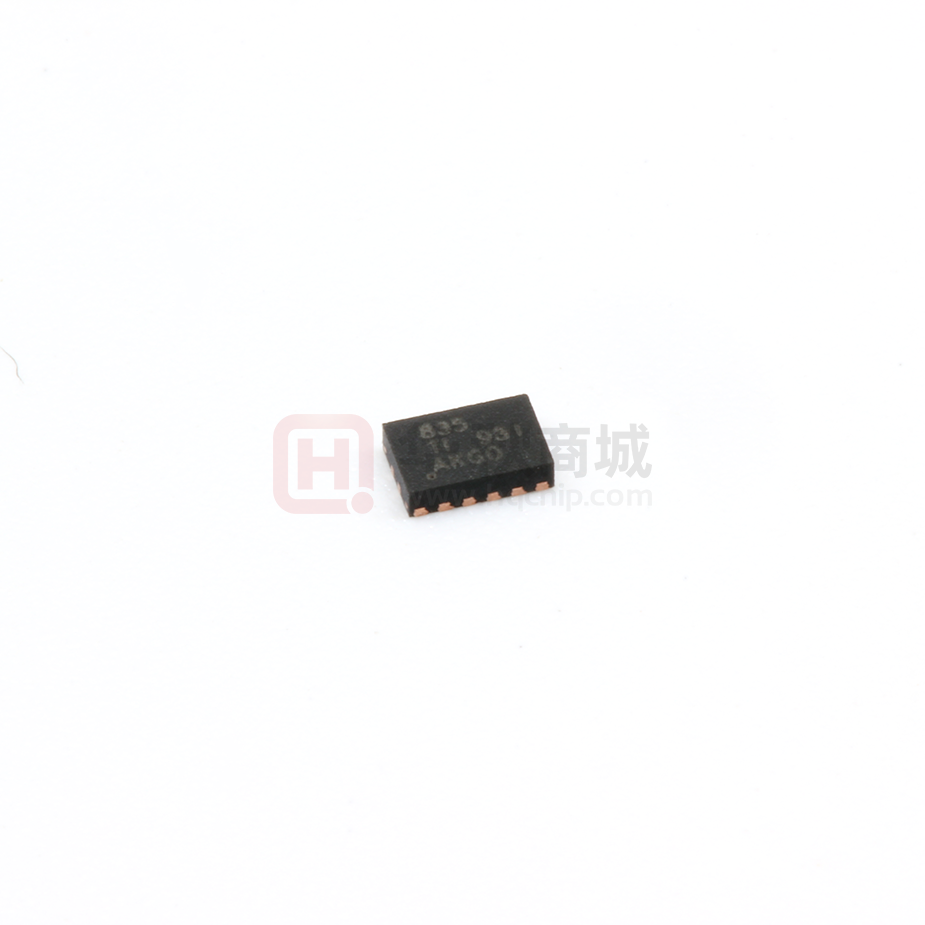
835
(1)
The marketing status values are defined as follows:
ACTIVE: Product device recommended for new designs.
LIFEBUY: TI has announced that the device will be discontinued, and a lifetime-buy period is in effect.
NRND: Not recommended for new designs. Device is in production to support existing customers, but TI does not recommend using this part in a new design.
PREVIEW: Device has been announced but is not in production. Samples may or may not be available.
OBSOLETE: TI has discontinued the production of the device.
(2)
RoHS: TI defines "RoHS" to mean semiconductor products that are compliant with the current EU RoHS requirements for all 10 RoHS substances, including the requirement that RoHS substance
do not exceed 0.1% by weight in homogeneous materials. Where designed to be soldered at high temperatures, "RoHS" products are suitable for use in specified lead-free processes. TI may
reference these types of products as "Pb-Free".
RoHS Exempt: TI defines "RoHS Exempt" to mean products that contain lead but are compliant with EU RoHS pursuant to a specific EU RoHS exemption.
Green: TI defines "Green" to mean the content of Chlorine (Cl) and Bromine (Br) based flame retardants meet JS709B low halogen requirements of