User's Guide
SNOU106 – JUNE 2013
LM3263 DSBGA Evaluation Module
1
Introduction
The LM3263 Evaluation Module is a working demonstration of a step-down DC-DC converter optimized for
powering multimode 2G/3G/4G RF power amplifiers (PAs) from a single Lithium-Ion cell.
The LM3263 steps down an input voltage from 2.7V to 5.5V to a dynamically adjustable output voltage of
0.4V to 3.6V. The output voltage is externally programmed through the RFFE Digital Control Interface and
is set to ensure efficient operation at all power levels of the RF PA.
This application note contains information about the evaluation module. For more details and electrical
characteristics, please refer to the LM3263 datasheet (SNVS837).
2
Operating Conditions
The device will operate under the following conditions:
• VIN range: 2.7V to 5.5V
• VOUT Range: 0.4V to 3.6V
• IOUT range: 0mA to 2.5A
3
Package
The LM3263 is available in a 16-bump (0.4 mm pitch) lead-free DSBGA package.
4
Typical Application Circuit
VBATT
2.7V to 5.5V
0.1 µF
10 µF
PVIN
PACB
SVDD
FB
ACB
Output Voltage
0.4V to 3.6V
1.5 µH
LM3263
SW
10 µF
3.3 nF
GPO1
2G
VCC_PA
BGND
SGND
VIO
SCLK
SDATA
4.7 µF
PA
PGND
3 x 1.0 µF
3G/4G
VCC_PA
PA(s)
1.8V
RFFE
Master
All trademarks are the property of their respective owners.
SNOU106 – JUNE 2013
Submit Documentation Feedback
LM3263 DSBGA Evaluation Module
Copyright © 2013, Texas Instruments Incorporated
1
�Bill of Materials
5
6
www.ti.com
Bill of Materials
Designator
Model
Description
Manufacturer
U1
LM3263TM
DC-DC converter
Texas Instruments
C2
T495D107K010A
100 µF, 10V, 3216 (7343) Low ESR Tantrum Cap
Kemet
C4
CL05A106MP5NUNB
10 µF, 10V, 0402 (1005) Input Bulk capacitor
Samsung
C5
CL05A106MP5NUNB
10 µF, 10V, 0402 (1005) Output Bulk capacitor
Samsung
C7
CL05A475MP5NRNB
4.7 µF, 10V, 0402 (1005) Resemble VCC PA
decoupling capacitor
Samsung
C8, C10, C12
C0603X5R0J105M
1.0 µF, 6.3V, 0201 (0603) Resemble VCC PA
decoupling capacitor
TDK
L1
DFE201610C-1R5N
1.5uH, 2.0 x 1.6 x 1.0 mm, Inductor
Toko
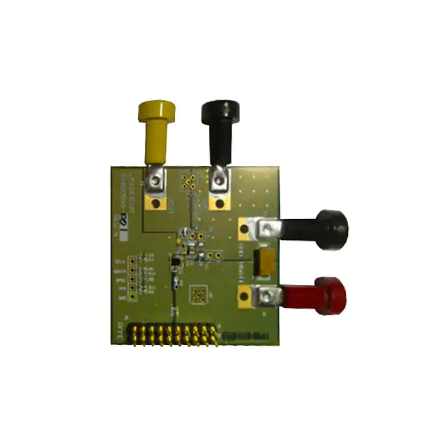
Evaluation Module Photo
20 pin Connector (VIO, SCLK, SDATA,
GND connect to LM8335EVM.)
2
LM3263 DSBGA Evaluation Module
SNOU106 – JUNE 2013
Submit Documentation Feedback
Copyright © 2013, Texas Instruments Incorporated
�Evaluation Module Schematic
www.ti.com
7
Evaluation Module Schematic
Note: R4, R5, R6, R9, R10, R11, R12 are internal use only.
SNOU106 – JUNE 2013
Submit Documentation Feedback
LM3263 DSBGA Evaluation Module
Copyright © 2013, Texas Instruments Incorporated
3
�Connecting to the Module
8
www.ti.com
Connecting to the Module
1.
2.
3.
4.
Connect VBATT to the RED (+) and BLACK (GND) banana connector pins.
Connect the load (resistor or PA) to the YELLOW (+) and BLACK (GND) banana connector pins.
Connect PC USB Power to the LM8335EVM using a micro-USB Type “B” cable.
Connect the RFFE interface ribbon cable from LM8335EVM to the LM3263 Evaluation Module "20-pin
Connector" and align VIO, SDATA, SCLK, and GND.
5. Refer to the Section 11 for information on turning on VIO and other RFFE related questions.
8.1
4
Module Layers
Figure 1. Top Layer
Figure 2. Mid Layer 1
Figure 3. Mid Layer 2
Figure 4. Bottom Layer
LM3263 DSBGA Evaluation Module
SNOU106 – JUNE 2013
Submit Documentation Feedback
Copyright © 2013, Texas Instruments Incorporated
�Connection Diagram
www.ti.com
9
Connection Diagram
PVIN
SW
PGND
ACB
A
A
ACB
PGND
SW
PVIN
PVIN
SW
BGND
PACB
B
B
PACB
BGND
SW
PVIN
VIO
SDATA
FB
ACB
C
C
ACB
FB
SDATA
VIO
SCLK
GPO1
SGND
SVDD
D
D
SVDD
SGND
GPO1
SCLK
1
2
3
4
4
3
2
1
Bottom View
Top View
Figure 5. Connection Diagram
10
Pin Descriptions
Pin #
A1
B1
PVIN
Description
Power Supply Voltage Input to the internal PFET switch.
C1
VIO
VIO functions as the RFFE interface reference voltage. VIO also functions as reset and enable input to the
LM3263. Typically connected to voltage regulator controlled by RF or Baseband IC.
D1
SCLK
Digital control interface RFFE Bus clock input. Typically connected to RFFE master on RF or Baseband IC.
SCLK must be held low when VIO is not applied.
A2
B2
SW
Switching Node connection to the internal PFET switch and NFET synchronous rectifier.
SDATA
Digital control interface RFFE Bus data input/output. Typically connected to RFFE master on RF or
Baseband IC. SDATA must be held low when VIO is not applied.
D2
GPO1
General Purpose Output. Also used to reconfigure USID.
A3
PGND
Power Ground to the internal NFET switch.
B3
BGND
ACB, Analog Bypass Ground and Digital Ground.
C3
FB
D3
SGND
C2
A4
C4
11
Name
ACB
Feedback Analog Input. Connect to the output at the output filter capacitor.
Signal Analog Ground (Low Current).
ACB and Analog Bypass output. Connect to the output at the output filter capacitor.
B4
PACB
ACB Power Supply Input.
D4
SVDD
Analog Power Supply Voltage.
Appendix: LM3263 GUI Software User Guide
11.1 Introduction
The LM3263 software interface facilitates RFFE serial communication between a PC and the LM3263 via
the LM8335 evaluation module (EVM). This version of the software is provided for initial evaluation of the
LM3263.
SNOU106 – JUNE 2013
Submit Documentation Feedback
LM3263 DSBGA Evaluation Module
Copyright © 2013, Texas Instruments Incorporated
5
�Appendix: LM3263 GUI Software User Guide
www.ti.com
11.2 General Information
“The RF Front-End Control Interface (later referred to as RFFE) was developed to offer a common and
widespread method for controlling RF front-end devices. There are a variety of front-end devices, including
Power Amplifiers (PA), Low-Noise Amplifiers (LNA), filters, switches, power management modules,
antenna tuners and sensors. These functions may be located either in separate devices or integrated into
a single device, depending on the application.” -MIPI® Alliance Specification for RFFE
11.3 Items Needed
1.
2.
3.
4.
LM3263 Evaluation Module;
LM8335 Evaluation Module (EVM, including Micro USB "B" cable - order from www.ti.com);
LM3263EVM-to-LM8335EVM Ribbon Cable; and
LM3263 GUI program (download from www.ti.com ).
11.4 Software Installation
NOTE: 1. Version 4.0 or later Microsoft .NET Framework software is required and must be
downloaded from Microsoft.
2. 2010 (32-bit standard RTE) or later version of NI LabVIEW Run-Time Engine is required
and must be downloaded from the Texas Instruments website.
1.
2.
3.
4.
5.
Execute setup.exe onto a computer.
“TI\LM3263 RFFE Interface” directory will be created under C:\Program Files. Click “Next”.
Click the radio button “I accept the License Agreement”, and click “Next”.
Then click “Next”.
Then click “Finish”. Installation Completed.
11.5 Startup Sequence
Ribbon cable connector from
LM3263EVM to LM8335EVM;
Connector showing the following
PINS:
- GND (Pin #1, Pin #8)
- SCLK (Pin #7)
- SDATA (Pin #9
- VIO (Pin #11)
Micro USB-B
connector
Figure 6. LM8335EVM
1. Connect the USB interface board (LM8335EVM) to a PC using the USB cable. VDDIO jumper is
connected VDDIO to 1.8V. Two LEDs (D2, D3) turn on.
2. Connect the LM3263 evaluation module to the LM8335EVM using the provided ribbon cable.
6
LM3263 DSBGA Evaluation Module
SNOU106 – JUNE 2013
Submit Documentation Feedback
Copyright © 2013, Texas Instruments Incorporated
�www.ti.com
Appendix: LM3263 GUI Software User Guide
3. Run the “LM3263 RFFE Interface” in the Start/All Programs menu. All radio buttons are grayed out
except “VIO CONTROL”.
Figure 7. LM3263 GUI Initial Screen
4. Apply power supply voltage to the LM3263 VBATT within the input voltage range of 2.7V to 5.5V.
5. Click “VIO ON”. “VIO STATUS” turns to “VIO ON” in green. And all control boxes and radio buttons are
enabled.
6. The default "TRIGGER MODE" in this GUI is "Non-Triggered" to make evaluation simpler, as opposed
to the device default mode, which is "Triggered".
7. To set the expected output voltage, click the up/down arrow or type in the desired output voltage at the
control box of the “VSET (V)”.
SNOU106 – JUNE 2013
Submit Documentation Feedback
LM3263 DSBGA Evaluation Module
Copyright © 2013, Texas Instruments Incorporated
7
�Appendix: LM3263 GUI Software User Guide
VSET (V)
Control Box for program VOUT
VSET (V)
www.ti.com
Output State (30mV Steps)
Indicator
Output State (15mV Steps)
Figure 8. Programming Output Voltage Windows
NOTE: The other controls in the GUI are dependent on the register map as seen in Section 12.
8
LM3263 DSBGA Evaluation Module
SNOU106 – JUNE 2013
Submit Documentation Feedback
Copyright © 2013, Texas Instruments Incorporated
�Programmable Registers
www.ti.com
12
Programmable Registers
Addr
Register Contents
00h
REGISTER _0
Bits
Function
Default
7
RSVD
0
6:0
VSET[7:1]
00h
Trigger
(1)
N/A
Yes
01h
Description
N/A
Reserved
R/W
Register 00h interacts with Register 03h.
DC-DC converter mode and output voltage control bits
00h : Low-Power Mode
01h : Reserved
02h : Standby Mode
03h to 7Eh : Active Mode, Setting Output Voltage is
enabled. Output voltage can be set 0.4V to 3.6V by
0Dh to 78h with 30 mV steps
7Fh : Forced-Bypass Mode.
VSET[7:1] (dec) = Desired VOUT / 0.03 (round up
decimals), then converts a decimal number to
hexadecimal.
SMPS_CFG
Trigger
(1)
Bits
Function
Default
7:6
RSVD
0
N/A
N/A
Reserved
5
MODE
0
Yes
R/W
Switching mode select bit
0: Forced-PWM Mode (PWM only)
1: Auto-PFM Mode (PFM/PWM)
4
BYPS
0
Yes
R/W
Forced bypass bit
0: Auto-Bypass Mode
1: Forced-Bypass Mode
3:0
RSVD
0h
N/A
N/A
Reserved
02h
R/W
Description
GPO_CTRL
Bits
Function
Default
Trigger (1)
R/W
7
GPO1_OUT
0
Yes
R/W
GPO1 output control
0: Low state
1: High state
6
GPO1_MODE
0
Yes
R/W
GPO1 Mode Selection
0 : General Purpose Output disabled
1 : General Purpose output driven by GPO1_OUT.
5:0
RSVD
00h
N/A
N/A
Reserved
Bits
Function
Default
Trigger (1)
03h
Description
VSET_CTRL
7:0
(1)
R/W
VSET[7:0]
00h
Yes
R/W
Description
R/W
DC-DC converter mode and output voltage fine control
bits
00h-01h : Low-Power Mode
02h-03h : Reserved
04h-05h : Standby Mode
06h to FDh : Active Mode, Setting Output Voltage is
enabled. Output voltage can be set 0.4V to 3.6V by
1Bh to F0h with 15 mV steps
FEh-FFh : Forced Bypass Mode.
VSET[7:0] (dec) = Desired VOUT / 0.015 (round up
decimals), then converts a decimal number to
hexadecimal.
Trigger=Yes: When all PM_TRIG.TRIG_MSK_* bits are set '1', REGISTER_0 will be written immediately during a write
operation. If any PM_TRIG.TRIG_MSK_* bits are cleared ('0'), REGISTER_0 will not be updated to the new value after a write
operation only after an unmasked PM_TRIG.TRIG_* bit is subsequently written to a '1'.
SNOU106 – JUNE 2013
Submit Documentation Feedback
LM3263 DSBGA Evaluation Module
Copyright © 2013, Texas Instruments Incorporated
9
�Programmable Registers
www.ti.com
Addr
Register Contents
1Ah
RFFE_STATUS
Bits
Function
Default
Trigger (2)
7
SWRESET
0
No
6
CMD_FRAME_PERR
0
No
Set if parity error detected in command frame. Cleared
on read. Write will have no effect on this bit.
5
CMD_LENGTH_ERR
0
No
Error when transaction interrupted by new SSC.
Cleared on read. Write will have no effect on this bit.
4
RSVD
0
No
Reserved
3
DATA_FRAME_PER
R
0
No
Write data frame parity error. Cleared on read. Write
will have no effect on this bit.
2
RD_UNUSED_REG
0
No
Read command to an invalid register. Cleared on
read. Write will have no effect on this bit.
1
WR_UNUSED_REG
0
No
Write command to an invalid register. Cleared on
read. Write will have no effect on this bit.
0
BID_GID_ERR
0
No
Read command with a broadcast ID or Group ID.
Cleared on read. Write will have no effect on this bit.
GROUP_ID
Bits
Function
Default
7:4
RSVD
0h
Trigger
N/A
3:0
GSID
0h
No
(2)
1Ch
R/W
N/A
Description
Reserved
Group Slave ID.
PM_TRIG
Bits
10
Description
Software Reset. A write to '1' will cause all registers
except for USID to be reset. Will always read back '0'.
1Bh
(2)
R/W
Function
Default
Trigger (2)
R/W
R/W
Description
Power Mode Bits.
00b = Active Mode
01b = Restore default settings
10b = Low-Power Mode
11b = Reserved
7:6
PWR_MODE
10b
No
5
TRIG_MSK_2
0
No
Mask bit for Trigger 2. Broadcast write to this bit is
ignored.
4
TRIG_MSK_1
0
No
Mask bit for Trigger 1. Broadcast write to this bit is
ignored.
3
TRIG_MSK_0
0
No
Mask bit for Trigger 0. Broadcast write to this bit is
ignored.
2
TRIG_2
0
No
Write to a '1' loads trigger registers with last written
value TRIG_MSK_2 is cleared. Write to '0' has no
affect.
1
TRIG_1
0
No
Write to a '1' loads trigger registers with last written
value TRIG_MSK_1 is cleared. Write to '0' has no
effect.
0
TRIG_0
0
No
Write to a '1' loads trigger registers with last written
value TRIG_MSK_0 is cleared. Write to '0' has no
effect.
Trigger=Yes: When all PM_TRIG.TRIG_MSK_* bits are set '1', REGISTER_0 will be written immediately during a write
operation. If any PM_TRIG.TRIG_MSK_* bits are cleared ('0'), REGISTER_0 will not be updated to the new value after a write
operation only after an unmasked PM_TRIG.TRIG_* bit is subsequently written to a '1'.
LM3263 DSBGA Evaluation Module
SNOU106 – JUNE 2013
Submit Documentation Feedback
Copyright © 2013, Texas Instruments Incorporated
�Programmable Registers
www.ti.com
Addr
Register Contents
1Dh
PRODUCT ID
Bits
Function
Default
7:0
PRODUCT_ID
82h
No
Bits
Function
Default
Trigger (3)
1Eh
R/W
R
Description
Product Identification Bits. Product ID default value
cannot be overwritten.
MANUFACTURER ID, LSB
R/W
7:0
MANID[7:0]
02h
No
Bits
Function
Default
Trigger (3)
R/W
7:6
RSVD
00b
N/A
N/A
5:4
MANID[5:4]
01b
No
R
1Fh
R
Description
Manufacturer Identification, bits 7:0. Manufacturer ID
default value cannot be overwritten.
MANUFACTURER ID, MSB
3:0
(3)
Trigger (3)
USID
010xb
No
Description
Reserved
Manufacturer Identification, bits 5:4. Manufacturer ID
default value cannot be overwritten.
Unique Slave Identifier. Bit 0 (x) of USID is tied to the
state of the GPO1 pin.
0100b: GPO1= Low state or floating
0101b: GPO1= High state
Trigger=Yes: When all PM_TRIG.TRIG_MSK_* bits are set '1', REGISTER_0 will be written immediately during a write
operation. If any PM_TRIG.TRIG_MSK_* bits are cleared ('0'), REGISTER_0 will not be updated to the new value after a write
operation only after an unmasked PM_TRIG.TRIG_* bit is subsequently written to a '1'.
SNOU106 – JUNE 2013
Submit Documentation Feedback
LM3263 DSBGA Evaluation Module
Copyright © 2013, Texas Instruments Incorporated
11
�IMPORTANT NOTICE
Texas Instruments Incorporated and its subsidiaries (TI) reserve the right to make corrections, enhancements, improvements and other
changes to its semiconductor products and services per JESD46, latest issue, and to discontinue any product or service per JESD48, latest
issue. Buyers should obtain the latest relevant information before placing orders and should verify that such information is current and
complete. All semiconductor products (also referred to herein as “components”) are sold subject to TI’s terms and conditions of sale
supplied at the time of order acknowledgment.
TI warrants performance of its components to the specifications applicable at the time of sale, in accordance with the warranty in TI’s terms
and conditions of sale of semiconductor products. Testing and other quality control techniques are used to the extent TI deems necessary
to support this warranty. Except where mandated by applicable law, testing of all parameters of each component is not necessarily
performed.
TI assumes no liability for applications assistance or the design of Buyers’ products. Buyers are responsible for their products and
applications using TI components. To minimize the risks associated with Buyers’ products and applications, Buyers should provide
adequate design and operating safeguards.
TI does not warrant or represent that any license, either express or implied, is granted under any patent right, copyright, mask work right, or
other intellectual property right relating to any combination, machine, or process in which TI components or services are used. Information
published by TI regarding third-party products or services does not constitute a license to use such products or services or a warranty or
endorsement thereof. Use of such information may require a license from a third party under the patents or other intellectual property of the
third party, or a license from TI under the patents or other intellectual property of TI.
Reproduction of significant portions of TI information in TI data books or data sheets is permissible only if reproduction is without alteration
and is accompanied by all associated warranties, conditions, limitations, and notices. TI is not responsible or liable for such altered
documentation. Information of third parties may be subject to additional restrictions.
Resale of TI components or services with statements different from or beyond the parameters stated by TI for that component or service
voids all express and any implied warranties for the associated TI component or service and is an unfair and deceptive business practice.
TI is not responsible or liable for any such statements.
Buyer acknowledges and agrees that it is solely responsible for compliance with all legal, regulatory and safety-related requirements
concerning its products, and any use of TI components in its applications, notwithstanding any applications-related information or support
that may be provided by TI. Buyer represents and agrees that it has all the necessary expertise to create and implement safeguards which
anticipate dangerous consequences of failures, monitor failures and their consequences, lessen the likelihood of failures that might cause
harm and take appropriate remedial actions. Buyer will fully indemnify TI and its representatives against any damages arising out of the use
of any TI components in safety-critical applications.
In some cases, TI components may be promoted specifically to facilitate safety-related applications. With such components, TI’s goal is to
help enable customers to design and create their own end-product solutions that meet applicable functional safety standards and
requirements. Nonetheless, such components are subject to these terms.
No TI components are authorized for use in FDA Class III (or similar life-critical medical equipment) unless authorized officers of the parties
have executed a special agreement specifically governing such use.
Only those TI components which TI has specifically designated as military grade or “enhanced plastic” are designed and intended for use in
military/aerospace applications or environments. Buyer acknowledges and agrees that any military or aerospace use of TI components
which have not been so designated is solely at the Buyer's risk, and that Buyer is solely responsible for compliance with all legal and
regulatory requirements in connection with such use.
TI has specifically designated certain components as meeting ISO/TS16949 requirements, mainly for automotive use. In any case of use of
non-designated products, TI will not be responsible for any failure to meet ISO/TS16949.
Products
Applications
Audio
www.ti.com/audio
Automotive and Transportation
www.ti.com/automotive
Amplifiers
amplifier.ti.com
Communications and Telecom
www.ti.com/communications
Data Converters
dataconverter.ti.com
Computers and Peripherals
www.ti.com/computers
DLP® Products
www.dlp.com
Consumer Electronics
www.ti.com/consumer-apps
DSP
dsp.ti.com
Energy and Lighting
www.ti.com/energy
Clocks and Timers
www.ti.com/clocks
Industrial
www.ti.com/industrial
Interface
interface.ti.com
Medical
www.ti.com/medical
Logic
logic.ti.com
Security
www.ti.com/security
Power Mgmt
power.ti.com
Space, Avionics and Defense
www.ti.com/space-avionics-defense
Microcontrollers
microcontroller.ti.com
Video and Imaging
www.ti.com/video
RFID
www.ti-rfid.com
OMAP Applications Processors
www.ti.com/omap
TI E2E Community
e2e.ti.com
Wireless Connectivity
www.ti.com/wirelessconnectivity
Mailing Address: Texas Instruments, Post Office Box 655303, Dallas, Texas 75265
Copyright © 2013, Texas Instruments Incorporated
�