�������
�� ��
�����
�
� � ��� ������� ���
PCM3002
PCM3003
SBAS079A – OCTOBER 2000 – REVISED OCTOBER 2004
16/20-BIT SINGLE-ENDED ANALOG INPUT/OUTPUT STEREO AUDIO CODECS
FEATURES
•
•
•
•
•
•
•
•
•
Monolithic 20-Bit ∆Σ ADC and DAC
16/20-Bit Input/Output Data
Software Control: PCM3002
Hardware Control: PCM3003
Stereo ADC:
– Single-Ended Voltage Input
– Antialiasing Filter
– 64× Oversampling
– High Performance
• THD+N: –86 dB
• SNR: 90 dB
• Dynamic Range: 90 dB
Stereo DAC:
– Single-Ended Voltage Output
– Analog Low-Pass Filter
– 64× Oversampling
– High Performance
• THD+N: –86 dB
• SNR: 94 dB
• Dynamic Range: 94 dB
Special Features (PCM3002, PCM3003)
– Digital De-Emphasis: 32 kHz, 44.1 kHz,
48 kHz
– Power Down: ADC/DAC Independent
Special Features (PCM3002)
– Digital Attenuation (256 Steps)
– Soft Mute
– Digital Loopback
– Four Alternative Audio Data Formats
Sampling Rate: 4 kHz to 48 kHz
Lch In
Analog Front-End
Rch In
Delta-Sigma
Modulator
•
•
Single 3-V Power Supply
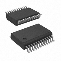
Small Package: SSOP-24
APPLICATIONS
•
•
•
DVC Applications
DSC Applications
Portable/Mobile Audio Applications
DESCRIPTION
The PCM3002 and PCM3003 are low-cost,
single-chip stereo audio codecs (analog-to-digital and
digital-to-analog converters) with single-ended analog
voltage input and output.
The ADCs and DACs employ delta-sigma modulation
with 64-times oversampling. The ADCs include a
digital decimation filter, and the DACs include an
8-times oversampling digital interpolation filter. The
DACs also include digital attenuation, de-emphasis,
infinite zero detection, and soft mute to form a
complete subsystem. The PCM3002 and PCM3003
operate with left-justified (ADC) and right-justified
(DAC) formats, while the PCM3002 also supports
other formats, including the I2S data format.
The PCM3002 and PCM3003 provide a power-down
mode that operates on the ADCs and DACs independently.
The PCM3002 and PCM3003 are fabricated using a
highly advanced CMOS process, and are available in
a 24-pin SSOP package. The PCM3002 and
PCM3003 are suitable for a wide variety of
cost-sensitive consumer applications where good performance is required.
The PCM3002 programmable functions are controlled
by software. The PCM3003 functions, which are
controlled by hardware, include de-emphasis,
power-down, and audio data format selections.
Digital
Decimation
Filter
Digital Out
*
Lch Out
Rch Out
Low-Pass Filter
and
Output Buffer
* PCM3002 Only
Multilevel
Delta-Sigma
Modulator
Digital
Interpolation
Filter
Serial Interface
and
Mode Control
Digital In
Mode Control
System Clock
B0006-01
Please be aware that an important notice concerning availability, standard warranty, and use in critical applications of Texas
Instruments semiconductor products and disclaimers thereto appears at the end of this data sheet.
System Two, Audio Precision are trademarks of Audio Precision, Inc.
All other trademarks are the property of their respective owners.
PRODUCTION DATA information is current as of publication date.
Products conform to specifications per the terms of the Texas
Instruments standard warranty. Production processing does not
necessarily include testing of all parameters.
Copyright © 2000–2004, Texas Instruments Incorporated
�PCM3002
PCM3003
www.ti.com
SBAS079A – OCTOBER 2000 – REVISED OCTOBER 2004
This integrated circuit can be damaged by ESD. Texas Instruments recommends that all integrated
circuits be handled with appropriate precautions. Failure to observe proper handling and installation
procedures can cause damage.
ESD damage can range from subtle performance degradation to complete device failure. Precision
integrated circuits may be more susceptible to damage because very small parametric changes could
cause the device not to meet its published specifications.
ELECTRICAL CHARACTERISTICS
All specifications at TA = 25°C, VDD = VCC = 3 V, fS = 44.1 kHz, SYSCLK = 384 fS, and 16-bit data, unless otherwise noted
PARAMETER
CONDITIONS
PCM3002E/3003E
MIN
TYP
MAX
UNITS
DIGITAL INPUT/OUTPUT
Input Logic
VIH (1) (2) (3)
VIL (1) (2) (3)
IIN (2)
IIN (1) (3)
0.7 VDD
Input logic level
0.3 VDD
±1
Input logic current
100
VDC
µA
Output Logic
VOH (4)
VOL
(4)
IOUT = –1 mA
Output logic level
VOL (5)
VDD – 0.3
IOUT = 1 mA
0.3
IOUT = 1 mA
0.3
VDC
CLOCK FREQUENCY
fs
4 (6)
44.1
48
256 fS
1.024
11.2896
12.288
384 fS
1.536
16.9344
18.432
512 fS
2.048
22.5792
24.576
Sampling frequency
System clock frequency
kHz
MHz
ADC CHARACTERISTICS
Resolution
20
Bits
DC Accuracy
Gain mismatch, channelto-channel
±1
±3
% of FSR
Gain error
±2
±5
% of FSR
±20
Gain drift
ppm of FSR/°C
Bipolar zero error
High-pass filter bypassed (7)
±1.7
% of FSR
Bipolar zero drift
High-pass filter bypassed (7)
±20
ppm of FSR/°C
VIN = –0.5 dB
–86
VIN = –60 dB
–28
Dynamic Performance (8)
THD+N
(2)
(3)
(4)
(5)
(6)
(7)
(8)
2
dB
Dynamic range
A-weighted
86
90
dB
Signal-to-noise ratio
A-weighted
86
90
dB
84
88
dB
Channel separation
(1)
–80
Pins 7, 8, 17 and 18: RST, ML, MD, and MC for the PCM3002; PDAD, PDDA, DEM1, and DEM0 for PCM3003 (Schmitt-trigger input
with 100-kΩ typical internal pulldown resistor)
Pins 9, 10, 11, 15: SYSCLK, LRCIN, BCKIN, DIN (Schmitt-trigger input)
Pin 16: 20BIT for PCM3003 (Schmitt-trigger input, 100-kΩ typical internal pulldown resistor)
Pin 12: DOUT
Pin 16: ZFLG for PCM3002 (open-drain output)
See Application Bulletin SBAA033 for information relating to operation at lower sampling frequencies.
High-pass filter for offset cancel
fIN = 1 kHz, using the System Two™ audio measurement system by Audio Precision™ in rms mode with 20-kHz LPF, 400-Hz HPF used
for performance calculation.
�PCM3002
PCM3003
www.ti.com
SBAS079A – OCTOBER 2000 – REVISED OCTOBER 2004
ELECTRICAL CHARACTERISTICS (continued)
All specifications at TA = 25°C, VDD = VCC = 3 V, fS = 44.1 kHz, SYSCLK = 384 fS, and 16-bit data, unless otherwise noted
PARAMETER
CONDITIONS
PCM3002E/3003E
MIN
TYP
MAX
UNITS
0.454 fS
Hz
Digital Filter Performance
Pass band
Stop band
0.583 fS
Hz
±0.05
Pass-band ripple
Stop-band attenuation
–65
Delay time
dB
dB
17.4/fS
s
0.019 fS
mHz
Voltage range
0.6 VCC
Vp-p
Center voltage
0.5 VCC
VDC
HPF frequency response
–3 dB
Analog Input
Input impedance
Antialiasing filter frequency
response
–3 dB
30
kΩ
150
kHz
20
Bits
DAC CHARACTERISTICS
Resolution
DC Accuracy
±1
±3
Gain error
±1
±5
Gain drift
±20
Bipolar zero error
±2.5
% of FSR
Bipolar zero drift
±20
ppm of FSR/°C
Gain mismatch, channelto-channel
% of FSR
% of FSR
ppm of FSR/°C
Dynamic Performance (9)
THD+N
VOUT = 0 dB (full scale)
–86
VOUT = –60 dB
–32
–80
dB
Dynamic range
EIAJ, A-weighted
88
94
dB
Signal-to-noise ratio
EIAJ, A-weighted
88
94
dB
86
91
dB
Channel separation
Digital Filter Performance
Pass band
0.445 fS
Stop band
0.555 fS
Hz
±0.17
Pass-band ripple
Stop-band attenuation
–35
Delay time
Hz
dB
dB
11.1/fS
s
Voltage range
0.6 VCC
Vp-p
Center voltage
0.5 VCC
VDC
Analog Output
Load impedance
LPF frequency response
(9)
AC coupling
f = 20 kHz
10
kΩ
–0.16
dB
fOUT = 1 kHz, using the System Two audio measurement system by Audio Precision in rms mode with 20-kHz LPF, 400-Hz HPF used
for performance calculation.
3
�PCM3002
PCM3003
www.ti.com
SBAS079A – OCTOBER 2000 – REVISED OCTOBER 2004
ELECTRICAL CHARACTERISTICS (continued)
All specifications at TA = 25°C, VDD = VCC = 3 V, fS = 44.1 kHz, SYSCLK = 384 fS, and 16-bit data, unless otherwise noted
PARAMETER
CONDITIONS
PCM3002E/3003E
MIN
TYP
MAX
UNITS
–25°C to 85°C
2.7
3
3.6
VDC
0° C to 70°C (10)
2.4
3
3.6
VDC
24
mA
72
mW
POWER SUPPLY REQUIREMENTS
VCC, VDD
Supply voltage
Supply current
Power dissipation
Operation, VCC = VDD = 3 V
18
Power down, VCC = VDD = 3 V
50
Operation, VCC = VDD = 3 V
54
Power down (11), VCC = VDD =
3V
150
µA
µW
TEMPERATURE RANGE
TA
Operation
–25
Tstg
Storage
–55
θJA
Thermal resistance
85
125
°C
°C
°C/W
100
(10) Applies for voltages between 2.4 V and 2.7 V for 0°C to 70°C and 256 fS/512 fS operation (384 fS not available)
(11) SYSCLK, BCKIN, and LRCIN are stopped.
PACKAGE/ORDERING INFORMATION
PRODUCT
PACKAGE
TYPE
PACKAGE
CODE
PACKAGE
MARKING
PCM3002E
24-pin SSOP
DB
PCM3002E
PCM3003E
24-pin SSOP
DB
PCM3003E
ORDERING
NUMBER
TRANSPORT
MEDIA
QUANTITY
PCM3002E
Rails
58
PCM3002E/2K
Tape and reel
2000
PCM3003E
Rails
58
PCM3003E/2K
Tape and reel
2000
ABSOLUTE MAXIMUM RATINGS
Supply voltage VDD, VCC1, VCC2
Supply voltage differences
GND voltage differences
Digital input voltage
Analog input voltage
Power dissipation
Input current (any pins except supplies)
Operating temperature
Storage temperature
Lead temperature, soldering
Package temperature (IR reflow, peak)
4
–0.3 V to 6.5 V
±0.1 V
±0.1 V
–0.3 V to VDD + 0.3 V, < 6.5 V
–0.3 V to VCC1, VCC2 + 0.3 V, < 6.5 V
300 mW
±10 mA
–25°C to 85°C
–55°C to 125°C
260°C, 5 s
235°C
�PCM3002
PCM3003
www.ti.com
SBAS079A – OCTOBER 2000 – REVISED OCTOBER 2004
RECOMMENDED OPERATING CONDITIONS
over operating free-air temperature range
MIN
NOM
MAX
Analog supply voltage, VCC1, VCC2
2.7
3
3.6
Digital supply voltage, VDD
2.7
3
3.6
Analog input voltage, full scale (–0 dB)
VCC = 3 V
1.8
Digital input logic family
V
V
Vp-p
CMOS
System clock
Digital input clock frequency
8.192
24.576
MHz
32
48
kHz
Sampling clock
Analog output load resistance
10
kΩ
Analog output load capacitance
30
Digital output load capacitance
10
Operating free-air temperature, TA
1
2
3
4
5
6
7
8
9
10
11
12
pF
pF
–25
PCM3002
(TOP VIEW)
VCC1
VCC1
VINR
VREF1
VREF2
VINL
RST
ML
SYSCLK
LRCIN
BCKIN
DOUT
UNIT
85
°C
PCM3003
(TOP VIEW)
24
23
22
21
20
19
18
17
16
15
14
13
VCC2
AGND1
AGND2
VCOM
VOUTR
VOUTL
MC
MD
ZFLG
DIN
VDD
DGND
VCC1
VCC1
VINR
VREF1
VREF2
VINL
PDAD
PDDA
SYSCLK
LRCIN
BCKIN
DOUT
1
2
3
4
5
6
7
8
9
10
11
12
24
23
22
21
20
19
18
17
16
15
14
13
VCC2
AGND1
AGND2
VCOM
VOUTR
VOUTL
DEM0
DEM1
20BIT
DIN
VDD
DGND
P0004-02
PIN ASSIGNMENTS—PCM3002
(1)
(2)
NAME
PIN
I/O
AGND1
23
–
ADC analog ground
DESCRIPTION
AGND2
22
–
DAC analog ground
BCKIN
11
I
Bit clock input (1)
DGND
13
–
Digital ground
DIN
15
I
Data input (1)
DOUT
12
O
Data output
LRCIN
10
I
Sample rate clock input (fs) (1)
MC
18
I
Bit clock for mode control (1) (2)
MD
17
I
Serial data for mode control (1) (2)
ML
8
I
Strobe pulse for mode control (1) (2)
RST
7
I
Reset, active LOW (1) (2)
SYSCLK
9
I
System clock input (1)
VCC1
1, 2
–
ADC analog power supply
VCC2
24
–
DAC analog power supply
VCOM
21
–
ADC/DAC common
VDD
14
–
Digital power supply
Schmitt-trigger input
With 100-kΩ typical internal pulldown resistor
5
�PCM3002
PCM3003
www.ti.com
SBAS079A – OCTOBER 2000 – REVISED OCTOBER 2004
PIN ASSIGNMENTS—PCM3002 (continued)
(3)
NAME
PIN
I/O
VINL
6
I
ADC analog input, Lch
DESCRIPTION
VINR
3
I
ADC analog input, Rch
VOUTL
19
O
DAC analog output, Lch
VOUTR
20
O
DAC analog output, Rch
VREF1
4
–
ADC reference 1
VREF2
5
–
ADC reference 2
ZFLG
16
O
Zero flag output, active LOW (3)
Open-drain output
PIN ASSIGNMENTS—PCM3003
(1)
(2)
6
NAME
PIN
I/O
AGND1
23
–
ADC analog ground
DESCRIPTION
AGND2
22
–
DAC analog ground
BCKIN
11
I
Bit clock input (1)
DEM0
18
I
De-emphasis control 0 (1) (2)
DEM1
17
I
De-emphasis control 1 (1) (2)
DGND
13
–
Digital ground
DIN
15
I
Data input (1)
DOUT
12
O
Data output
LRCIN
10
I
Sample rate clock input (fs) (1)
PDAD
7
I
ADC power down, active LOW (1) (2)
PDDA
8
I
DAC power down, active LOW (1) (2)
SYSCLK
9
I
System clock input (1)
VCC1
1, 2
–
ADC analog power supply
VCC2
24
–
DAC analog power supply
VCOM
21
–
ADC/DAC common
VDD
14
–
Digital power supply
VINL
6
I
ADC analog input, Lch
VINR
3
I
ADC analog input, Rch
VOUTL
19
O
DAC analog output, Lch
VOUTR
20
O
DAC analog output, Rch
VREF1
4
–
ADC reference 1
VREF2
5
–
ADC reference 2
20BIT
16
I
20-bit format select(1)(2)
Schmitt-trigger input
With 100-kΩ typical internal pulldown resistor
�PCM3002
PCM3003
www.ti.com
SBAS079A – OCTOBER 2000 – REVISED OCTOBER 2004
TYPICAL PERFORMANCE CURVES
All specifications at TA = 25°C, VCC = VDD = 3 V, fS = 44.1 kHz, fSYSCLK = 384 fS, and fSIGNAL = 1 kHz, unless otherwise noted
ADC SECTION
4
0.006
3
−0.5 dB
0.004
0
25
50
75
THD+N − Total Harm. Dist. + Noise at −0.5 dB − %
90
SNR
86
−25
88
0
25
50
75
TA − Free-Air Temperature − °C
G002
Figure 1.
Figure 2.
THD+N
vs
SUPPLY VOLTAGE
DYNAMIC RANGE and SNR
vs
SUPPLY VOLTAGE
5
−60 dB
0.008
4
0.006
3
0.004
2
−0.5 dB
2.7
3.0
3.3
VCC − Supply Voltage − V
Figure 3.
86
100
G001
0.010
2.4
90
92
88
1
100
TA − Free-Air Temperature − °C
0.002
2.1
Dynamic Range
92
3.6
1
3.9
94
94
92
Dynamic Range − dB
0.002
−25
2
94
92
Dynamic Range
90
90
SNR
88
86
2.1
SNR − Signal-to-Noise Ratio − dB
−60 dB
0.008
94
88
2.4
2.7
3.0
3.3
3.6
VCC − Supply Voltage − V
G003
SNR − Signal-to-Noise Ratio − dB
5
Dynamic Range − dB
0.010
THD+N − Total Harm. Dist. + Noise at −60 dB − %
DYNAMIC RANGE and SNR
vs
TEMPERATURE
THD+N − Total Harm. Dist. + Noise at −60 dB − %
THD+N − Total Harm. Dist. + Noise at −0.5 dB − %
THD+N
vs
TEMPERATURE
86
3.9
G004
Figure 4.
NOTE: All characteristics at supply voltages from 2.4 V to 2.7 V are measured at SYSCLK = 256 fS.
7
�PCM3002
PCM3003
www.ti.com
SBAS079A – OCTOBER 2000 – REVISED OCTOBER 2004
TYPICAL PERFORMANCE CURVES (continued)
All specifications at TA = 25°C, VCC = VDD = 3 V, fS = 44.1 kHz, fSYSCLK = 384 fS, and fSIGNAL = 1 kHz, unless otherwise noted
−60 dB
4
0.008
0.006
3
0.004
2
−0.5 dB
0.002
44.1
94
92
92
Dynamic Range
90
90
SNR
88
88
86
1
32
94
86
32
48
44.1
48
fS − Sampling Frequency − kHz
fS − Sampling Frequency − kHz
SNR − Signal-to-Noise Ratio − dB
5
Dynamic Range − dB
0.010
DYNAMIC RANGE and SNR
vs
SAMPLING FREQUENCY
THD+N − Total Harm. Dist. + Noise at −60 dB − %
THD+N − Total Harm. Dist. + Noise at −0.5 dB − %
THD+N
vs
SAMPLING FREQUENCY
G006
G005
Figure 5.
Figure 6.
THD+N
vs
TEMPERATURE
DYNAMIC RANGE and SNR
vs
TEMPERATURE
−60 dB
0.008
3
0.006
2
FS
0.004
0.002
−25
1
0
25
50
75
TA − Free-Air Temperature − °C
Figure 7.
8
0
100
98
98
96
96
Dynamic Range
94
94
SNR
92
90
−25
92
0
25
50
75
TA − Free-Air Temperature − °C
G007
Figure 8.
SNR − Signal-to-Noise Ratio − dB
4
Dynamic Range − dB
THD+N − Total Harm. Dist. + Noise at FS − %
0.010
THD+N − Total Harm. Dist. + Noise at −60 dB − %
DAC SECTION
90
100
G008
�PCM3002
PCM3003
www.ti.com
SBAS079A – OCTOBER 2000 – REVISED OCTOBER 2004
TYPICAL PERFORMANCE CURVES (continued)
All specifications at TA = 25°C, VCC = VDD = 3 V, fS = 44.1 kHz, fSYSCLK = 384 fS, and fSIGNAL = 1 kHz, unless otherwise noted
4
−60 dB
0.008
3
0.006
2
FS
0.004
1
0.002
2.1
2.4
2.7
3.0
3.3
3.6
98
98
96
96
Dynamic Range
94
94
SNR
92
92
90
2.1
0
3.9
2.4
2.7
3.0
3.3
3.6
90
3.9
VCC − Supply Voltage − V
VCC − Supply Voltage − V
G010
G009
Figure 9.
SNR − Signal-to-Noise Ratio − dB
THD+N − Total Harm. Dist. + Noise at FS − %
0.010
Dynamic Range − dB
DYNAMIC RANGE and SNR
vs
SUPPLY VOLTAGE
THD+N − Total Harm. Dist. + Noise at −60 dB − %
THD+N
vs
SUPPLY VOLTAGE
Figure 10.
NOTE: All characteristics at supply voltages from 2.4 V to 2.7 V are measured at SYSCLK = 256 fS.
3
−60 dB
384 fS
256 fS, 512 fS
0.006
2
384 fS
FS
256 fS, 512 fS
0.004
1
0.002
0
32
44.1
Figure 11.
98
256 fS, 512 fS
96
96
SNR
94
94
Dynamic
Range
384 fS
92
92
90
90
32
48
fS − Sampling Frequency − kHz
98
SNR − Signal-to-Noise Ratio − dB
0.008
4
Dynamic Range − dB
THD+N − Total Harm. Dist. + Noise at FS − %
0.010
DYNAMIC RANGE and SNR
vs
SAMPLING FREQUENCY and SYSTEM CLOCK
THD+N − Total Harm. Dist. + Noise at −60 dB − %
THD+N
vs
SAMPLING FREQUENCY and SYSTEM CLOCK
44.1
48
fS − Sampling Frequency − kHz
G011
G012
Figure 12.
9
�PCM3002
PCM3003
www.ti.com
SBAS079A – OCTOBER 2000 – REVISED OCTOBER 2004
TYPICAL PERFORMANCE CURVES (continued)
All specifications at TA = 25°C, VCC = VDD = 3 V, fS = 44.1 kHz, fSYSCLK = 384 fS, and fSIGNAL = 1 kHz, unless otherwise noted
OUTPUT SPECTRUM
ADCs
OUTPUT SPECTRUM (–60 dB, N = 8192)
0
−20
−20
−40
−40
Amplitude − dB
Amplitude − dB
OUTPUT SPECTRUM (–0.5 dB, N = 8192)
0
−60
−80
−60
−80
−100
−100
−120
−120
−140
−140
0
5
10
15
20
25
0
5
f − Frequency − kHz
10
15
G013
Figure 14.
THD+N
vs
SIGNAL LEVEL
THD+N − Total Harmonic Distortion + Noise − %
100
10
1
0.1
0.01
−84
−72
−60
−48
−36
−24
−12
0
Signal Level − dB
G017
Figure 15.
10
25
G015
Figure 13.
0.001
−96
20
f − Frequency − kHz
�PCM3002
PCM3003
www.ti.com
SBAS079A – OCTOBER 2000 – REVISED OCTOBER 2004
TYPICAL PERFORMANCE CURVES (continued)
All specifications at TA = 25°C, VCC = VDD = 3 V, fS = 44.1 kHz, fSYSCLK = 384 fS, and fSIGNAL = 1 kHz, unless otherwise noted
DACs
OUTPUT SPECTRUM (–60 dB, N = 8192)
−20
−20
−40
−40
Amplitude − dB
0
−60
−80
−60
−80
−100
−100
−120
−120
−140
−140
0
5
10
15
20
25
0
5
f − Frequency − kHz
10
15
20
25
f − Frequency − kHz
G014
G016
Figure 16.
Figure 17.
THD+N
vs
SIGNAL LEVEL
100
THD+N − Total Harmonic Distortion + Noise − %
Amplitude − dB
OUTPUT SPECTRUM (0 dB, N = 8192)
0
10
1
0.1
0.01
0.001
−96
−84
−72
−60
−48
−36
−24
−12
0
Signal Level − dB
G018
Figure 18.
11
�PCM3002
PCM3003
www.ti.com
SBAS079A – OCTOBER 2000 – REVISED OCTOBER 2004
TYPICAL PERFORMANCE CURVES
All specifications at TA = 25°C, VCC = VDD = 3 V, fS = 44.1 kHz, fSYSCLK = 384 fS, DIN = BPZ, and VIN = BPZ, unless otherwise
noted
SUPPLY CURRENT
ICC + IDD
vs
SUPPLY VOLTAGE
ICC + IDD
vs
TEMPERATURE
25
2.0
ICC + IDD − mA
ADC and DAC
15
1.5
ADC
10
1.0
DAC
5
0.5
2.5
20
ICC + IDD − mA
20
ICC + IDD: Power Down and Off − mA
2.5
15
1.5
ADC
10
1.0
DAC
5
0.5
Power Down and Off
0
2.1
2.4
2.7
3.0
3.3
Power Down and Off
3.6
0
−50
0
3.9
VCC − Supply Voltage − V
−25
0
25
Figure 20.
All characteristics at supply voltages from 2.4 V to
2.7 V are measured at SYSCLK = 256 fS.
ICC + IDD
vs
SAMPLING FREQUENCY
20
ADC and DAC
19
512 fS
ICC + IDD − mA
50
TA − Free-Air Temperature − °C
G020
Figure 19.
18
256 fS
17
16
15
32
44.1
48
fS − Sampling Frequency − kHz
Figure 21.
12
2.0
ADC and DAC
ICC + IDD: Power Down and Off − mA
25
G021
75
0
100
G019
�PCM3002
PCM3003
www.ti.com
SBAS079A – OCTOBER 2000 – REVISED OCTOBER 2004
TYPICAL PERFORMANCE CURVES OF INTERNAL FILTERS (ADCs)
All specifications at TA = 25°C, VCC = VDD = 3 V, fS = 44.1 kHz, and fSYSCLK = 384 fS, unless otherwise noted
DECIMATION FILTER
OVERALL CHARACTERISTICS
STOP-BAND ATTENUATION CHARACTERISTICS
0
0
−20
Amplitude − dB
Amplitude − dB
−50
−100
−40
−60
−150
−80
−200
0
8
16
24
Normalized Frequency [× fS Hz]
−100
0.0
32
0.2
0.4
0.6
0.8
Normalized Frequency [× fS Hz]
G022
Figure 22.
1.0
G023
Figure 23.
PASS-BAND RIPPLE CHARACTERISTICS
TRANSITION BAND CHARACTERISTICS
0.2
0
−1
−2
−3
−0.2
Amplitude − dB
Amplitude − dB
0.0
−0.4
−0.6
−4
−5
−6
−7
−8
−0.8
−9
−1.0
0.0
0.1
0.2
0.3
0.4
Normalized Frequency [× fS Hz]
Figure 24.
0.5
G024
−4.13 dB at 0.5 fS
−10
0.45
0.47
0.49
0.51
0.53
Normalized Frequency [× fS Hz]
0.55
G025
Figure 25.
13
�PCM3002
PCM3003
www.ti.com
SBAS079A – OCTOBER 2000 – REVISED OCTOBER 2004
TYPICAL PERFORMANCE CURVES OF INTERNAL FILTERS (ADCs) (continued)
All specifications at TA = 25°C, VCC = VDD = 3 V, fS = 44.1 kHz, and fSYSCLK = 384 fS, unless otherwise noted
HIGH-PASS FILTER
HIGH-PASS FILTER RESPONSE
HIGH-PASS FILTER RESPONSE
0
0.2
−10
0.0
−20
Amplitude − dB
Amplitude − dB
−30
−40
−50
−60
−70
−80
−0.2
−0.4
−0.6
−0.8
−90
−100
0.0
−1.0
0.1
0.2
0.3
0.4
Normalized Frequency [× fS/1000 Hz]
0.5
0
1
2
3
4
Normalized Frequency [× fS/1000 Hz]
G026
Figure 26.
G027
Figure 27.
ANTIALIASING FILTER
ANTIALIASING FILTER OVERALL
FREQUENCY RESPONSE
ANTIALIASING FILTER PASS-BAND
FREQUENCY RESPONSE
0.2
0
0.0
Amplitude − dB
Amplitude − dB
−10
−20
−30
−40
−0.2
−0.4
−0.6
−0.8
−50
−1.0
1
10
100
1k
10k
100k
1M
10M
f − Frequency − Hz
1
10
100
1k
G028
Figure 28.
14
10k
100k
f − Frequency − Hz
G029
Figure 29.
�PCM3002
PCM3003
www.ti.com
SBAS079A – OCTOBER 2000 – REVISED OCTOBER 2004
TYPICAL PERFORMANCE CURVES OF INTERNAL FILTERS (DACs)
All specifications at TA = 25°C, VCC = VDD = 3 V, fS = 44.1 kHz, and fSYSCLK = 384 fS, unless otherwise noted
DIGITAL FILTER
PASS-BAND RIPPLE CHARACTERISTICS
(fS = 44.1 kHz)
0
0.00
−20
−0.20
−40
−0.40
Level − dB
Level − dB
OVERALL FREQUENCY CHARACTERISTICS
(fS = 44.1 kHz)
−60
−80
−0.60
−0.80
−100
−1.00
0
25k
50k
75k
100k
125k
150k
175k
0
5k
f − Frequency − Hz
10k
15k
20k
f − Frequency − Hz
G030
G031
Figure 30.
Figure 31.
DE-EMPHASIS FILTER
DE-EMPHASIS ERROR (32 kHz)
0.6
−2
0.4
−4
0.2
Error − dB
Level − dB
DE-EMPHASIS FREQUENCY RESPONSE (32 kHz)
0
−6
0.0
−8
−0.2
−10
−0.4
−12
−0.6
0
5k
10k
15k
20k
25k
f − Frequency − Hz
0
3628
7256
G032
Figure 32.
10884
14512
f − Frequency − Hz
G033
Figure 33.
15
�PCM3002
PCM3003
www.ti.com
SBAS079A – OCTOBER 2000 – REVISED OCTOBER 2004
TYPICAL PERFORMANCE CURVES OF INTERNAL FILTERS (DACs) (continued)
All specifications at TA = 25°C, VCC = VDD = 3 V, fS = 44.1 kHz, and fSYSCLK = 384 fS, unless otherwise noted
DE-EMPHASIS ERROR (44.1 kHz)
0.6
−2
0.4
−4
0.2
Error − dB
Level − dB
DE-EMPHASIS FREQUENCY RESPONSE (44.1 kHz)
0
−6
0.0
−8
−0.2
−10
−0.4
−12
−0.6
0
5k
10k
15k
20k
25k
0
4999.8375
f − Frequency − Hz
9999.675
14999.5125
G034
G035
Figure 34.
Figure 35.
DE-EMPHASIS ERROR (48 kHz)
0
0.6
−2
0.4
−4
0.2
Error − dB
Level − dB
DE-EMPHASIS FREQUENCY RESPONSE (48 kHz)
−6
0.0
−8
−0.2
−10
−0.4
−12
−0.6
0
5k
10k
15k
20k
25k
f − Frequency − Hz
0
5442
10884
Figure 36.
16326
21768
f − Frequency − Hz
G036
16
19999.35
f − Frequency − Hz
G037
Figure 37.
�PCM3002
PCM3003
www.ti.com
SBAS079A – OCTOBER 2000 – REVISED OCTOBER 2004
TYPICAL PERFORMANCE CURVES OF INTERNAL FILTERS (DACs) (continued)
All specifications at TA = 25°C, VCC = VDD = 3 V, fS = 44.1 kHz, and fSYSCLK = 384 fS, unless otherwise noted
ANALOG LOW-PASS FILTER
INTERNAL ANALOG FILTER FREQUENCY RESPONSE
(1 Hz–100 kHz)
20
0.15
0
0.10
−20
0.05
Level − dB
Level − dB
INTERNAL ANALOG FILTER FREQUENCY RESPONSE
(1 Hz–10 MHz)
−40
0.00
−60
−0.05
−80
−0.10
−100
−0.15
1
10
100
1k
10k
100k
1M
10M
f − Frequency − Hz
1
10
100
1k
G038
Figure 38.
10k
100k
f − Frequency − Hz
G039
Figure 39.
17
�PCM3002
PCM3003
www.ti.com
SBAS079A – OCTOBER 2000 – REVISED OCTOBER 2004
BLOCK DIAGRAM
(+)
VINL
VREF1
VCOM
VREF2
Analog
Front-End
Circuit
(−)
Decimation
and
High-Pass Filter
Delta-Sigma
Modulator
LRCIN
BCKIN
Serial Data
Interface
ADC
Reference
DIN
(−)
VINR
Analog
Front-End
Circuit
VOUTL
Analog
Low-Pass
Filter
(+)
Delta-Sigma
Modulator
Decimation
and
High-Pass Filter
Multilevel
Delta-Sigma
Modulator
Interpolation
Filter
8× Oversampling
DOUT
MC(1)/DEM0(2)
Mode
Control
Interface
DAC
VOUTR
Analog
Low-Pass
Filter
Multilevel
Delta-Sigma
Modulator
MD(1)/DEM1(2)
ML(1)
20BIT(2)
Interpolation
Filter
8× Oversampling
Reset and
Power Down
PDDA(2)
RST(1)/PDAD(2)
Power Supply
AGND2
VCC2
AGND1
VCC1
DGND
VDD
Clock
Zero Detect(1)
SYSCLK
ZFLG(1)
B0004-03
18
(1)
MC, MD, ML, RST, and ZFLG are for PCM3002 only.
(2)
DEM0, DEM1, 20BIT, PDAD, and PDDA are for PCM3003 only.
�PCM3002
PCM3003
www.ti.com
SBAS079A – OCTOBER 2000 – REVISED OCTOBER 2004
1.0 µF
+
3
VINR 30 kΩ
−
−
(+)
+
+
(−)
21
4.7 µF
VCOM
Delta-Sigma
Modulator
+
4
4.7 µF
VREF1
+
5
4.7 µF
VREF2
+
VREF
S0011-03
Figure 40. Analog Front-End (Single-Channel)
PCM AUDIO INTERFACE
The four-wire digital audio interface for the PCM3002/3003 comprises LRCIN (pin 10), BCKIN (pin 11), DIN
(pin 15), and DOUT (pin 12). The PCM3002 can be used with any of the four input/output data formats (formats
0–3), while the PCM3003 can only be used with selected input/output formats (formats 0–1). For the PCM3002,
these formats are selected through program register 3 in the software mode. For the PCM3003, data formats are
selected by the 20BIT input (pin 16). Figure 41, Figure 42, and Figure 43 illustrate audio data input/output
formats and timing.
The PCM3002/3003 can accept 32, 48, or 64 bit clocks (BCKIN) in one clock of LRCIN. Only the 16-bit data
format can be selected when 32-bit clocks/LRCIN are applied.
19
�PCM3002
PCM3003
www.ti.com
SBAS079A – OCTOBER 2000 – REVISED OCTOBER 2004
FORMAT 0: PCM3002/3003
DAC: 16-Bit, MSB-First, Right-Justified
LRCIN
Left-Channel
Right-Channel
BCKIN
DIN
16
1
2
3
14 15 16
MSB
1
2
3
14 15 16
MSB
LSB
LSB
ADC: 16-Bit, MSB-First, Left-Justified
Left-Channel
LRCIN
Right-Channel
BCKIN
DOUT
1
2
3
14 15 16
MSB
1
LSB
2
3
1
14 15 16
MSB
LSB
FORMAT 1: PCM3002/3003
DAC: 20-Bit, MSB-First, Right-Justified
LRCIN
Left-Channel
Right-Channel
BCKIN
DIN
20
1
2
3
18 19 20
MSB
1
2
3
18 19 20
MSB
LSB
LSB
ADC: 20-Bit, MSB-First, Left-Justified
Left-Channel
LRCIN
Right-Channel
BCKIN
DOUT
1
2
MSB
3
18 19 20
LSB
1
2
3
MSB
18 19 20
1
LSB
T0016-04
Figure 41. Audio Data Input/Output Format
20
�PCM3002
PCM3003
www.ti.com
SBAS079A – OCTOBER 2000 – REVISED OCTOBER 2004
FORMAT 2: PCM3002 Only
DAC: 20-Bit, MSB-First, Left-Justified
Left-Channel
LRCIN
Right-Channel
BCKIN
DIN
1
2
3
18 19 20
MSB
1
LSB
2
3
1
18 19 20
MSB
LSB
ADC: 20-Bit, MSB-First, Left-Justified
Left-Channel
LRCIN
Right-Channel
BCKIN
DOUT
1
2
3
18 19 20
MSB
1
LSB
2
3
1
18 19 20
MSB
LSB
FORMAT 3: PCM3002 Only
DAC: 20-Bit, MSB-First, I2S
Left-Channel
LRCIN
Right-Channel
BCKIN
DIN
1
2
3
18 19 20
MSB
LSB
1
2
3
18 19 20
MSB
LSB
ADC: 20-Bit, MSB-First, I2S
Left-Channel
LRCIN
Right-Channel
BCKIN
DOUT
1
2
MSB
3
18 19 20
LSB
1
2
3
MSB
18 19 20
LSB
T0016-05
Figure 42. Audio Data Input/Output Format (PCM3002)
21
�PCM3002
PCM3003
www.ti.com
SBAS079A – OCTOBER 2000 – REVISED OCTOBER 2004
t(LRP)
0.5 VDD
LRCIN
t(BCL)
t(BCH)
t(LB)
t(BL)
0.5 VDD
BCKIN
t(BCY)
t(DIH)
t(DIS)
0.5 VDD
DIN
t(BDO)
t(LDO)
0.5 VDD
DOUT
T0021−01
BCKIN pulse cycle time
t(BCY)
300 ns (min)
BCKIN pulse duration, HIGH
t(BCH)
120 ns (min)
BCKIN pulse duration, LOW
t(BCL)
120 ns (min)
BCKIN rising edge to LRCIN edge
t(BL)
40 ns (min)
LRCIN edge to BCKIN rising edge
t(LB)
40 ns (min)
LRCIN pulse duration
t(LRP)
t(BCY) (min)
DIN setup time
t(DIS)
40 ns (min)
DIN hold time
t(DIH)
40 ns (min)
DOUT delay time to BCKIN falling edge
t(BDO)
40 ns (max)
DOUT delay time to LRCIN edge
t(LDO)
40 ns (max)
Rising time of all signals
t(RISE)
20 ns (max)
Falling time of all signals
t(FALL)
20 ns (max)
Figure 43. Audio Data Input/Output Timing
SYSTEM CLOCK
The system clock for the PCM3002/3003 must be either 256 fS, 384 fS, or 512 fS, where fS is the audio sampling
frequency. The system clock should be provided at the SYSCLK input (pin 9).
The PCM3002/3003 also has a system-clock detection circuit that automatically senses if the system clock is
operating at 256 fS, 384 fS, or 512 fS. When a 384-fS or 512-fS system clock is used, the clock is divided to 256 fS
automatically. The 256-fS clock is used to operate the digital filters and the delta-sigma modulators.
Table 1 lists the relationship of typical sampling frequencies and system clock frequencies; Figure 44 illustrates
the system clock timing.
Table 1. System Clock Frequencies
SAMPLING RATE FREQUENCY (kHz)
22
SYSTEM CLOCK FREQUENCY (MHz)
256 fs
384 fs
512 fs
32
8.1920
12.2880
16.3840
44.1
11.2896
16.9344
22.5792
48
12.2880
18.4320
24.5760
�PCM3002
PCM3003
www.ti.com
SBAS079A – OCTOBER 2000 – REVISED OCTOBER 2004
t(SCKH)
H
0.7 VDD
SYSCLK
0.3 VDD
L
1/256 fS,
1/384 fS,
or 1/512 fS
t(SCKL)
T0005-05
Figure 44. System Clock Timing
System clock pulse duration, HIGH
t(SCKH)
12 ns (min)
System clock pulse duration, LOW
t(SCKL)
12 ns (min)
POWER-ON RESET
Both the PCM3002 and PCM3003 have internal power-on reset circuitry. Power-on reset occurs when the
system clock (SYSCLK) is active and VDD > 2.2 V. For the PCM3003, the SYSCLK must complete a minimum of
three complete cycles prior to VDD > 2.2 V to ensure proper reset operation. The initialization sequence requires
1024 SYSCLK cycles for completion, as shown in Figure 45. Figure 46 shows the state of the DAC and ADC
outputs during and after the reset sequence.
VDD
2.4 V
2.2 V
2.0 V
Reset
Reset Removal
Internal Reset
3 Clocks Minimum
1024 System Clock Periods
System Clock
T0014-03
Figure 45. Internal Power-On Reset Timing
23
�PCM3002
PCM3003
www.ti.com
SBAS079A – OCTOBER 2000 – REVISED OCTOBER 2004
Reset Removal or Power Down Off
Internal Reset
or Power Down
Reset
Ready/Operation
Power Down
t(DACDLY1)
(16384/fS)
DAC VOUT
GND
VCOM
(0.5 VCC)
t(ADCDLY1)
(18432/fS)
ADC DOUT
Zero Data
Zero Data
Normal Data(1)
T0019-02
(1)
The HPF transient response (exponentially attenuated signal from ±0.2% dc of FSR with 200-ms time constant)
appears initially.
Figure 46. DAC Output and ADC Output for Reset and Power Down
EXTERNAL RESET
The PCM3002 includes a reset input, RST (pin 7), while the PCM3003 uses both PDAD (pin 7) and PDDA
(pin 8) for external reset control. As shown in Figure 47, the external reset signal must drive RST or PDAD and
PDDA low for a minimum of 40 nanoseconds while SYSCLK is active in order to initiate the reset sequence.
Initialization starts on the rising edge of RST or PDAD and PDDA, and requires 1024 SYSCLK cycles for
completion. Figure 46 shows the state of the DAC and ADC outputs during and after the reset sequence.
RST
or
PDAD and PDDA
RST Pulse Duration
t(RST) = 40 ns (min)
t(RST)
Reset
Reset Removal
Internal Reset
1024 System Clock Periods
System Clock
T0015-02
Figure 47. External Forced-Reset Timing
SYNCHRONIZATION WITH THE DIGITAL AUDIO SYSTEM
The PCM3002/3003 operates with LRCIN synchronized to the system clock. The PCM3002/3003 does not
require any specific phase relationship between LRCIN and the system clock, but there must be synchronization
of LRCIN and the system clock. If the synchronization between the system clock and LRCIN changes more than
6 bit clocks (BCKIN) during one sample (LRCIN) period because of phase jitter on LRCIN, internal operation of
the DAC stops within 1/fS, and the analog output is forced to bipolar zero (0.5 VCC) until the system clock is
resynchronized to LRCIN followed by t(DACDLY2) delay time. Internal operation of the ADC also stops within 1/fS,
and the digital output codes are set to bipolar zero until resynchronization occurs followed by t(ADCDLY2) delay
time. If LRCIN is synchronized within 5 or fewer bit clocks to the system clock, operation is normal. Figure 48
illustrates the effects on the output when synchronization is lost. Before the outputs are forced to bipolar zero
( 10 kΩ, depending on system performance requirements
(6)
MC, MD, ML, ZFLG, RST, and 10-kΩ pullup resistor are for the PCM3002.
(7)
DEM0, DEM1, 20BIT, PDAD, PDDA are for the PCM3003.
Figure 51. Typical Connection Diagram for PCM3002/3003
33
�PCM3002
PCM3003
www.ti.com
SBAS079A – OCTOBER 2000 – REVISED OCTOBER 2004
THEORY OF OPERATION
ADC SECTION
The PCM3002/3003 ADC consists of two reference circuits, a stereo single-to-differential converter, a fully
differential fifth-order delta-sigma modulator, a decimation filter (including digital high pass), and a serial interface
circuit. The block diagram in this data sheet illustrates the architecture of the ADC section, Figure 40 shows the
single-to-differential converter, and Figure 52 illustrates the architecture of the fifth-order delta-sigma modulator
and transfer functions.
An internal reference circuit with three external capacitors provides all reference voltages required by the ADC,
which defines the full-scale range for the converter. The internal single-to-differential voltage converter saves the
space and extra parts needed for the external circuitry required by many delta-sigma converters. The internal
full-differential signal processing architecture provides a wide dynamic range and excellent power supply
rejection performance. The input signal is sampled at a 64× oversampling rate, eliminating the need for a
sample-and-hold circuit, and simplifying antialias filtering requirements. The fifth-order delta-sigma noise shaper
consists of five integrators which use a switched-capacitor topology, a comparator, and a feedback loop
consisting of a one-bit DAC. The delta-sigma modulator shapes the quantization noise, shifting it out of the audio
band in the frequency domain. The high order of the modulator enables it to randomize the modulator outputs,
reducing idle tone levels.
The 64-fS, one-bit data stream from the modulator is converted to 1-fS, 16/20-bit data words by the decimation
filter, which also acts as a low-pass filter to remove the shaped quantization noise. The dc components are
removed by a high-pass filter function contained within the decimation filter.
DAC SECTION
The delta-sigma DAC section of the PCM3002/3003 is based on a 5-level amplitude quantizer and a third-order
noise shaper. This section converts the oversampled input data to a 5-level delta-sigma format. A block diagram
of the 5-level delta-sigma modulator is shown in Figure 53. This 5-level delta-sigma modulator has the advantage
of improved stability and reduced clock-jitter sensitivity over the typical one-bit (2-level) delta-sigma modulator.
The combined oversampling rate of the delta-sigma modulator and the internal 8× interpolation filter is 64 fS for a
256-fS system clock. The theoretical quantization noise performance of the 5-level delta-sigma modulator is
shown in Figure 54.
Analog
In
X(z) +
−
1st
SW-CAP
Integrator
+
−
2nd
SW-CAP
Integrator
+
3rd
SW-CAP
Integrator
+
+
+
+
−
4th
SW-CAP
Integrator
+
5th
SW-CAP
Integrator
+
H(z)
+
Qn(z)
Digital
Out
Y(z)
+
Comparator
1-Bit
DAC
Y(z) = STF(z) * X(z) + NTF(z) * Qn(z)
Signal Transfer Function
STF(z) = H(z) / [1 + H(z)]
Noise Transfer Function
NTF(z) = 1 / [1 + H(z)]
B0005-01
Figure 52. Simplified Fifth-Order Delta-Sigma Modulator
34
�PCM3002
PCM3003
www.ti.com
SBAS079A – OCTOBER 2000 – REVISED OCTOBER 2004
THEORY OF OPERATION (continued)
In
8 fS
21-Bit
+
+
+
Z−1
−
+
−
+
+
Z−1
+
+
Z−1
+
5-Level Quantizer
4
3
Out
64 fS
2
1
0
B0008-01
Figure 53. Five-Level Delta-Sigma Modulator Block Diagram
0
−10
−20
−30
−40
Gain − dB
−50
−60
−70
−80
−90
−100
−110
−120
−130
−140
−150
0
5
10
15
20
25
30
f − Frequency − kHz
G040
Figure 54. Quantization Noise Spectrum
35
�PACKAGE OPTION ADDENDUM
www.ti.com
17-May-2022
PACKAGING INFORMATION
Orderable Device
Status
(1)
Package Type Package Pins Package
Drawing
Qty
Eco Plan
(2)
Lead finish/
Ball material
MSL Peak Temp
Op Temp (°C)
Device Marking
(3)
Samples
(4/5)
(6)
PCM3002E
ACTIVE
SSOP
DB
24
58
RoHS & Green
NIPDAU
Level-1-260C-UNLIM
-25 to 85
PCM3002E
Samples
PCM3002E/2K
ACTIVE
SSOP
DB
24
2000
RoHS & Green
NIPDAU
Level-1-260C-UNLIM
-25 to 85
PCM3002E
Samples
PCM3003E
ACTIVE
SSOP
DB
24
58
RoHS & Green
NIPDAU
Level-1-260C-UNLIM
PCM3003E
Samples
PCM3003E/2K
ACTIVE
SSOP
DB
24
2000
RoHS & Green
NIPDAU
Level-1-260C-UNLIM
PCM3003E
Samples
(1)
The marketing status values are defined as follows:
ACTIVE: Product device recommended for new designs.
LIFEBUY: TI has announced that the device will be discontinued, and a lifetime-buy period is in effect.
NRND: Not recommended for new designs. Device is in production to support existing customers, but TI does not recommend using this part in a new design.
PREVIEW: Device has been announced but is not in production. Samples may or may not be available.
OBSOLETE: TI has discontinued the production of the device.
(2)
RoHS: TI defines "RoHS" to mean semiconductor products that are compliant with the current EU RoHS requirements for all 10 RoHS substances, including the requirement that RoHS substance
do not exceed 0.1% by weight in homogeneous materials. Where designed to be soldered at high temperatures, "RoHS" products are suitable for use in specified lead-free processes. TI may
reference these types of products as "Pb-Free".
RoHS Exempt: TI defines "RoHS Exempt" to mean products that contain lead but are compliant with EU RoHS pursuant to a specific EU RoHS exemption.
Green: TI defines "Green" to mean the content of Chlorine (Cl) and Bromine (Br) based flame retardants meet JS709B low halogen requirements of


 工商网监
湘ICP备2023018690号
工商网监
湘ICP备2023018690号
