User's Guide
SLLU169 – July 20112
SN65LVCP1414 Evaluation Module (EVM)
The Texas Instruments SN65LVCP1414 Evaluation Module (EVM) board is used to evaluate the
SN65LVCP1414, 14.2-Gbps quad-channel, dual mode linear-redriver with signal conditioning. This
document provides guidance on the devices proper use by showing some operating configurations and
test modes. In addition, the EVM board schematic and layout information are provided. Information in this
guide assists in choosing the optimal design methods and materials for designing a complete system.
Contents
1
Introduction .................................................................................................................. 4
2
EVM PCB and High-Speed Design Considerations .................................................................... 4
3
SN65LVCP1414 EVM Kit Contents ...................................................................................... 4
4
SN65LVCP1414 EVM Board Configuration ............................................................................. 4
5
Test Setup ................................................................................................................... 7
6
I2C Mode ..................................................................................................................... 8
7
GPIO Mode .................................................................................................................. 9
8
Schematics ................................................................................................................. 10
9
Bill of Materials ............................................................................................................. 15
10
Board Layout ............................................................................................................... 16
Appendix A
Jumper Shunt Settings ........................................................................................... 21
List of Figures
.....................................................................................................
1
SN65LVCP1414 EVM
2
USB Dongle Board.......................................................................................................... 6
3
SN65LVCP1414 EVM Jumper Description .............................................................................. 7
4
SN65LVCP1414 EVM Schematic, Sheet 1 Inputs and Outputs
5
SN65LVCP1414 EVM Schematic, Sheet 2 GPIO Controls .......................................................... 11
6
SN65LVCP1414 EVM Schematic, Sheet 3 I2C Controls ............................................................. 12
7
SN65LVCP1414 EVM Schematic, Sheet 4 I2C Communications ................................................... 13
8
SN65LVCP1414 EVM Schematic, Sheet 5 Power .................................................................... 14
9
SN65LVCP1414 Board Layout: Top Signal (Layer 1) ................................................................ 17
10
SN65LVCP1414 Board Layout: Internal Ground (Layer 2) .......................................................... 18
11
SN65LVDS1414 EVM Board Layout: Internal Power (Layer 3) ..................................................... 19
12
SN65LVCP1414 Board Layout: Bottom Signal (Layer 4) ............................................................ 20
....................................................
5
10
List of Tables
1
SN65LVCP1414 EVM Pin and Jumper Functionality Description .................................................... 8
2
SN65LVCP1414 EVM I2C Mode Settings................................................................................ 8
3
SN65LVCP1414 EVM Jumper and EQ Settings ........................................................................ 9
4
SN65LVCP1414 EVM GPIO Mode Settings
5
SN65LVCP1414 EVM Bill of Materials ................................................................................. 15
6
SN65LVCP1414 EVM PCB Layer Construction ....................................................................... 16
............................................................................
9
I2C is a trademark of Philips Semiconductor Corp..
SLLU169 – July 20112
Submit Documentation Feedback
SN65LVCP1414 Evaluation Module (EVM)
Copyright © 20112, Texas Instruments Incorporated
1
�www.ti.com
2
SN65LVCP1414 Evaluation Module (EVM)
Copyright © 20112, Texas Instruments Incorporated
SLLU169 – July 20112
Submit Documentation Feedback
�www.ti.com
WARNING
This equipment is intended for use in a laboratory test environment
only. It generates, uses, and can radiate radio frequency energy
and has not been tested for compliance with the limits of
computing devices pursuant to subpart J of part 15 of FCC rules,
which are designed to provide reasonable protection against radio
frequency interference. Operation of this equipment in other
environments may cause interference with radio communications,
in which case the user, at their own expense, is required to take
whatever measures are required to correct this interference.
SLLU169 – July 20112
Submit Documentation Feedback
SN65LVCP1414 Evaluation Module (EVM)
Copyright © 20112, Texas Instruments Incorporated
3
�Introduction
1
www.ti.com
Introduction
The Texas Instruments (TI) SN65LVCP1414 is a 14.2-Gbps quad channel dual mode linear-redriver with
signal conditioning. The device linearly compensates for channel loss in backplane and active-cable
applications. The architecture of SN65LVCP1414 linear-redriver is designed to work effectively with ASIC
or FPGA products implementing digital equalization using decision feedback equalizer (DFE) technology.
SN65LVCP1414 preserves the integrity (composition) of the received signal ensuring optimum DFE and
system performance. SN65LVCP1414 provides a low power linear-redriver solution while at the same time
extending the effectiveness of DFE.
2
EVM PCB and High-Speed Design Considerations
Use the EVM and the contents of this guide to evaluate device parameters in addition to helping with highspeed board layout. As the frequency of operation increases, special care is required to ensure that the
highest signal integrity is maintained. Achieve this by controlling the board's impedance to 50 Ω singleended or 100-Ω differential. The use of vias is minimized and, when necessary, are designed to minimize
impedance discontinuities along the transmission line. Care was taken to control trace length mismatch
(board skew) to less than ±0.001 in.
Overall, the board layout is designed and optimized for high-speed operation. Thus, understanding
impedance control and transmission line effects are crucial when designing high-speed boards. Some of
the advanced features offered by this board include:
• SN65LVCP1414 PCB (printed-circuit board), designed for optimal high-speed signal integrity using
Rogers Material for the outer signal layers and FR-4 for the inner layers. All Gigabit signals are routed
over the Rogers Material for minimal signal loss.
• SMA and header fixtures are easily connected to test equipment
• All input and output signals are accessible for rapid prototyping
• On-board capacitors provide AC coupling of high-speed transmit and receive signals
3
SN65LVCP1414 EVM Kit Contents
The SN65LVCP1414 EVM Kit contains the following:
• SN65LVCP1414 EVM Board
• SN65LVCP1414 EVM User’s Guide (this document)
• USB Dongle Board
• CD-ROM containing GUI (Graphical User Interface) software
4
SN65LVCP1414 EVM Board Configuration
The SN65LVCP1414 operates from a single 2.5-V or a 3.3-V power supply with a 0.5 A or greater current
rating. The EVM provides SMA connections for all input and output channels for device evaluation with full
configuration control of the device through I2C™, using the provided SN65LVCP1414 EVM GUI, or GPIO,
using the on-board jumpers.
4
SN65LVCP1414 Evaluation Module (EVM)
Copyright © 20112, Texas Instruments Incorporated
SLLU169 – July 20112
Submit Documentation Feedback
�SN65LVCP1414 EVM Board Configuration
www.ti.com
VCC
GND
IN0P
OUT0P
IN0N
OUT0N
IN1P
OUT1P
IN1N
OUT1N
IN2P
OUT2P
IN2N
OUT2N
IN3P
OUT3N
IN3N
OUT3P
USB Dongle Connection
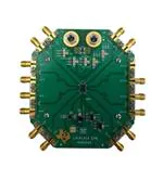
Figure 1. SN65LVCP1414 EVM
SLLU169 – July 20112
Submit Documentation Feedback
SN65LVCP1414 Evaluation Module (EVM)
Copyright © 20112, Texas Instruments Incorporated
5
�SN65LVCP1414 EVM Board Configuration
www.ti.com
J1
D2
D3
D4
USB
RST
RST
SUSPND
ONLINE
x
x
D1
R41
C4
C3
ON
SW2
U2
C15
x
R78
R66
R74
R75
R67
R68
R69
R70
R71
R72
R73
R49
R48
Q1
RST
R58
R59
C13
R60
R61
SW1
R47
R46
R45
R44
R43
R42
C12
R57
R56
R93
R96
R55
R54
R53
R52
U4
R92
C16
ECS D
12.0 MHz
x
R62
R63
R64
R65
R50
R51
C14
R91
R90
R17
R19
R21
R23
R25
R27
R29
R31
R33
R35
R37
R39
C1
R7
R9
R11
R13
R1
Figure 2. USB Dongle Board
6
SN65LVCP1414 Evaluation Module (EVM)
Copyright © 20112, Texas Instruments Incorporated
SLLU169 – July 20112
Submit Documentation Feedback
�Test Setup
www.ti.com
EQ0/ADD0
EQ1/ADD1
PWD#
GAIN
EQ_MODE/ADD2
DRV_PK#/SCL
I2C_EN
JMP8
VOD/CS
Figure 3. SN65LVCP1414 EVM Jumper Description
5
Test Setup
The EVM gives the developer two control interface options for operation, I2C or GPIO mode. Input and
output differential pairs are available through edge-launch SMAs with approximately 2.5 inches of trace
with Rogers Low–Dielectric material with 0.1-µF AC coupling capacitors. Apply power to the device, VCC,
using banana jacks (P1, P2).
SLLU169 – July 20112
Submit Documentation Feedback
SN65LVCP1414 Evaluation Module (EVM)
Copyright © 20112, Texas Instruments Incorporated
7
�I2C Mode
www.ti.com
Table 1. SN65LVCP1414 EVM Pin and Jumper Functionality Description
Description
Ref Des
Symbol
J1, J3
In0+, In0–
Differential input, channel 0
J5, J7
In1+, In1–
Differential input, channel 1
Differential input, channel 2
I2C mode
GPIO mode
J9, J11
In2+, In2–
J14, J16
In3+, In3–
Differential input, channel 3
J2, J4
Out0+, Out0–
Differential output, channel 0
J6, J8
Out1+, Out1–
Differential output, channel 1
J10, J12
Out2+, Out2–
Differential output, channel 2
J13, J15
Out3+, Out3–
Differential output, channel 3
P1
VCC
Banana jack, positive power-supply connection
P2
GND
Banana jack, ground power-supply connection
J17
USB
USB dongle connection
JMP1
VOD/CS
JMP2
PD#
JMP3
GAIN
High, sets the high VOD range
Low, sets the low VOD range
High, acts as chip select
Low, disables the I2C interface
High, normal operation
Low, power downs the device, inputs off and outputs disabled, resets the I2C
High, sets the high DC gain
Low, sets the low DC gain
Don't care
2
6
Configures the device in I C or GPIO mode of operation
High, enables I2C mode
Low, enables GPIO mode
JMP4
I2C_EN
JMP5
EQ1/ADD1
3-level control for EQ gain
I2C address
JMP6
EQ0/ADD0
3-level control for EQ gain
I2C address
JMP7
EQ_MODE/ADD2
3-level control for EQ gain
I2C address
JMP9
DRV_PK#/SCL
High, disables driver peaking
Low, enables driver 6 dB AC peaking
I2C SCL pin
I2C Mode
Implement I2C mode by using the SN65LVCP1414 GUI software provided in the CD-ROM with the EVM.
See the SN65LVCP1414 EVM GUI User’s Guide (SLLU170) for details on using the GUI. Table 2 shows
the appropriate jumpers settings on the EVM for configuring the device in I2C mode. Refer to Appendix A
for jumper shunt settings.
The USB dongle implementing TI’s TUSB3210 microcontroller, connected to the EVM board through the
Samtec MEC1 connector, is the preferred method of controlling the SN65LVCP1414 register stack and is
the only way to interface the GUI with the board.
See the SN65LVCP1414 datasheet (SLLSEC5) for a detailed description of the register map.
Table 2. SN65LVCP1414 EVM I2C Mode Settings
8
Ref Des
Symbol
I2C Mode Pin Settings
JMP1
VOD/CS
High, acts as chip select
JMP2
PD#
High, normal operation
Low, powers down the device, inputs off and outputs disabled, resets the I2C
JMP4
I2C_EN
High, enables I2C mode
JMP5
EQ1/ADD1
Low
JMP6
EQ0/ADD0
Low
JMP7
EQ_MODE/ADD2
Low
JMP9
DRV_PK#/SCL
Set in Mid position for SCL flow through from the USB card
SN65LVCP1414 Evaluation Module (EVM)
SLLU169 – July 20112
Submit Documentation Feedback
Copyright © 20112, Texas Instruments Incorporated
�GPIO Mode
www.ti.com
7
GPIO Mode
The SN65LVCP1414 is fully controllable in GPIO. Refer to Table 3 for the different jumper and EQ
settings. Table 4 shows the appropriate jumper and default settings on the EVM to configure and control
the device in GPIO mode. Refer to Appendix A for jumper shunt settings.
See the SN65LVCP1414 datasheet (SLLSEC5) for a detailed description of the control signals.
Table 3. SN65LVCP1414 EVM Jumper and EQ Settings
EQ1
EQ0
EQ Gain
GND
GND
000
GND
Hi-Z
000
GND
VCC
001
Hi-Z
GND
010
Hi-Z
Hi-Z
011
Hi-Z
VCC
100
VCC
GND
101
VCC
Hi-Z
110
VCC
VCC
111
EQ1/EQ0
Gain
DC Gain
(dB)
EQ Gain
(dB)
000 ~ 111
LOW
–6
1~9
000 ~ 111
Hi-Z
–6
7 ~ 17
000 ~ 111
HIGH
0
1~9
Table 4. SN65LVCP1414 EVM GPIO Mode Settings
Ref Des
Symbol
GPIO Mode Pin Description
JMP1
VOD/CS
High, sets the high VOD range
Low, sets the low VOD range
JMP2
PD#
High, normal operation
Low, power downs the device, inputs off and outputs disabled, resets the I2C
JMP3
GAIN
High, sets the high DC gain
Low, sets the low DC gain
JMP4
I2C_EN
Configures the device in I2C or GPIO mode of operation
High, enables I2C mode
Low, enables GPIO mode
JMP5
EQ1/ADD1
3 level control for EQ gain
JMP6
EQ0/ADD0
3 level control for EQ gain
JMP7
EQ_MODE/ADD2
3 level control for EQ gain
JMP9
DRV_PK#/SCL
High, disables driver peaking
Low, enables driver 6 dB AC peaking
SLLU169 – July 20112
Submit Documentation Feedback
SN65LVCP1414 Evaluation Module (EVM)
Copyright © 20112, Texas Instruments Incorporated
9
�Schematics
8
www.ti.com
Schematics
J1
C1
IN0P_SMA
IN0P_DUT
C2
J2
OUT0P_DUT
sma_edge
OUT0P_SMA
0.1uF
0.1uF
sma_edge
C3
IN0N_SMA
J3
IN0N_DUT
C4
OUT0N_DUT
OUT0N_SMA
0.1uF
sma_edge
sma_edge J4
0.1uF
J5
C5
IN1P_SMA
sma_edge
C6
OUT1P_DUT
IN1P_DUT
0.1uF
0.1uF
U1A
1
C7
IN1N_SMA
J7
sma_edge
IN1N_DUT
2
4
0.1uF
5
J9
C9
IN2P_SMA
sma_edge
IN2P_DUT
8
9
0.1uF
11
12
C11
IN2N_SMA
J11 sma_edge
J6
OUT1P_SMA
IN2N_DUT
IN0_P
OUT0_P
IN0_N
OUT0_N
IN1_P
IN1_N
OUT1_P
OUT1_N
IN2_P
OUT2_P
IN2_N
OUT2_N
IN3_P
OUT3_P
IN3_N
OUT3_N
31
30
C8
OUT1N_DUT
OUT1N_SMA
28
27
sma_edge J8
0.1uF
C10
OUT2P_DUT
J10
OUT2P_SMA
24
0.1uF
23
sma_edge
OUT2N_DUT
21
C12
20
OUT2N_SMA
0.1uF
0.1uF
LVCP1414_RGF
J14
C14
IN3P_SMA
sma_edge J12
LVCP1414_RGF
C13
OUT3P_DUT
sma_edge
sma_edge
U1B
J13
OUT3P_SMA
0.1uF
sma_edge
IN3P_DUT
0.1uF
C15
OUT3N_DUT
C16
IN3N_SMA
J16 sma_edge
OUT3N_SMA
0.1uF
sma_edge J15
IN3N_DUT
0.1uF
Figure 4. SN65LVCP1414 EVM Schematic, Sheet 1 Inputs and Outputs
10
SN65LVCP1414 Evaluation Module (EVM)
SLLU169 – July 20112
Submit Documentation Feedback
Copyright © 20112, Texas Instruments Incorporated
�Schematics
www.ti.com
VCC
VCC
VCC
VCC
SILKSCREEN
R1
DNI
R2
4.99k
HIGH
VOD/CS
LOW
SILKSCREEN
R3
NORMAL 4.99k
PWD#
POWERDOWN
JMP1
1
2
3
4
R4
DNI
JMP2
1
2
3
R5
DNI
4
R6
DNI
U1G
17
VCC
36
VCC
VOD/CS
PWD#
GAIN
REXT
37
18
LVCP1414_RGF
R7
DNI
R8
4.99k
R9
1.2k
JMP3
4
R10
DNI
1
2
3
SILKSCREEN
HIGH
GAIN
LOW
Figure 5. SN65LVCP1414 EVM Schematic, Sheet 2 GPIO Controls
SLLU169 – July 20112
Submit Documentation Feedback
SN65LVCP1414 Evaluation Module (EVM)
Copyright © 20112, Texas Instruments Incorporated
11
�Schematics
www.ti.com
VCC
VCC
SILKSCREEN
R11
DNI
R12
4.99k
VCC
I2C_MODE
I2C_EN
GPIO MODE
VCC
R13
4.99k
R14
4.99k
SILKSCREEN
JMP4
1
2
3
4
JMP5
1
2
3
EQ1_MID
4
U1F
R15
DNI
16
35
I2C_EN
EQ1/ADD1
EQ_MODE/ADD2
EQ0/ADD0
EQ1_PU
EQ1/ADD1
EQ1_PD
R16
4.99k
34
33
LVCP1414_RGF
VCC
VCC
VCC
VCC
R20
4.99k
R17
4.99k
R19
DNI
R18
4.99k
SILKSCREEN
JMP6
1
2
3
JMP7
4
1
2
3
4
EQ0_MID
EQ0_PU
EQ0/ADD0
EQ0_PD
R21
4.99k
R22
DNI
SILKSCREEN
CABLE_MODE
EQ_MODE/ADD2
TRACE MODE
Figure 6. SN65LVCP1414 EVM Schematic, Sheet 3 I2C Controls
12
SN65LVCP1414 Evaluation Module (EVM)
SLLU169 – July 20112
Submit Documentation Feedback
Copyright © 20112, Texas Instruments Incorporated
�Schematics
www.ti.com
USB INTERFACE
3P3V_USB
J17B
18
20
22
24
26
28
30
32
34
36
38
40
1
3
5
7
9
11
13
MEC1-120-02-F-D-A Connector
18
20
22
24
26
28
30
32
34
36
38
40
5V_USB
J17A
2
4
6
8
10
12
14
MEC1-120-02-F-D-A Connector
2
4
6
8
10
12
14
17
19
21
23
25
27
29
31
33
35
37
39
1
3
5
7
9
11
13
17
19
21
23
25
27
29
31
33
35
37
39
I2C CONTROL INTERFACE
GND
4
2
VCC
VCC
USB_I2C_SCL
R29
R30
0
0
8
1
2
VCCA
B1
A1
B2
A2
GND
OE
4.99k
4k
4k
4.99k
R26
R27
R28
U2
VCCB
R25
DNI_0
DNI_0
C17
1uF
C18
1uF
7
USB_I2C_SDA
VCC
3P3V_USB
R23
R24
JMP8 SCL
3
1
SDA
Header 2x2
3
U1E
14
5
15
4
6
JMP9
4
1
2
3
TXS0102DCT
SDA
DRV_PK#/SCL
LVCP1414_RGF
SILKSCREEN
HIGH
DRV_PK#/SCL
LOW
Figure 7. SN65LVCP1414 EVM Schematic, Sheet 4 I2C Communications
SLLU169 – July 20112
Submit Documentation Feedback
SN65LVCP1414 Evaluation Module (EVM)
Copyright © 20112, Texas Instruments Incorporated
13
�Schematics
www.ti.com
VCC
U1C
VCC
P1
3
6
7
10
13
19
22
25
26
29
32
38
1
VCC
Banana-Jack
C19
47uf
C20
22uf
P2
1
GND
Banana-Jack
VCC0
VCC1
VCC2
VCC3
VCC4
VCC5
VCC6
VCC7
VCC8
VCC9
VCC10
VCC11
LVCP1414_RGF
VCC
NOTE: Place near LVCP1414 device
C21
0.1uF
C22
0.1uF
U1D
VCC
GND_PAD
39
LVCP1414_RGF
C23
0.1uF
C24
0.1uF
C25
0.1uF
C26
0.1uF
C27
0.1uF
C28
0.1uF
C29
0.1uF
C30
0.1uF
Figure 8. SN65LVCP1414 EVM Schematic, Sheet 5 Power
14
SN65LVCP1414 Evaluation Module (EVM)
SLLU169 – July 20112
Submit Documentation Feedback
Copyright © 20112, Texas Instruments Incorporated
�Bill of Materials
www.ti.com
9
Bill of Materials
Table 5. SN65LVCP1414 EVM Bill of Materials
Reference
Value
Part
Part Number
Manufacturer
C1, C2, C3, C4, C5, C6, C7, C8,
C9, C10, C11, C12, C13, C14,
C15, C16, C21, C22, C23, C24,
C25, C26, C27, C28, C29, C30
0.1 µF
0201
LMK063BJ104KP-F
Taiyo Yuden
C17, C18
1.0 µF
0402
LMK105BJ105KV-F
Taiyo Yuden
C20
22 µF
1206
GCM31CR70J226KE23L
Murata Electronics North America
C19
47 µF
1210
LMK325BJ476MM-T
Taiyo Yuden
R29, R30
0.0 (Zero Ohm)
0402
ERJ-2GE0R00X
Panasonic - Ecg
R9
1.21 kΩ
0402
CR0402-16W-1211FT
Venkel
R26, R27, R28
4.02 kΩ
0402
CRCW04024K02FKED
Vishay/Dale
R2, R3, R8, R12, R13, R14, R16,
R17, R18, R20, R21
4.99 kΩ
0402
RG1005P-4991-B-T5
Susumu (VA)
U1
SN65LVCP1414RLJ
38-VQFN
SN65LVCP1414RLJ
Texas Instruments
U2
TXS0102DCTR
SM8
TXS0102DCT
Texas Instruments
JMP1, JMP2, JMP3, JMP4, JMP5,
JMP6, JMP7, JMP9
1X4T
0.1 in
HTSW-150-07-G-S
Samtec
JMP8
2X2
0.1 × 0.1 in
HTSW-150-07-G-D
Samtec
J17
SMT R/A
1.00 mm
MEC1-120-02-F-D-RA1-SL
Samtec
P1, P2
Banana Plug - Metal
4 mm
108-0740-001
Emerson Network Pwr
Connectivity
J1, J2, J3, J4, J5, J6, J7, J8, J9,
J10, J11, J12, J13, J14, J15, J16
32K243-40ML5
RF screw type
32K243-40ML5
Rosenberger
screws
0.25 in- Stainless Steel
4-40 Phillips panhead
PMSSS 440 0025 PH
Building Fasteners
standoff
0.75 in - Aluminum
4-40 Round - F/F
2029
Keystone Electronics
R1, R4, R5, R6, R7, R10, R11,
R15, R19, R22, R23, R24, R25
DNI
DNI
DNI
DNI
SLLU169 – July 20112
Submit Documentation Feedback
SN65LVCP1414 Evaluation Module (EVM)
Copyright © 20112, Texas Instruments Incorporated
15
�Board Layout
10
www.ti.com
Board Layout
Table 6. SN65LVCP1414 EVM PCB Layer Construction
NOTE: Always consult the board manufacturer for their process and design requirements
ensuring the desired impedance is achieved.
16
SN65LVCP1414 Evaluation Module (EVM)
Copyright © 20112, Texas Instruments Incorporated
SLLU169 – July 20112
Submit Documentation Feedback
�Board Layout
www.ti.com
Figure 9. SN65LVCP1414 Board Layout: Top Signal (Layer 1)
SLLU169 – July 20112
Submit Documentation Feedback
SN65LVCP1414 Evaluation Module (EVM)
Copyright © 20112, Texas Instruments Incorporated
17
�Board Layout
www.ti.com
Figure 10. SN65LVCP1414 Board Layout: Internal Ground (Layer 2)
18
SN65LVCP1414 Evaluation Module (EVM)
Copyright © 20112, Texas Instruments Incorporated
SLLU169 – July 20112
Submit Documentation Feedback
�Board Layout
www.ti.com
Figure 11. SN65LVDS1414 EVM Board Layout: Internal Power (Layer 3)
SLLU169 – July 20112
Submit Documentation Feedback
SN65LVCP1414 Evaluation Module (EVM)
Copyright © 20112, Texas Instruments Incorporated
19
�Board Layout
www.ti.com
Figure 12. SN65LVCP1414 Board Layout: Bottom Signal (Layer 4)
20
SN65LVCP1414 Evaluation Module (EVM)
Copyright © 20112, Texas Instruments Incorporated
SLLU169 – July 20112
Submit Documentation Feedback
�www.ti.com
Appendix A Jumper Shunt Settings
The table below shows the different shunt settings of the 3 and 4 pin jumpers on the EVM.
Shunt Setting
Description
High
HiZ
Low
High
Low
SLLU169 – July 20112
Submit Documentation Feedback
Jumper Shunt Settings
Copyright © 20112, Texas Instruments Incorporated
21
�EVALUATION BOARD/KIT/MODULE (EVM) ADDITIONAL TERMS
Texas Instruments (TI) provides the enclosed Evaluation Board/Kit/Module (EVM) under the following conditions:
The user assumes all responsibility and liability for proper and safe handling of the goods. Further, the user indemnifies TI from all claims
arising from the handling or use of the goods.
Should this evaluation board/kit not meet the specifications indicated in the User’s Guide, the board/kit may be returned within 30 days from
the date of delivery for a full refund. THE FOREGOING LIMITED WARRANTY IS THE EXCLUSIVE WARRANTY MADE BY SELLER TO
BUYER AND IS IN LIEU OF ALL OTHER WARRANTIES, EXPRESSED, IMPLIED, OR STATUTORY, INCLUDING ANY WARRANTY OF
MERCHANTABILITY OR FITNESS FOR ANY PARTICULAR PURPOSE. EXCEPT TO THE EXTENT OF THE INDEMNITY SET FORTH
ABOVE, NEITHER PARTY SHALL BE LIABLE TO THE OTHER FOR ANY INDIRECT, SPECIAL, INCIDENTAL, OR CONSEQUENTIAL
DAMAGES.
Please read the User's Guide and, specifically, the Warnings and Restrictions notice in the User's Guide prior to handling the product. This
notice contains important safety information about temperatures and voltages. For additional information on TI's environmental and/or safety
programs, please visit www.ti.com/esh or contact TI.
No license is granted under any patent right or other intellectual property right of TI covering or relating to any machine, process, or
combination in which such TI products or services might be or are used. TI currently deals with a variety of customers for products, and
therefore our arrangement with the user is not exclusive. TI assumes no liability for applications assistance, customer product design,
software performance, or infringement of patents or services described herein.
REGULATORY COMPLIANCE INFORMATION
As noted in the EVM User’s Guide and/or EVM itself, this EVM and/or accompanying hardware may or may not be subject to the Federal
Communications Commission (FCC) and Industry Canada (IC) rules.
For EVMs not subject to the above rules, this evaluation board/kit/module is intended for use for ENGINEERING DEVELOPMENT,
DEMONSTRATION OR EVALUATION PURPOSES ONLY and is not considered by TI to be a finished end product fit for general consumer
use. It generates, uses, and can radiate radio frequency energy and has not been tested for compliance with the limits of computing
devices pursuant to part 15 of FCC or ICES-003 rules, which are designed to provide reasonable protection against radio frequency
interference. Operation of the equipment may cause interference with radio communications, in which case the user at his own expense will
be required to take whatever measures may be required to correct this interference.
General Statement for EVMs including a radio
User Power/Frequency Use Obligations: This radio is intended for development/professional use only in legally allocated frequency and
power limits. Any use of radio frequencies and/or power availability of this EVM and its development application(s) must comply with local
laws governing radio spectrum allocation and power limits for this evaluation module. It is the user’s sole responsibility to only operate this
radio in legally acceptable frequency space and within legally mandated power limitations. Any exceptions to this are strictly prohibited and
unauthorized by Texas Instruments unless user has obtained appropriate experimental/development licenses from local regulatory
authorities, which is responsibility of user including its acceptable authorization.
For EVMs annotated as FCC – FEDERAL COMMUNICATIONS COMMISSION Part 15 Compliant
Caution
This device complies with part 15 of the FCC Rules. Operation is subject to the following two conditions: (1) This device may not cause
harmful interference, and (2) this device must accept any interference received, including interference that may cause undesired operation.
Changes or modifications not expressly approved by the party responsible for compliance could void the user's authority to operate the
equipment.
FCC Interference Statement for Class A EVM devices
This equipment has been tested and found to comply with the limits for a Class A digital device, pursuant to part 15 of the FCC Rules.
These limits are designed to provide reasonable protection against harmful interference when the equipment is operated in a commercial
environment. This equipment generates, uses, and can radiate radio frequency energy and, if not installed and used in accordance with the
instruction manual, may cause harmful interference to radio communications. Operation of this equipment in a residential area is likely to
cause harmful interference in which case the user will be required to correct the interference at his own expense.
�FCC Interference Statement for Class B EVM devices
This equipment has been tested and found to comply with the limits for a Class B digital device, pursuant to part 15 of the FCC Rules.
These limits are designed to provide reasonable protection against harmful interference in a residential installation. This equipment
generates, uses and can radiate radio frequency energy and, if not installed and used in accordance with the instructions, may cause
harmful interference to radio communications. However, there is no guarantee that interference will not occur in a particular installation. If
this equipment does cause harmful interference to radio or television reception, which can be determined by turning the equipment off and
on, the user is encouraged to try to correct the interference by one or more of the following measures:
• Reorient or relocate the receiving antenna.
• Increase the separation between the equipment and receiver.
• Connect the equipment into an outlet on a circuit different from that to which the receiver is connected.
• Consult the dealer or an experienced radio/TV technician for help.
For EVMs annotated as IC – INDUSTRY CANADA Compliant
This Class A or B digital apparatus complies with Canadian ICES-003.
Changes or modifications not expressly approved by the party responsible for compliance could void the user’s authority to operate the
equipment.
Concerning EVMs including radio transmitters
This device complies with Industry Canada licence-exempt RSS standard(s). Operation is subject to the following two conditions: (1) this
device may not cause interference, and (2) this device must accept any interference, including interference that may cause undesired
operation of the device.
Concerning EVMs including detachable antennas
Under Industry Canada regulations, this radio transmitter may only operate using an antenna of a type and maximum (or lesser) gain
approved for the transmitter by Industry Canada. To reduce potential radio interference to other users, the antenna type and its gain should
be so chosen that the equivalent isotropically radiated power (e.i.r.p.) is not more than that necessary for successful communication.
This radio transmitter has been approved by Industry Canada to operate with the antenna types listed in the user guide with the maximum
permissible gain and required antenna impedance for each antenna type indicated. Antenna types not included in this list, having a gain
greater than the maximum gain indicated for that type, are strictly prohibited for use with this device.
Cet appareil numérique de la classe A ou B est conforme à la norme NMB-003 du Canada.
Les changements ou les modifications pas expressément approuvés par la partie responsable de la conformité ont pu vider l’autorité de
l'utilisateur pour actionner l'équipement.
Concernant les EVMs avec appareils radio
Le présent appareil est conforme aux CNR d'Industrie Canada applicables aux appareils radio exempts de licence. L'exploitation est
autorisée aux deux conditions suivantes : (1) l'appareil ne doit pas produire de brouillage, et (2) l'utilisateur de l'appareil doit accepter tout
brouillage radioélectrique subi, même si le brouillage est susceptible d'en compromettre le fonctionnement.
Concernant les EVMs avec antennes détachables
Conformément à la réglementation d'Industrie Canada, le présent émetteur radio peut fonctionner avec une antenne d'un type et d'un gain
maximal (ou inférieur) approuvé pour l'émetteur par Industrie Canada. Dans le but de réduire les risques de brouillage radioélectrique à
l'intention des autres utilisateurs, il faut choisir le type d'antenne et son gain de sorte que la puissance isotrope rayonnée équivalente
(p.i.r.e.) ne dépasse pas l'intensité nécessaire à l'établissement d'une communication satisfaisante.
Le présent émetteur radio a été approuvé par Industrie Canada pour fonctionner avec les types d'antenne énumérés dans le manuel
d’usage et ayant un gain admissible maximal et l'impédance requise pour chaque type d'antenne. Les types d'antenne non inclus dans
cette liste, ou dont le gain est supérieur au gain maximal indiqué, sont strictement interdits pour l'exploitation de l'émetteur.
SPACER
SPACER
SPACER
SPACER
SPACER
SPACER
SPACER
SPACER
�【Important Notice for Users of this Product in Japan】
】
This development kit is NOT certified as Confirming to Technical Regulations of Radio Law of Japan
If you use this product in Japan, you are required by Radio Law of Japan to follow the instructions below with respect to this product:
1.
2.
3.
Use this product in a shielded room or any other test facility as defined in the notification #173 issued by Ministry of Internal Affairs and
Communications on March 28, 2006, based on Sub-section 1.1 of Article 6 of the Ministry’s Rule for Enforcement of Radio Law of
Japan,
Use this product only after you obtained the license of Test Radio Station as provided in Radio Law of Japan with respect to this
product, or
Use of this product only after you obtained the Technical Regulations Conformity Certification as provided in Radio Law of Japan with
respect to this product. Also, please do not transfer this product, unless you give the same notice above to the transferee. Please note
that if you could not follow the instructions above, you will be subject to penalties of Radio Law of Japan.
Texas Instruments Japan Limited
(address) 24-1, Nishi-Shinjuku 6 chome, Shinjuku-ku, Tokyo, Japan
http://www.tij.co.jp
【ご使用にあたっての注】
本開発キットは技術基準適合証明を受けておりません。
本製品のご使用に際しては、電波法遵守のため、以下のいずれかの措置を取っていただく必要がありますのでご注意ください。
1.
2.
3.
電波法施行規則第6条第1項第1号に基づく平成18年3月28日総務省告示第173号で定められた電波暗室等の試験設備でご使用いただく。
実験局の免許を取得後ご使用いただく。
技術基準適合証明を取得後ご使用いただく。
なお、本製品は、上記の「ご使用にあたっての注意」を譲渡先、移転先に通知しない限り、譲渡、移転できないものとします。
上記を遵守頂けない場合は、電波法の罰則が適用される可能性があることをご留意ください。
日本テキサス・インスツルメンツ株式会社
東京都新宿区西新宿6丁目24番1号
西新宿三井ビル
http://www.tij.co.jp
SPACER
SPACER
SPACER
SPACER
SPACER
SPACER
SPACER
SPACER
SPACER
SPACER
SPACER
SPACER
SPACER
SPACER
SPACER
SPACER
�EVALUATION BOARD/KIT/MODULE (EVM)
WARNINGS, RESTRICTIONS AND DISCLAIMERS
For Feasibility Evaluation Only, in Laboratory/Development Environments. Unless otherwise indicated, this EVM is not a finished
electrical equipment and not intended for consumer use. It is intended solely for use for preliminary feasibility evaluation in
laboratory/development environments by technically qualified electronics experts who are familiar with the dangers and application risks
associated with handling electrical mechanical components, systems and subsystems. It should not be used as all or part of a finished end
product.
Your Sole Responsibility and Risk. You acknowledge, represent and agree that:
1.
2.
3.
4.
You have unique knowledge concerning Federal, State and local regulatory requirements (including but not limited to Food and Drug
Administration regulations, if applicable) which relate to your products and which relate to your use (and/or that of your employees,
affiliates, contractors or designees) of the EVM for evaluation, testing and other purposes.
You have full and exclusive responsibility to assure the safety and compliance of your products with all such laws and other applicable
regulatory requirements, and also to assure the safety of any activities to be conducted by you and/or your employees, affiliates,
contractors or designees, using the EVM. Further, you are responsible to assure that any interfaces (electronic and/or mechanical)
between the EVM and any human body are designed with suitable isolation and means to safely limit accessible leakage currents to
minimize the risk of electrical shock hazard.
You will employ reasonable safeguards to ensure that your use of the EVM will not result in any property damage, injury or death, even
if the EVM should fail to perform as described or expected.
You will take care of proper disposal and recycling of the EVM’s electronic components and packing materials.
Certain Instructions. It is important to operate this EVM within TI’s recommended specifications and environmental considerations per the
user guidelines. Exceeding the specified EVM ratings (including but not limited to input and output voltage, current, power, and
environmental ranges) may cause property damage, personal injury or death. If there are questions concerning these ratings please contact
a TI field representative prior to connecting interface electronics including input power and intended loads. Any loads applied outside of the
specified output range may result in unintended and/or inaccurate operation and/or possible permanent damage to the EVM and/or
interface electronics. Please consult the EVM User's Guide prior to connecting any load to the EVM output. If there is uncertainty as to the
load specification, please contact a TI field representative. During normal operation, some circuit components may have case temperatures
greater than 60°C as long as the input and output are maintained at a normal ambient operating temperature. These components include
but are not limited to linear regulators, switching transistors, pass transistors, and current sense resistors which can be identified using the
EVM schematic located in the EVM User's Guide. When placing measurement probes near these devices during normal operation, please
be aware that these devices may be very warm to the touch. As with all electronic evaluation tools, only qualified personnel knowledgeable
in electronic measurement and diagnostics normally found in development environments should use these EVMs.
Agreement to Defend, Indemnify and Hold Harmless. You agree to defend, indemnify and hold TI, its licensors and their representatives
harmless from and against any and all claims, damages, losses, expenses, costs and liabilities (collectively, "Claims") arising out of or in
connection with any use of the EVM that is not in accordance with the terms of the agreement. This obligation shall apply whether Claims
arise under law of tort or contract or any other legal theory, and even if the EVM fails to perform as described or expected.
Safety-Critical or Life-Critical Applications. If you intend to evaluate the components for possible use in safety critical applications (such
as life support) where a failure of the TI product would reasonably be expected to cause severe personal injury or death, such as devices
which are classified as FDA Class III or similar classification, then you must specifically notify TI of such intent and enter into a separate
Assurance and Indemnity Agreement.
Mailing Address: Texas Instruments, Post Office Box 655303, Dallas, Texas 75265
Copyright © 2012, Texas Instruments Incorporated
�IMPORTANT NOTICE
Texas Instruments Incorporated and its subsidiaries (TI) reserve the right to make corrections, enhancements, improvements and other
changes to its semiconductor products and services per JESD46, latest issue, and to discontinue any product or service per JESD48, latest
issue. Buyers should obtain the latest relevant information before placing orders and should verify that such information is current and
complete. All semiconductor products (also referred to herein as “components”) are sold subject to TI’s terms and conditions of sale
supplied at the time of order acknowledgment.
TI warrants performance of its components to the specifications applicable at the time of sale, in accordance with the warranty in TI’s terms
and conditions of sale of semiconductor products. Testing and other quality control techniques are used to the extent TI deems necessary
to support this warranty. Except where mandated by applicable law, testing of all parameters of each component is not necessarily
performed.
TI assumes no liability for applications assistance or the design of Buyers’ products. Buyers are responsible for their products and
applications using TI components. To minimize the risks associated with Buyers’ products and applications, Buyers should provide
adequate design and operating safeguards.
TI does not warrant or represent that any license, either express or implied, is granted under any patent right, copyright, mask work right, or
other intellectual property right relating to any combination, machine, or process in which TI components or services are used. Information
published by TI regarding third-party products or services does not constitute a license to use such products or services or a warranty or
endorsement thereof. Use of such information may require a license from a third party under the patents or other intellectual property of the
third party, or a license from TI under the patents or other intellectual property of TI.
Reproduction of significant portions of TI information in TI data books or data sheets is permissible only if reproduction is without alteration
and is accompanied by all associated warranties, conditions, limitations, and notices. TI is not responsible or liable for such altered
documentation. Information of third parties may be subject to additional restrictions.
Resale of TI components or services with statements different from or beyond the parameters stated by TI for that component or service
voids all express and any implied warranties for the associated TI component or service and is an unfair and deceptive business practice.
TI is not responsible or liable for any such statements.
Buyer acknowledges and agrees that it is solely responsible for compliance with all legal, regulatory and safety-related requirements
concerning its products, and any use of TI components in its applications, notwithstanding any applications-related information or support
that may be provided by TI. Buyer represents and agrees that it has all the necessary expertise to create and implement safeguards which
anticipate dangerous consequences of failures, monitor failures and their consequences, lessen the likelihood of failures that might cause
harm and take appropriate remedial actions. Buyer will fully indemnify TI and its representatives against any damages arising out of the use
of any TI components in safety-critical applications.
In some cases, TI components may be promoted specifically to facilitate safety-related applications. With such components, TI’s goal is to
help enable customers to design and create their own end-product solutions that meet applicable functional safety standards and
requirements. Nonetheless, such components are subject to these terms.
No TI components are authorized for use in FDA Class III (or similar life-critical medical equipment) unless authorized officers of the parties
have executed a special agreement specifically governing such use.
Only those TI components which TI has specifically designated as military grade or “enhanced plastic” are designed and intended for use in
military/aerospace applications or environments. Buyer acknowledges and agrees that any military or aerospace use of TI components
which have not been so designated is solely at the Buyer's risk, and that Buyer is solely responsible for compliance with all legal and
regulatory requirements in connection with such use.
TI has specifically designated certain components which meet ISO/TS16949 requirements, mainly for automotive use. Components which
have not been so designated are neither designed nor intended for automotive use; and TI will not be responsible for any failure of such
components to meet such requirements.
Products
Applications
Audio
www.ti.com/audio
Automotive and Transportation
www.ti.com/automotive
Amplifiers
amplifier.ti.com
Communications and Telecom
www.ti.com/communications
Data Converters
dataconverter.ti.com
Computers and Peripherals
www.ti.com/computers
DLP® Products
www.dlp.com
Consumer Electronics
www.ti.com/consumer-apps
DSP
dsp.ti.com
Energy and Lighting
www.ti.com/energy
Clocks and Timers
www.ti.com/clocks
Industrial
www.ti.com/industrial
Interface
interface.ti.com
Medical
www.ti.com/medical
Logic
logic.ti.com
Security
www.ti.com/security
Power Mgmt
power.ti.com
Space, Avionics and Defense
www.ti.com/space-avionics-defense
Microcontrollers
microcontroller.ti.com
Video and Imaging
www.ti.com/video
RFID
www.ti-rfid.com
OMAP Applications Processors
www.ti.com/omap
TI E2E Community
e2e.ti.com
Wireless Connectivity
www.ti.com/wirelessconnectivity
Mailing Address: Texas Instruments, Post Office Box 655303, Dallas, Texas 75265
Copyright © 2012, Texas Instruments Incorporated
�