Product
Folder
Sample &
Buy
Support &
Community
Tools &
Software
Technical
Documents
TCA8418E
SCPS222C – MAY 2010 – REVISED OCTOBER 2015
TCA8418E I2C Controlled Keypad Scan IC With Integrated ESD Protection
1 Features
2 Applications
•
•
•
•
•
•
•
1
•
•
•
•
•
•
•
•
•
•
•
Operating Power-Supply Voltage Range of 1.65-V
to 3.6-V
±15-kV Human Body Model High Voltage ESD
(GPIO lines)
Supports 80 Buttons With Use of 18 GPIOs
Supports QWERTY Keypad Operation Plus GPIO
Expansion
Low Standby (Idle) Current Consumption: 3 μA
Supports 1-MHz Fast Mode Plus I2C Bus
10-Byte FIFO to Store 10 Key Presses and
Releases
Open-Drain Active-Low Interrupt Output
Integrated Debounce Time of 50 μs
Schmitt-Trigger Action Allows Slow Input
Transition and Better Switching Noise Immunity at
the SCL and SDA Inputs: Typical Vhys at 1.8 V is
0.18 V
Latch-Up Performance Exceeds 200 mA Per
JESD 78, Class II
Very Small Package
– WCSP (YFP): 2 mm × 2 mm; 0.4 mm pitch
Smart Phones
Tablets
HMI Panels
GPS Devices
MP3 Players
Digital Cameras
3 Description
The TCA8418E is a keypad scan device with
integrated ESD protection. It can operate from 1.65 V
to 3.6 V and has 18 general purpose inputs/outputs
(GPIO) that can be used to support up to 80 keys via
the I2C interface.
The TCA8418E saves power and bandwidths since it
handles the keypad scanning algorithms. The
TCA8418E is also ideal for usage with processors
that have limited GPIOs.
The key controller debounces inputs and maintains a
10 byte FIFO of key-press and release events which
can store up to 10 keys with overflow wrap capability.
An interrupt (INT) output can be configured to alert
key presses and releases either as they occur, or at
maximum rate. A CAD_INT pin is included to indicate
the detection of CTRL-ALT-DEL (essentially, 1, 11,
21) key press action.
Device Information(1)
PART NUMBER
TCA8418E
PACKAGE
BODY SIZE (NOM)
DSBGA (25)
2.00 mm × 2.00 mm
(1) For all available packages, see the orderable addendum at
the end of the data sheet.
Simplified Schematic
VCC
SDA
2
I C or SMBus Master
(e.g. Processor)
SCL
TCA8418E
INT
GND
ROW0
ROW1
ROW2
ROW3
COL0
COL1
COL2
1
2
3
4
5
6
7
8
9
*
0
#
Only 7 GPIOs are shown out of the full 18 GPIOs
1
An IMPORTANT NOTICE at the end of this data sheet addresses availability, warranty, changes, use in safety-critical applications,
intellectual property matters and other important disclaimers. PRODUCTION DATA.
�TCA8418E
SCPS222C – MAY 2010 – REVISED OCTOBER 2015
www.ti.com
Table of Contents
1
2
3
4
5
6
Features ..................................................................
Applications ...........................................................
Description .............................................................
Revision History.....................................................
Pin Configuration and Functions .........................
Specifications.........................................................
1
1
1
2
3
4
6.1
6.2
6.3
6.4
6.5
6.6
6.7
Absolute Maximum Ratings ..................................... 4
ESD Ratings ............................................................ 4
Recommended Operating Conditions....................... 4
Thermal Information .................................................. 5
Electrical Characteristics........................................... 5
I2C Interface Timing Requirements........................... 6
Reset Timing Requirements for Standard Mode, Fast
Mode, Fast Mode Plus (FM+) I2C Bus....................... 7
6.8 Switching Characteristics for Standard Mode, Fast
Mode, Fast Mode Plus (FM+) I2C Bus....................... 7
6.9 Keypad Switching Characteristics for Standard Mode,
Fast Mode, Fast Mode Plus (FM+) I2C Bus............... 7
6.10 Typical Characteristics ............................................ 8
7
8
Parameter Measurement Information ................ 11
Detailed Description ............................................ 15
8.1
8.2
8.3
8.4
8.5
8.6
9
Overview .................................................................
Functional Block Diagram .......................................
Feature Description.................................................
Device Functional Modes........................................
Programming ..........................................................
Register Maps ........................................................
15
15
15
20
21
25
Application and Implementation ........................ 36
9.1 Application Information............................................ 36
9.2 Typical Application .................................................. 38
10 Power Supply Recommendations ..................... 41
11 Layout................................................................... 43
11.1 Layout Guidelines ................................................. 43
11.2 Layout Example .................................................... 43
12 Device and Documentation Support ................. 44
12.1
12.2
12.3
12.4
Community Resources..........................................
Trademarks ...........................................................
Electrostatic Discharge Caution ............................
Glossary ................................................................
44
44
44
44
13 Mechanical, Packaging, and Orderable
Information ........................................................... 44
4 Revision History
NOTE: Page numbers for previous revisions may differ from page numbers in the current version.
Changes from Revision B (September 2010) to Revision C
•
Page
Added Pin Configuration and Functions section, ESD Ratings table, Feature Description section, Device Functional
Modes, Application and Implementation section, Power Supply Recommendations section, Layout section, Device
and Documentation Support section, and Mechanical, Packaging, and Orderable Information section ............................... 1
Changes from Revision A (June 2010) to Revision B
Page
•
Replaced ±8-kV with ±15-kV Human Body Model High Voltage ESD (GPIO lines) .............................................................. 1
•
Replaced all TBD values ........................................................................................................................................................ 5
2
Submit Documentation Feedback
Copyright © 2010–2015, Texas Instruments Incorporated
Product Folder Links: TCA8418E
�TCA8418E
www.ti.com
SCPS222C – MAY 2010 – REVISED OCTOBER 2015
5 Pin Configuration and Functions
YFP Package
25-Pin DSBGA
Laser Marking and Bump Views
E
E
D
D
C
C
B
B
A
A
5
4
3
2
1
1
3
2
4
5
Pin Assignments
E
INT
GND
COL5
COL0
ROW3
D
SCL
COL9
COL4
ROW0
ROW4
C
SDA
COL8
COL3
ROW1
ROW5
B
VCC
COL7
COL2
CAD_INT
ROW6
A
RESET
COL6
COL1
ROW2
ROW7
5
4
3
2
1
Pin Functions
PIN
I/O
DESCRIPTION
NO.
NAME
A1
ROW7
I/O
GPIO or row 7 in keypad matrix. If unused, connect to VCC through a pullup resistor.
A2
ROW2
I/O
GPIO or row 2 in keypad matrix. If unused, connect to VCC through a pullup resistor.
A3
COL1
I/O
GPIO or column 1 in keypad matrix. If unused, connect to VCC through a pullup resistor.
A4
COL6
I/O
GPIO or column 6 in keypad matrix. If unused, connect to VCC through a pullup resistor.
A5
RESET
I
B1
ROW6
I/O
GPIO or row 6 in keypad matrix
B2
CAD_INT
O
Active-low interrupt hardware output for 3-key simultaneous press-event. Open drain
structure. Connect to VCC through a pullup resistor.
B3
COL2
I/O
GPIO or column 2 in keypad matrix. If unused, connect to VCC through a pullup resistor.
B4
COL7
I/O
GPIO or column 7 in keypad matrix. If unused, connect to VCC through a pullup resistor.
B5
VCC
-
C1
ROW5
I/O
GPIO or row 5 in keypad matrix. If unused, connect to VCC through a pullup resistor.
C2
ROW1
I/O
GPIO or row 1 in keypad matrix. If unused, connect to VCC through a pullup resistor.
C3
COL3
I/O
GPIO or column 3 in keypad matrix. If unused, connect to VCC through a pullup resistor.
C4
COL8
I/O
GPIO or column 8 in keypad matrix. If unused, connect to VCC through a pullup resistor.
C5
SDA
I/O
Serial data bus. Connect to VCC through a pullup resistor.
D1
ROW4
I/O
GPIO or row 4 in keypad matrix. If unused, connect to VCC through a pullup resistor.
D2
ROW0
I/O
GPIO or row 0 in keypad matrix. If unused, connect to VCC through a pullup resistor.
D3
COL4
I/O
GPIO or column 4 in keypad matrix. If unused, connect to VCC through a pullup resistor.
D4
COL9
I/O
GPIO or column 9 in keypad matrix. If unused, connect to VCC through a pullup resistor.
D5
SCL
I
E1
ROW3
I/O
GPIO or row 3 in keypad matrix. If unused, connect to VCC through a pullup resistor.
E2
COL0
I/O
GPIO or column 0 in keypad matrix. If unused, connect to VCC through a pullup resistor.
E3
COL5
I/O
GPIO or column 5 in keypad matrix. If unused, connect to VCC through a pullup resistor.
Active-low reset input. Connect to VCC through a pullup resistor, if no active connection is
used.
Supply voltage of 1.65 V to 3.6 V
Serial clock bus. Connect to VCC through a pullup resistor.
Submit Documentation Feedback
Copyright © 2010–2015, Texas Instruments Incorporated
Product Folder Links: TCA8418E
3
�TCA8418E
SCPS222C – MAY 2010 – REVISED OCTOBER 2015
www.ti.com
Pin Functions (continued)
PIN
I/O
DESCRIPTION
NO.
NAME
E4
GND
–
Ground
E5
INT
O
Active-low interrupt output. Open drain structure. Connect to VCC through a pullup resistor.
6 Specifications
6.1 Absolute Maximum Ratings (1)
over operating free-air temperature range (unless otherwise noted)
VCC
Supply voltage
VI
Input voltage
(2)
Voltage range applied to any output in the high-impedance or power-off state
VO
(2)
Output voltage in the high or low state (2)
MIN
MAX
UNIT
–0.5
4.6
V
–0.5
4.6
V
–0.5
4.6
–0.5
4.6
V
IIK
Input clamp current
VI < 0
±20
mA
IOK
Output clamp current
VO < 0
±20
mA
IOL
Continuous output Low current
IOH
Continuous output High current
Tstg
Storage temperature
(1)
(2)
P port, SDA
INT
P port
50
VO = 0 to VCC
25
VO = 0 to VCC
mA
50
–65
150
°C
Stresses beyond those listed under Absolute Maximum Ratings may cause permanent damage to the device. These are stress ratings
only, and functional operation of the device at these or any other conditions beyond those indicated under Recommended Operating
Conditions is not implied. Exposure to absolute-maximum-rated conditions for extended periods may affect device reliability.
The input negative-voltage and output voltage ratings may be exceeded if the input and output current ratings are observed.
6.2 ESD Ratings
VALUE
Human-body model (HBM), per ANSI/ESDA/JEDEC JS-001 (Non-GPIO pins) (1)
V(ESD)
(1)
(2)
Electrostatic
discharge
UNIT
±2000
Charged-device model (CDM), per JEDEC specification JESD22-C101 (2)
±1000
Human-body model (HBM), per ANSI/ESDA/JEDEC JS-001 (GPIO pins) (1)
±15000
V
JEDEC document JEP155 states that 500-V HBM allows safe manufacturing with a standard ESD control process.
JEDEC document JEP157 states that 250-V CDM allows safe manufacturing with a standard ESD control process.
6.3 Recommended Operating Conditions
MIN
MAX
1.65
3.6
V
SCL, SDA, ROW0–7, COL0–9, RESET
0.7 × VCC
3.6
V
Low-level input voltage
SCL, SDA, ROW0–7, COL0–9, RESET
–0.5
0.3 × VCC
High-level output current
ROW0–7, COL0–9
10
mA
IOL
Low-level output current
ROW0–7, COL0–9
25
mA
TA
Operating free-air temperature
85
°C
VCC
Supply voltage
VIH
High-level input voltage
VIL
IOH
4
–40
Submit Documentation Feedback
UNIT
V
Copyright © 2010–2015, Texas Instruments Incorporated
Product Folder Links: TCA8418E
�TCA8418E
www.ti.com
SCPS222C – MAY 2010 – REVISED OCTOBER 2015
6.4 Thermal Information
over operating free-air temperature range (unless otherwise noted)
TCA8418E
THERMAL METRIC
(1)
YFP (DSBGA)
UNIT
25 PINS
RθJA
Junction-to-ambient thermal resistance
61.2
°C/W
RθJC(top)
Junction-to-case (top) thermal resistance
0.4
°C/W
RθJB
Junction-to-board thermal resistance
10.6
°C/W
ψJT
Junction-to-top characterization parameter
1.0
°C/W
ψJB
Junction-to-board characterization parameter
10.6
°C/W
RθJC(bot)
Junction-to-case (bottom) thermal resistance
N/A
°C/W
(1)
For more information about traditional and new thermal metrics, see the Semiconductor and IC Package Thermal Metrics application
report, SPRA953.
6.5 Electrical Characteristics
over recommended operating free-air temperature range, VCC = 1.65 V to 3.6 V (unless otherwise noted)
PARAMETER
VIK
Input diode clamp voltage
VPORR
Power-on reset voltage, VCC
rising
VPORF
Power-on reset voltage, VCC
falling
VCC
MIN
II = –18 mA
TEST CONDITIONS
1.65 V to 3.6 V
–1.2
VI = VCCP or GND, IO = 0
1.65 V to 3.6 V
IOH = –1 mA
IOH = –8 mA
VOH
ROW0–7, COL0–9 high-level
output voltage
IOH = –10 mA
IOL = 1 mA
IOL = 8 mA
VOL
ROW0–7, COL0–9 low-level
output voltage
IOL = 10 mA
1.43
0.76
1.15
V
1.65 V
1.25
1.65 V
1.2
2.3 V
1.8
3V
2.6
1.65 V
1.1
2.3 V
1.7
3V
2.5
V
1.65 V
0.4
1.65 V
0.45
2.3 V
0.25
3V
0.25
1.65 V
0.6
2.3 V
0.3
3V
0.25
VOL = 0.4 V
1.65 V to 3.6 V
3
INT and CAD_INT
VOL = 0.4 V
1.65 V to 3.6 V
3
II
SCL, SDA, ROW0–7,
COL0–9, RESET
VI = VCCI or GND
1.65 V to 3.6 V
RINT
Internal pullup resistor value
ROW0–7, COL0–9
Product Folder Links: TCA8418E
V
mA
1
55
Submit Documentation Feedback
Copyright © 2010–2015, Texas Instruments Incorporated
UNIT
V
1.03
SDA
IOL
TYP MAX
μA
kΩ
5
�TCA8418E
SCPS222C – MAY 2010 – REVISED OCTOBER 2015
www.ti.com
Electrical Characteristics (continued)
over recommended operating free-air temperature range, VCC = 1.65 V to 3.6 V (unless otherwise noted)
PARAMETER
TEST CONDITIONS
VCC
Oscillator
OFF
fSCL = 0 kHz
ICC
Supply
Voltage
18
1 key press
fSCL = 1 MHz
fSCL = 1 MHz
fSCL = 400 kHz
fSCL = 1 MHz
fSCL = 400 kHz
fSCL = 1 MHz
CI
SCL
SDA
Cio
(1)
ROW0–7, COL0–9
UNIT
13
Oscillator
ON
fSCL = 400 kHz
TYP MAX
1.65 V to 3.6 V
fSCL = 400 kHz
VI on SDA,
ROW0–7,
COL0–9 = VCC or
GND,
IO = 0, I/O =
inputs,
MIN
1.65 V
15
3.6 V
30
1.65 V
15
3.6 V
40
GPI low
(pullup
enable) (1)
GPI low
(pullup
disable)
μA
115
125
25
1.65 V to 3.6 V
35
115
1 GPO
active
125
VI = VCC or GND
1.65 V to 3.6 V
VIO = VCC or GND
1.65 V to 3.6 V
6
8
10
12.5
5
6
pF
pF
Assumes that one GPIO is enabled.
6.6 I2C Interface Timing Requirements
over recommended operating free-air temperature range (unless otherwise noted) (see Figure 16)
STANDARD MODE
I2C BUS
I2C clock frequency
fscl
2
tsch
I C clock high time
tscl
I2C clock low time
tsp
I2C spike time
2
tsds
I C serial data setup time
tsdh
I2C serial data hold time
ticr
I2C input rise time
ticf
I2C input fall time
FAST MODE
I2C BUS
FAST MODE PLUS (FM+)
I2C BUS
MIN
MAX
MIN
MAX
MIN
MAX
0
100
0
400
0
1000
4
0.6
0.26
4.7
1.3
0.5
50
50
100
50
0
0
0
2
μs
ns
ns
ns
(1)
300
120
ns
20 + 0.1Cb (1)
300
120
ns
(1)
300
120
μs
1000 20 + 0.1Cb
300
kHz
μs
50
250
UNIT
tocf
I C output fall time; 10 pF to 400 pF bus
tbuf
I2C bus free time between Stop and
Start
300 20 + 0.1Cb
4.7
1.3
0.5
μs
tsts
I2C Start or repeater Start condition
setup time
4.7
0.6
0.26
μs
2
tsth
I C Start or repeater Start condition hold
time
4
0.6
0.26
μs
tsps
I2C Stop condition setup time
4
0.6
0.26
μs
tvd(data)
Valid data time; SCL low to SDA output
valid
1
0.9
0.45
μs
tvd(ack)
Valid data time of ACK condition; ACK
signal from SCL low to SDA (out) low
1
0.9
0.45
μs
(1)
6
Cb = total capacitance of one bus line in pF
Submit Documentation Feedback
Copyright © 2010–2015, Texas Instruments Incorporated
Product Folder Links: TCA8418E
�TCA8418E
www.ti.com
SCPS222C – MAY 2010 – REVISED OCTOBER 2015
6.7 Reset Timing Requirements for Standard Mode, Fast Mode, Fast Mode Plus (FM+) I2C Bus
over recommended operating free-air temperature range (unless otherwise noted) (see Figure 19)
MIN
MAX
UNIT
(1)
μs
tW
Reset pulse duration
120
tREC
Reset recovery time
120 (1)
μs
tRESET
Time to reset
120 (1)
μs
(1)
The GPIO debounce circuit uses each GPIO input which passes through a two-stage register circuit. Both registers are clocked by the
same clock signal, presumably free-running, with a nominal period of 50 μs. When an input changes state, the new state is clocked into
the first stage on one clock transition. On the next same-direction transition, if the input state is still the same as the previously clocked
state, the signal is clocked into the second stage, and then on to the remaining circuits. Since the inputs are asynchronous to the clock,
it will take anywhere from zero to 50 μs after the input transition to clock the signal into the first stage. Therefore, the total debounce
time may be as long as 100 μs. Finally, to account for a slow clock, the spec further guard-banded at 120 μs.
6.8 Switching Characteristics for Standard Mode, Fast Mode, Fast Mode Plus (FM+) I2C Bus
PARAMETER
FROM
TO
Key event or Key
unlock or Overflow
tIV
GPI_INT with
Debounce_DIS_Low
Interrupt valid time
GPI_INT with
Debounce_DIS_High
ROW0–7,
COL0–9
CAD_INT
INT
INT, CAD_INT
SCL
INT
SCL
CAD_INT
SCL
ROW0–7,
COL0–9
MIN
MAX
20
60
40
120
10
30
20
60
UNIT
μs
tIR
Interrupt reset delay time
200
ns
tPV
Output data valid
400
ns
tPS
Input data setup time
P port
SCL
0
ns
tPH
Input data hold time
P port
SCL
300
ns
6.9 Keypad Switching Characteristics for Standard Mode, Fast Mode, Fast Mode Plus (FM+) I2C
Bus
PARAMETER
MIN
MAX
UNIT
Key press to detection delay
25
μs
Key release to detection delay
25
μs
7
s
Keypad unlock timer
Keypad interrupt mask timer
31
s
Debounce
60
ms
Submit Documentation Feedback
Copyright © 2010–2015, Texas Instruments Incorporated
Product Folder Links: TCA8418E
7
�TCA8418E
SCPS222C – MAY 2010 – REVISED OCTOBER 2015
www.ti.com
6.10 Typical Characteristics
TA = 25°C (unless otherwise noted)
12
1600
11
1400
10
V CC = 3.6 V
1200
Supply Current, I CC (nA)
Supply Current, I CC (µA)
9
V CC = 3.3 V
8
7
6
V CC = 2.5 V
5
4
V CC = 1.8 V
3
V CC = 3.6 V
1000
V CC = 3.3 V
800
V CC = 2.5 V
600
V CC = 1.8 V
400
V CC = 1.65 V
2
V CC = 1.65 V
200
1
0
-40
-15
10
35
60
0
-40
85
-15
Tem perature, TA (°C)
Figure 1. Supply Current vs Temperature
35
60
85
Figure 2. Standby Supply Current vs Temperature
11
60
V CC = 1.65 V
10
50
9
TA = -40°C
(mA)
8
40
TA = 25°C
SINK
7
6
Sink Current, I
Supply Current, I CC (uA)
10
Tem perature, TA (°C)
5
4
3
2
TA = 85°C
30
20
10
1
0
0
1.6
2.0
2.4
2.8
3.2
3.6
0.0
0.1
Supply Voltage, V CC (V)
0.2
Figure 3. Supply Current vs Supply Voltage
0.6
V CC = 2.5 V
60
TA = -40°C
TA = -40°C
80
50
TA = 25°C
(mA)
TA = 25°C
SINK
TA = 85°C
40
Sink Current, I
(mA)
0.5
100
V CC = 1.8 V
SINK
0.4
Figure 4. I/O Sink Current vs Output Low Voltage
(VCC = 1.65 V)
70
Sink Current, I
0.3
Output Low Voltage, V OL (V)
30
20
TA = 85°C
60
40
20
10
0
0
0.0
0.1
0.2
0.3
0.4
0.5
0.6
0.0
Figure 5. I/O Sink Current vs Output Low Voltage
(VCC = 1.8 V)
8
0.1
0.2
0.3
0.4
0.5
0.6
Output Low Voltage, V OL (V)
Output Low Voltage, V OL (V)
Figure 6. I/O Sink Current vs Output Low Voltage
(VCC = 2.5 V)
Submit Documentation Feedback
Copyright © 2010–2015, Texas Instruments Incorporated
Product Folder Links: TCA8418E
�TCA8418E
www.ti.com
SCPS222C – MAY 2010 – REVISED OCTOBER 2015
Typical Characteristics (continued)
TA = 25°C (unless otherwise noted)
140
120
V CC = 3.6 V
V CC = 3.3 V
120
TA = -40°C
(mA)
80
SINK
TA = 85°C
Sink Current, I
Sink Current, I
TA = -40°C
TA = 25°C
SINK
(mA)
100
60
40
20
100
TA = 25°C
TA = 85°C
80
60
40
20
0
0
0.0
0.1
0.2
0.3
0.4
0.5
0.0
0.6
0.1
0.2
0.3
0.4
0.5
0.6
Output Low Voltage, V OL (V)
Output Low Voltage, V OL (V)
Figure 7. I/O Sink Current vs Output Low Voltage
(VCC = 3.3 V)
Figure 8. I/O Sink Current vs Output Low Voltage
(VCC = 3.6 V)
120
20
V CC = 1.65 V
(-mA)
15
TA = 25°C
SOURCE
V CC = 1.8 V, IOL = 10 m A
Source Current, I
Output Low Voltage, V OL (mV)
TA = -40°C
90
V CC = 3.3 V, IOL = 10 m A
60
30
V CC = 1.8 V, IOL = 1 m A
0
-40
TA = 85°C
10
5
V CC = 3.3 V, IOL = 1 m A
0
-15
10
35
60
85
0.0
0.1
0.2
Tem perature, TA (°C)
Figure 9. I/O Low Voltage vs Temperature
0.5
0.6
36
V CC = 1.8 V
V CC = 2.5 V
TA = -40°C
(-mA)
TA = -40°C
18
27
TA = 25°C
SOURCE
TA = 25°C
SOURCE
(-mA)
0.4
Figure 10. I/O Source Current vs Output High Voltage
(VCC = 1.65 V)
24
TA = 85°C
Source Current, I
Source Current, I
0.3
V CCP - V OH (V)
12
6
TA = 85°C
18
9
0
0
0.0
0.1
0.2
0.3
0.4
0.5
0.6
0.0
0.1
0.2
0.3
0.4
0.5
0.6
V CCP - V OH (V)
V CCP - V OH (V)
Figure 11. I/O Source Current vs Output High Voltage
(VCC = 1.8 V)
Figure 12. I/O Source Current vs Output High Voltage
(VCC = 2.5 V)
Submit Documentation Feedback
Copyright © 2010–2015, Texas Instruments Incorporated
Product Folder Links: TCA8418E
9
�TCA8418E
SCPS222C – MAY 2010 – REVISED OCTOBER 2015
www.ti.com
Typical Characteristics (continued)
TA = 25°C (unless otherwise noted)
44
44
V CC = 3.6 V
V CC = 3.3 V
(-mA)
33
TA = 25°C
SOURCE
TA = 85°C
Source Current, I
Source Current, I
TA = -40°C
TA = 25°C
SOURCE
(-mA)
TA = -40°C
33
22
11
TA = 85°C
22
11
0
0
0.0
0.1
0.2
0.3
0.4
0.5
0.0
0.6
0.1
V CCP - V OH (V)
0.2
0.3
0.4
0.5
0.6
V CCP - V OH (V)
Figure 13. I/O Source Current vs Output High Voltage
(VCC = 3.3 V)
Figure 14. I/O Source Current vs Output High Voltage
(VCC = 3.6 V)
350
300
V CC = 1.8 V, IOH = -10 m A
V CC - V OH (mV)
250
200
V CC = 3.3 V, IOH = -10 m A
150
100
50
0
-40
-15
10
35
60
85
Tem perature, TA (°C)
Figure 15. I/O High Voltage vs Temperature
10
Submit Documentation Feedback
Copyright © 2010–2015, Texas Instruments Incorporated
Product Folder Links: TCA8418E
�TCA8418E
www.ti.com
SCPS222C – MAY 2010 – REVISED OCTOBER 2015
7 Parameter Measurement Information
VCC
RL = 1 kΩ
SDA
DUT
CL = 50 pF
SDA LOAD CONFIGURATION
Three Bytes for Complete
Device Programming
Stop
Condition
(P)
Start
Condition
(S)
Address
Address
Bit 7
Bit 6
(MSB)
Address
Bit 1
t scl
R/W
Bit 0
(LSB)
ACK
(A)
Data
Bit 07
(MSB)
Data
Bit 10
(LSB)
Stop
Condition
(P)
t sch
0.7 × VCC
SCL
0.3 × VCC
t icr
t icf
t buf
t sts
t PHL
t PLH
t sp
0.7 × VCC
SDA
0.3 × VCC
t icf
t icr
t sth
t sdh
t sds
t sps
Repeat
Start
Condition
Start or
Repeat
Start
Condition
Stop
Condition
VOLTAGE WAVEFORMS
BYTE
DESCRIPTION
1
I2C address
2, 3
P-port data
A.
CL includes probe and jig capacitance. tocf is measured with CL of 10 pF or 400 pF.
B.
All inputs are supplied by generators having the following characteristics: PRR ≤ 10 MHz, ZO = 50 Ω, tr/tf ≤ 30 ns.
C.
All parameters and waveforms are not applicable to all devices.
Figure 16. I2C Interface Load Circuit and Voltage Waveforms
Submit Documentation Feedback
Copyright © 2010–2015, Texas Instruments Incorporated
Product Folder Links: TCA8418E
11
�TCA8418E
SCPS222C – MAY 2010 – REVISED OCTOBER 2015
www.ti.com
Parameter Measurement Information (continued)
VCC
RL = 4.7 kW
INT
DUT
CL = 100 pF
(see Note A)
INTERRUPT LOAD CONFIGURATION
ACK
From Slave
Start
Condition
8 Bits
(One Data Byte)
From Port
R/W
Slave Address
S
0
1
1
0
1
0
0
1
A
1
2
3
4
5
6
7
8
A
Data 1
ACK
From Slave
Data From Port
A
Data 2
1
P
A
tir
tir
B
B
INT
tiv
A
tsps
A
Data
Into
Port
Address
Data 1
0.5 ´ VCC
INT
SCL
Data 2
0.7 ´ VCC
R/W
tiv
A
0.3 ´ VCC
tir
0.5 ´ VCC
Pn
0.5 ´ VCC
INT
View A−A
View B−B
A.
CL includes probe and jig capacitance.
B.
All inputs are supplied by generators having the following characteristics: PRR ≤ 10 MHz, ZO = 50 Ω, tr/tf ≤ 30 ns.
C.
All parameters and waveforms are not applicable to all devices.
Figure 17. Interrupt Load Circuit and Voltage Waveforms
12
Submit Documentation Feedback
Copyright © 2010–2015, Texas Instruments Incorporated
Product Folder Links: TCA8418E
�TCA8418E
www.ti.com
SCPS222C – MAY 2010 – REVISED OCTOBER 2015
Parameter Measurement Information (continued)
Pn
500 W
DUT
2 ´ VCC
CL = 50 pF
(see Note A)
500 W
P-PORT LOAD CONFIGURATION
SCL
P0
A
P3
0.7 ´ VCC
0.3 ´ VCC
Slave
ACK
SDA
tpv
(see Note B)
Pn
Unstable
Data
Last Stable Bit
WRITE MODE (R/W = 0)
SCL
0.7 ´ VCC
P0
A
tps
P3
0.3 ´ VCC
tph
Pn
0.5 ´ VCC
READ MODE (R/W = 1)
A.
CL includes probe and jig capacitance.
B.
tpv is measured from 0.7 × VCC on SCL to 50% I/O (Pn) output.
C.
All inputs are supplied by generators having the following characteristics: PRR ≤ 10 MHz, ZO = 50 Ω, tr/tf ≤ 30 ns.
D.
The outputs are measured one at a time, with one transition per measurement.
E.
All parameters and waveforms are not applicable to all devices.
Figure 18. P Port Load Circuit and Timing Waveforms
Submit Documentation Feedback
Copyright © 2010–2015, Texas Instruments Incorporated
Product Folder Links: TCA8418E
13
�TCA8418E
SCPS222C – MAY 2010 – REVISED OCTOBER 2015
www.ti.com
Parameter Measurement Information (continued)
VCC
RL = 1 kW
500 W
Pn
SDA
DUT
DUT
CL = 50 pF
(see Note A)
SDA LOAD CONFIGURATION
2 ´ VCC
CL = 50 pF
(see Note A)
500 W
P-PORT LOAD CONFIGURATION
Start
SCL
ACK or Read Cycle
SDA
0.3 ´ VCC
tRESET
VCC/2
RESET
tREC
tREC
tW
VCC/2
Pn
tRESET
A.
CL includes probe and jig capacitance.
B.
All inputs are supplied by generators having the following characteristics: PRR ≤ 10 MHz, ZO = 50 Ω, tr/tf ≤ 30 ns.
C.
The outputs are measured one at a time, with one transition per measurement.
D.
I/Os are configured as inputs.
E.
All parameters and waveforms are not applicable to all devices.
Figure 19. Reset Load Circuits and Voltage Waveforms
14
Submit Documentation Feedback
Copyright © 2010–2015, Texas Instruments Incorporated
Product Folder Links: TCA8418E
�TCA8418E
www.ti.com
SCPS222C – MAY 2010 – REVISED OCTOBER 2015
8 Detailed Description
8.1 Overview
The TCA8418E supports up to 10 columns by 8 rows of keys, up to 80 keys. Any combination of these rows and
columns can be configured to be added to the keypad matrix. This is done by setting the appropriate rows and
columns to a value of 1 in the corresponding KP_GPIO registers (seen in Table 9). Once the rows and columns
that are connected to the keypad matrix are added to the keypad array, then the TCA8418E will begin monitoring
the keypad array, and any configured general purpose inputs (GPIs).
8.2 Functional Block Diagram
Interrupt
Control
INT
SCL
SDA
I2C Bus
Control
VCC
Power-On
Reset
Control
Registers
and FIFO
Keypad
Control
ROW0–COL9
Oscillator
(32 kHz)
RESET
Figure 20. Logic Diagram (Positive Logic)
8.3 Feature Description
8.3.1 Key Events
8.3.1.1 Key Event Table
The TCA8418E can be configured to support many different configurations of keypad setups. All 18 GPIOs for
the rows and columns can be used to support up to 80 keys in a key pad array. Another option is that all 18
GPIOs be used for GPIs to read 18 buttons which are not connected in an array. Any combination in between is
also acceptable (for example, a 3 x 4 keypad matrix and using the remaining 11 GPIOs as a combination of
inputs and outputs).
For both types of inputs (keypad matrix and a GPI), a key event can be added to the key event FIFO. The values
that are added to the FIFO depend on the configuration (keypad array or GPI) and on which port the press was
read on. The tables below show the values that correspond to both types of configurations.
Key values below are represented in decimal values, because the 10s place is used to mark the row, and the
ones place is used to denote the column. It is more clear to see the numbering convention used when viewed in
decimal values.
Submit Documentation Feedback
Copyright © 2010–2015, Texas Instruments Incorporated
Product Folder Links: TCA8418E
15
�TCA8418E
SCPS222C – MAY 2010 – REVISED OCTOBER 2015
www.ti.com
Table 1. Key Event Table (Keypad Array)
C0
C1
C2
C3
C4
C5
C6
C7
C8
C9
R0
1
2
3
4
5
6
7
8
9
10
R1
11
12
13
14
15
16
17
18
19
20
R2
21
22
23
24
25
26
27
28
29
30
R3
31
32
33
34
35
36
37
38
39
40
R4
41
42
43
44
45
46
47
48
49
50
R5
51
52
53
54
55
56
57
58
59
60
R6
61
62
63
64
65
66
67
68
69
70
R7
71
72
73
74
75
76
77
78
79
80
Table 2. Key Event Table (Row GPI Events)
R0
R1
R2
R3
R4
R5
R6
R7
97
98
99
100
101
102
103
104
Table 3. Key Event Table (Column GPI Events)
C0
C1
C2
C3
C4
C5
C6
C7
C8
C9
105
106
107
108
109
110
111
112
113
114
8.3.1.2 General Purpose Input (GPI) Events
A column or row configured as GPI can be programmed to be part of the Key Event Table, hence becomes also
capable of generating Key Event Interrupt. A Key Event Interrupt caused by a GPI follow the same process flow
as a Key Event Interrupt caused by a Key press.
GPIs configured as part of the Key Event Table allows for single key switches to be monitored as well as other
GPI interrupts. As part of the Event Table, GPIs are represented with decimal value of 97 and run through
decimal value of 114. R0-R7 are represented by 97-104 and C0-C9 are represented by 105-114
For a GPI that is set as active high, and is enabled in the Key Event Table, the state-machine will add an event
to the event count and event table whenever that GPI goes high. If the GPI is set to active low, a transition from
high to low will be considered a press and will also be added to the event count and event table. Once the
interrupt state has been met, the state machine will internally set an interrupt for the opposite state programmed
in the register to avoid polling for the released state, hence saving current. Once the released state is achieved,
it will add it to the event table. The press and release will still be indicated by bit 7 in the event register.
The GPI Events can also be used as unlocked sequences. When the GPI_EM bit is set, GPI events will not be
tracked when the keypad is locked. GPI_EM bit must be cleared for the GPI events to be tracked in the event
counter and table when the keypad is locked.
8.3.1.3 Key Event (FIFO) Reading
The TCA8418E has a 10-byte event FIFO, which stores any key presses or releases which have been
configured to be added to the Key Event Table. All ROWs and COLs added to the keypad matrix via the
KP_GPIO1-3 Registers will have any key pad events added to the FIFO. Any GPIs configured with a 1 in the
GPI_EM1-3 Registers will also be part of the event FIFO.
When the host wishes to read the FIFO, the following procedure is recommended.
1. Read the INT_STAT (0x02) register to determine what asserted the INT line. If GPI_INT or K_INT is set, then
a key event has occurred, and the event is stored in the FIFO.
2. Read the KEY_LCK_EC (0x03) register, bits [3:0] to see how many events are stored in FIFO.
3. Read the KEY_EVENT_A (0x04) register. Bit 7 value '0' signifies key release, value 1 signifies key press.
Bits [6:0] state which key was pressed with respect to the Key Event Table. With each read of the key event
register, the event counter in KEY_LCK_EC[3:0] will decrease by 1, and the FIFO will shift the events down 1
register.
4. Repeat step 3 until either KEY_LCK_EC[3:0] = 0 or KEY_EVENT_A = 0. This signifies that the FIFO is
empty.
16
Submit Documentation Feedback
Copyright © 2010–2015, Texas Instruments Incorporated
Product Folder Links: TCA8418E
�TCA8418E
www.ti.com
SCPS222C – MAY 2010 – REVISED OCTOBER 2015
5. Reset the INT_STAT interrupt flag which was causing the interrupt by writing a 1 to the specific bit.
As an example, consider the following key presses.
Table 4. Example Key Sequence
EVENT NUMBER
KEY (DECIMAL VALUE)
PRESS/RELEASE
1
1
Press
2
32
Press
3
1
Release
4
32
Release
5
23
Press
6
23
Release
7
45
Press
8
41
Press
9
41
Release
10
45
Release
If this example key sequence occurs, then while performing the recommended read procedure listed above, the
host would see the following information. Information at the top of the list is of an initial read to the
KEY_LCK_EC[3:0] register.
Table 5. Example Key Sequence
KEY_LCK_EC[3:0] VALUE
KEY_EVENT_A VALUE
(BINARY/HEX)
KEY (DECIMAL VALUE)
PRESS/RELEASE
10
N/A
N/A
N/A
Press
9
1 000 0001 (0x81)
1
8
1 010 0000 (0xA0)
32
Press
7
0 000 0001 (0x01)
1
Release
6
0 010 0000 (0x20)
32
Release
5
1 001 0111 (0x97)
23
Press
4
0 001 0111 (0x17)
23
Release
3
1 010 1101 (0xAD)
45
Press
2
1 010 1001 (0xA9)
41
Press
1
0 010 1001 (0x29)
41
Release
0
0 010 1101 (0x2D)
45
Release
8.3.1.4 Key Event Overflow
The TCA8418E has the ability to handle an overflow of the key event FIFO. An overflow event occurs when the
FIFO is full of events (10 key events are stored) and a new key event occurs. In short, this means that the
TCA8418E does not have the ability to hold any more key press information in the internal buffer. When this
occurs, the OVR_FLOW_INT bit in the INT_STAT Register is set, and if the OVR_FLOW_IEN bit is set in the
CFG Register, then the INT output will be asserted low to let the processor know that an overflow has occurred.
The TCA8418E has the ability to handle an overflow in 1 of two ways, which is determined by the bit value of the
OVR_FLOW_M bit in the CFG Register.
Table 6. OVR_FLOW_M Bit
OVR_FLOW_M VALUE
OVERFLOW MODE
BEHAVIOR
1
Enabled
Overflow data shifts with last event pushing first event out
0
Disabled (Default)
Overflow data is not stored and lost
Submit Documentation Feedback
Copyright © 2010–2015, Texas Instruments Incorporated
Product Folder Links: TCA8418E
17
�TCA8418E
SCPS222C – MAY 2010 – REVISED OCTOBER 2015
www.ti.com
Consider the example below, if the FIFO is full of the key presses and a new key press comes in. This new
overflow key press will be a key press of key 2 (0x82 is the hex representation of a key 2 press event)
Table 7. Key Event Overflow Handling
AFTER KEY 1 PRESS EVENT (0x82)
FIFO REGISTER
ORIGINAL VALUE
A
0x81
0xA0
0x81
B
0xA0
0x01
0xA0
C
0x01
0x20
0x01
D
0x20
0x97
0x20
E
0x97
0x17
0x97
F
0x17
0xAD
0x17
H
0xAD
0xA9
0xAD
I
0xA9
0x29
0xA9
J
0x29
0x2D
0x29
K
0x2D
0x82
0x2D
OVR_FLOW_M = 1
OVR_FLOW_M = 0
8.3.2 Keypad Lock/Unlock
This user can lock the keypad through the lock/unlock feature in this device. Once the keypad is locked by
setting BIT6 in KEY_LCK_EC, it can prevent the generation of key event interrupts and recorded key events. The
unlock keys can be programmed with any value of the keys in the keypad matrix or any general purpose input
(GPI) values that are part of the Key Event Table. When the keypad lock interrupt mask timer is non-zero, the
user will need to press two specific keys before an keylock interrupt is generated or keypad events are recorded.
A key event interrupt is generated the first time a user presses any key. This first interrupt can be used to turn on
an LCD and display the unlock message. The processor will then read the lock status register to see if the
keypad is unlocked. The next interrupt (keylock interrupt) will not be generated unless both unlock keys
sequences are correct. If correct Unlock keys are not pressed before the mask timer expires, the state machine
will start over again.
The recommended procedure to lock the keypad is to do the following
1. Determine which keys will be used for the unlock sequence. The key value from the Key Event Tables needs
to be entered into the UNLOCK1 and UNLOCK2 registers.
2. The UNLOCK1 to UNLOCK2 timer duration must be set by entering the desired seconds (valid range is 0 to
7 seconds) into bits [2:0] of the KP_LCK_TMR register.
3. If an interrupt mask is desired (see Keypad Lock Interrupt Mask Timer), then the desired interrupt mask
duration (valid range is 0 to 31 seconds) must be entered into bits [7:3] of the KP_LCK_TMR register.
4. When the host is ready to lock the keypad, a 1 is to be written to the K_LCK_EN bit (BIT6) in the
KEY_LCK_EC register. This will lock the keypad.
5. If the host wishes to manually unlock the keypad, writing a '0' to the K_LCK_EN bit (BIT6) in the
KEY_LCK_EC register will unlock the keypad.
18
Submit Documentation Feedback
Copyright © 2010–2015, Texas Instruments Incorporated
Product Folder Links: TCA8418E
�TCA8418E
www.ti.com
SCPS222C – MAY 2010 – REVISED OCTOBER 2015
Key Press / Start
Generate KE_INT
NO
KP_LCK_TIMER
[7:3] == 0
YES
Start Mask Timer
Countdown
NO
First Unlock Key
Pressed
NO
YES
YES
Mask Timer
Countdown
Expired
NO
First Unlock Key
Pressed
Start Unlock1 to
Unlock2 Timer
YES
YES
Start Unlock1 to
Unlock2 Timer
Unlock1 to
Unlock2 Timer
Expired
NO
YES
Mask Timer
Countdown
Expired
NO
Unlock1 to
Unlock2 Timer
Expired
YES
Second Unlock
Key Pressed
NO
NO
YES
Second Unlock
Key Pressed
NO
YES
Unlock Keypad
Unlock Keypad
Generate
K_LCK_INT
Generate
K_LCK_INT
Figure 21. Keypad Lock Flowchart
8.3.3 Keypad Lock Interrupt Mask Timer
The TCA8418E features a Keypad Lock/Unlock feature which allows the user to stop the generation of key event
interrupts by locking the key pad. There is an interrupt mask timer feature with the keypad lock, which allows the
generation of a single interrupt when a key is pressed, primarily for the purpose of LCD backlighting. Note that
this interrupt mask timer can also be used to limit the number of interrupts generated for a given amount of time.
The interrupt mask timer is enabled by setting bits [7:3] of the KP_LCK_TIMER register. The value in this register
can be anywhere from 0 to 31 seconds (note that a value of 0 will disable this interrupt mask feature). When a
keypad is locked and the interrupt mask timer is set to a non-zero value, this will enable the interrupt mask timer.
This interrupt mask timer limits the amount of interrupts generated. Typically, this is used with the Keypad
Lock/Unlock feature for LCD back lights. It is easiest to explain this feature with the following example; A mobile
device has a LCD screen with a back light display which turns off after 10 seconds to save power. Normally, an
interrupt to the processor would tell this LCD back light to turn on. When the keypad is locked, no interrupts are
generated, so the back light will never turn on. This is where the interrupt mask feature is used. Please refer to
Figure 21. The procedure for an example is below.
1. Since the back light turns off after 10 seconds of no interrupts, the interrupt mask timer (
KP_LCK_TIMER[7:3] ) gets set to 10 seconds. Keypad is then locked.
2. When the first key press is detected, the TCA8418E sends an interrupt to the processor and starts a 10
second count down.
3. If the correct unlock sequence is not entered within the 10 seconds, no interrupts are sent and the back light
will turn off.
Submit Documentation Feedback
Copyright © 2010–2015, Texas Instruments Incorporated
Product Folder Links: TCA8418E
19
�TCA8418E
SCPS222C – MAY 2010 – REVISED OCTOBER 2015
www.ti.com
4. After the 10 second timer has expired, if another key press occurs while keypad is locked (regardless of
whether it is a correct unlock key or not), another interrupt is generated and the 10 second count down
begins again.
8.3.4 Control-Alt-Delete Support
The TCA8418E can support normal key presses, but it also can support a (CAD) key press.
This feature allows the host to recognize a specific key press and alert the host that the combination has
occurred. The TCA8418E will recognize a key press if keys 1, 11, and 21 are all pressed at the
same time. These keys are referenced to the key values listed in the Key Event Table. Note that this key
combination that triggers a CAD interrupt is not adjustable, and must be keys 1, 11, and 21. On the YFP
package, there is an additional CAD_INT output, which will be asserted low when the keys are
pressed at the same time.
8.3.5 Interrupt Output
An interrupt is generated by any rising or falling edge of the port inputs in the input mode. After time tiv, the signal
INT is valid. Resetting the interrupt circuit is achieved when data on the port is changed to the original setting or
data is read from the port that generated the interrupt. Resetting occurs in the read mode at the acknowledge
(ACK) or not acknowledge (NACK) bit after the rising edge of the SCL signal. Interrupts that occur during the
ACK or NACK clock pulse can be lost (or be very short) due to the resetting of the interrupt during this pulse.
Each change of the I/Os after resetting is detected and is transmitted as INT.
Reading from or writing to another device does not affect the interrupt circuit, and a pin configured as an output
cannot cause an interrupt. Changing an I/O from an output to an input may cause a false interrupt to occur, if the
state of the pin does not match the contents of the input port register.
The INT output has an open-drain structure and requires a pullup resistor to VCC depending on the application. If
the INT signal is connected back to the processor that provides the SCL signal to the TCA8418E, then the INT
pin has to be connected to VCC. If not, the INT pin can be connected to VCCP.
8.3.5.1 50-µs Interrupt Configuration
The TCA8418E provides the capability of deasserting the interrupt for 50 μs while there is a pending event.
When the INT_CFG bit in Register 0x01 is set, any attempt to clear the interrupt bit while the interrupt pin is
already asserted results in a 50 μs deassertion. When the INT_CFG bit is cleared, INT remains asserted if the
host tries to clear the interrupt. This feature is particularly useful for software development and edge triggering
applications.
8.4 Device Functional Modes
8.4.1 Power-On Reset (POR)
When power (from 0 V) is applied to VCC, an internal power-on reset circuit holds the TCA8418E in a reset
condition until VCC has reached VPORR. At that time, the reset condition is released, and the TCA8418E registers
and I2C/SMBus state machine initialize to their default states. After that, VCC must be lowered to below VPORF
and back up to the operating voltage for a power-reset cycle. See Power Supply Recommendations for more
information on power up reset requirements.
8.4.2 Powered (Key Scan Mode)
The TCA8418E can be used to read GPI from single buttons, or configured in key scan mode to read an array of
keys. In key scan mode, there are two modes of operation.
8.4.2.1 Idle Key Scan Mode
Once the TCA8418E has had the keypad array configured, it will enter idle mode when no keys are being
pressed. All columns configured as part of the keypad array will be driven low and all rows configured as part of
the keypad array will be set to inputs, with pullup resistors enabled. During idle mode, the internal oscillator is
turned off so that power consumption is low as the device awaits a key press.
20
Submit Documentation Feedback
Copyright © 2010–2015, Texas Instruments Incorporated
Product Folder Links: TCA8418E
�TCA8418E
www.ti.com
SCPS222C – MAY 2010 – REVISED OCTOBER 2015
Device Functional Modes (continued)
8.4.2.2 Active Key Scan Mode
When the TCA8418E is in idle key scan mode, the device awaits a key press. Once a key is pressed in the
array, a low signal on one of the ROW pin inputs triggers an interrupt, which will turn on the internal oscillator
and enter the active key scan mode. At this point, the TCA8418E will start the key scan algorithm to determine
which key is being pressed, and/or it will use the internal oscillator for debouncing. Once all keys have been
released, the device will enter idle key scan mode.
8.5 Programming
8.5.1 I2C Interface
The TCA8418E has a standard bidirectional I2C interface that is controlled by a master device in order to be
configured or read the status of this device. Each slave on the I2C bus has a specific device address to
differentiate between other slave devices that are on the same I2C bus. Many slave devices will require
configuration upon startup to set the behavior of the device. This is typically done when the master accesses
internal register maps of the slave, which have unique register addresses. A device can have one or multiple
registers where data is stored, written, or read.
The physical I2C interface consists of the serial clock (SCL) and serial data (SDA) lines. Both SDA and SCL lines
must be connected to VCC through a pullup resistor. The size of the pullup resistor is determined by the amount
of capacitance on the I2C lines. (For further details, refer to I2C pullup Resistor Calculation (SLVA689).) Data
transfer may be initiated only when the bus is idle. A bus is considered idle if both SDA and SCL lines are high
after a STOP condition.
The following is the general procedure for a master to access a slave device:
1. If a master wants to send data to a slave:
– Master-transmitter sends a START condition and addresses the slave-receiver.
– Master-transmitter sends data to slave-receiver.
– Master-transmitter terminates the transfer with a STOP condition.
2. If a master wants to receive or read data from a slave:
– Master-receiver sends a START condition and addresses the slave-transmitter.
– Master-receiver sends the requested register to read to slave-transmitter.
– Master-receiver receives data from the slave-transmitter.
Submit Documentation Feedback
Copyright © 2010–2015, Texas Instruments Incorporated
Product Folder Links: TCA8418E
21
�TCA8418E
SCPS222C – MAY 2010 – REVISED OCTOBER 2015
www.ti.com
Programming (continued)
– Master-receiver terminates the transfer with a STOP condition.
SCL
SDA
Data Transfer
START
Condition
STOP
Condition
Figure 22. Definition of Start and Stop Conditions
SDA line stable while SCL line is high
SCL
1
0
1
0
1
0
1
0
ACK
MSB
Bit
Bit
Bit
Bit
Bit
Bit
LSB
ACK
SDA
Byte: 1010 1010 ( 0xAAh )
Figure 23. Bit Transfer
8.5.2 Bus Transactions
Data must be sent to and received from the slave devices, and this is accomplished by reading from or writing to
registers in the slave device.
Registers are locations in the memory of the slave which contain information, whether it be the configuration
information or some sampled data to send back to the master. The master must write information to these
registers in order to instruct the slave device to perform a task.
While it is common to have registers in I2C slaves, note that not all slave devices will have registers. Some
devices are simple and contain only 1 register, which may be written to directly by sending the register data
immediately after the slave address, instead of addressing a register. An example of a single-register device
would be an 8-bit I2C switch, which is controlled via I2C commands. Since it has 1 bit to enable or disable a
channel, there is only 1 register needed, and the master merely writes the register data after the slave address,
skipping the register number.
22
Submit Documentation Feedback
Copyright © 2010–2015, Texas Instruments Incorporated
Product Folder Links: TCA8418E
�TCA8418E
www.ti.com
SCPS222C – MAY 2010 – REVISED OCTOBER 2015
Programming (continued)
8.5.2.1 Writes
To write on the I2C bus, the master will send a START condition on the bus with the address of the slave, as well
as the last bit (the R/W bit) set to 0, which signifies a write. After the slave sends the acknowledge bit, the master
will then send the register address of the register to which it wishes to write. The slave will acknowledge again,
letting the master know it is ready. After this, the master will start sending the register data to the slave until the
master has sent all the data necessary (which is sometimes only a single byte), and the master will terminate the
transmission with a STOP condition.
Figure 24 shows an example of writing a single byte to a register.
Master controls SDA line
Slave controls SDA line
Write to one register in a device
Register Address N (8 bits)
Device (Slave) Address (7 bits)
S
0
1
1
0
1
0
START
0
A
0
R/W=0
Data Byte to Register N (8 bits)
B7 B6 B5 B4 B3 B2 B1 B0
ACK
D7 D6 D5 D4 D3 D2 D1 D0
A
ACK
A
ACK
P
STOP
Figure 24. Write to Register
Master controls SDA line
Slave controls SDA line
Register Address 0x01 (8 bits)
Device (Slave) Address (7 bits)
S
0
START
1
1
0
1
0
0
0
R/W=0
A
0
ACK
0
0
0
0
0
0
Data Byte to Register 0x01 (8 bits)
1
A
D7 D6 D5 D4 D3 D2 D1 D0
ACK
A
ACK
P
STOP
Figure 25. Write to Configuration Register
Submit Documentation Feedback
Copyright © 2010–2015, Texas Instruments Incorporated
Product Folder Links: TCA8418E
23
�TCA8418E
SCPS222C – MAY 2010 – REVISED OCTOBER 2015
www.ti.com
Programming (continued)
8.5.2.2 Reads
Reading from a slave is very similar to writing, but requires some additional steps. In order to read from a slave,
the master must first instruct the slave which register it wishes to read from. This is done by the master starting
off the transmission in a similar fashion as the write, by sending the address with the R/W bit equal to 0
(signifying a write), followed by the register address it wishes to read from. Once the slave acknowledges this
register address, the master will send a START condition again, followed by the slave address with the R/W bit
set to 1 (signifying a read). This time, the slave will acknowledge the read request, and the master will release
the SDA bus but will continue supplying the clock to the slave. During this part of the transaction, the master will
become the master-receiver, and the slave will become the slave-transmitter.
The master will continue to send out the clock pulses, but will release the SDA line so that the slave can transmit
data. At the end of every byte of data, the master will send an ACK to the slave, letting the slave know that it is
ready for more data. Once the master has received the number of bytes it is expecting, it will send a NACK,
signaling to the slave to halt communications and release the bus. The master will follow this up with a STOP
condition.
Figure 26 shows an example of reading a single byte from a slave register.
Master controls SDA line
Slave controls SDA line
Read from one register in a device
Device (Slave) Address (7 bits)
S
0
START
1
1
0
1
0
0
Register Address N (8 bits)
0
R/W=0
A
B7 B6 B5 B4 B3 B2 B1 B0
ACK
Data Byte from Register N (8 bits)
Device (Slave) Address (7 bits)
A
ACK
Sr
0
1
1
0
1
0
Repeated START
0
1
R/W=1
A
D7 D6 D5 D4 D3 D2 D1 D0 NA
ACK
NACK
P
STOP
Figure 26. Read from Register
24
Submit Documentation Feedback
Copyright © 2010–2015, Texas Instruments Incorporated
Product Folder Links: TCA8418E
�TCA8418E
www.ti.com
SCPS222C – MAY 2010 – REVISED OCTOBER 2015
8.6 Register Maps
8.6.1 Device Address
The address of the TCA8418E is shown in Table 8.
Table 8. TCA8418E Device Addresses
BYTE
I2C slave address
BIT
7 (MSB)
6
5
4
3
2
1
0 (LSB)
0
1
1
0
1
0
0
R/W
The last bit of the slave address defines the operation (read or write) to be performed. A high (1) selects a read
operation, while a low (0) selects a write operation.
8.6.2 Control Register and Command Byte
Following the successful acknowledgment of the address byte, the bus master sends a command byte, which is
stored in the control register in the TCA8418E. The command byte indicates the register that will be updated with
information. All registers can be read and written to by the system master.
Table 9 shows all the registers within this device and their descriptions. The default value in all registers is 0.
Submit Documentation Feedback
Copyright © 2010–2015, Texas Instruments Incorporated
Product Folder Links: TCA8418E
25
�TCA8418E
SCPS222C – MAY 2010 – REVISED OCTOBER 2015
www.ti.com
Table 9. Register Descriptions
26
REGISTER
DESCRIPTION
ADDRESS
REGISTER NAME
7
6
5
4
3
2
1
0
0x00
Reserved
CFG
Configuration register
(interrupt processor interrupt
enables)
Reserved
0x01
AI
GPI_E_CGF
OVR_FLOW_
M
INT_ CFG
OVR_FLOW
_IEN
K_LCK_IE
N
GPI_IEN
KE_IEN
0x02
INT_STAT
Interrupt status register
N/A
0
N/A
0
N/A
0
CAD_INT
OVR_FLOW
_INT
K_LCK_IN
T
GPI_ INT
K_ INT
0x03
KEY_LCK_EC
Key lock and event counter register
N/A
0
K_LCK_EN
LCK2
LCK1
KLEC3
KLEC2
KLEC1
KLEC0
0x04
KEY_EVENT_A
Key event register A
KEA7
0
KEA6
0
KEA5
0
KEA4
0
KEA3
0
KEA2
0
KEA1
0
KEA0
0
0x05
KEY_EVENT_B
Key event register B
KEB7
0
KEB6
0
KEB5
0
KEB4
0
KEB3
0
KEB2
0
KEB1
0
KEB0
0
0x06
KEY_EVENT_C
Key event register C
KEC7
0
KEC6
0
KEC5
0
KEC4
0
KEC3
0
KEC2
0
KEC1
0
KEC0
0
0x07
KEY_EVENT_D
Key event register D
KED7
0
KED6
0
KED5
0
KED4
0
KED3
0
KED2
0
KED1
0
KED0
0
0x08
KEY_EVENT_E
Key event register E
KEE7
0
KEE6
0
KEE5
0
KEE4
0
KEE3
0
KEE2
0
KEE1
0
KEE0
0
0x09
KEY_EVENT_F
Key event register F
KEF7
0
KEF6
0
KEF5
0
KEF4
0
KEF3
0
KEF2
0
KEF1
0
KEF0
0
0x0A
KEY_EVENT_G
Key event register G
KEG7
0
KEG6
0
KEG5
0
KEG4
0
KEG3
0
KEG2
0
KEG1
0
KEG0
0
0x0B
KEY_EVENT_H
Key event register H
KEH7
0
KEH6
0
KEH5
0
KEH4
0
KEH3
0
KEH2
0
KEH1
0
KEH0
0
0x0C
KEY_EVENT_I
Key event register I
KEI7
0
KEI6
0
KEI5
0
KEI4
0
KEI3
0
KEI2
0
KEI1
0
KEI0
0
0x0D
KEY_EVENT_J
Key event register J
KEJ7
0
KEJ6
0
KEJ5
0
KEJ64
0
KEJ3
0
KEJ2
0
KEJ1
0
KEJ0
0
0x0E
KP_LCK_TIMER
Keypad lock 1 to lock 2 timer
KL7
KL6
KL5
KL4
KL3
KL2
KL1
KL0
0x0F
UNLOCK1
Unlock key 1
UK1_7
UK1_6
UK1_5
UK1_4
UK1_3
UK1_2
UK1_1
UK1_0
0x10
UNLOCK1
Unlock key2
UK2_7
UK2_6
UK2_5
UK2_4
UK2_3
UK2_2
UK2_1
UK2_0
R6IS
0
R5IS
0
R4IS
0
R3IS
0
R2IS
0
R1IS
0
R0IS
0
0x11
GPIO_INT_STAT1
GPIO interrupt status
R7IS
0
0x12
GPIO_INT_STAT2
GPIO interrupt status
C7IS
0
C6IS
0
C5IS
0
C4IS
0
C3IS
0
C2IS
0
C1IS
0
C0IS
0
0x13
GPIO_INT_STAT3
GPIO interrupt status
N/A
0
N/A
0
N/A
0
N/A
0
N/A
0
N/A
0
C9IS
0
C8IS
0
0x14
GPIO_DAT_STAT1 (read twice to
clear)
GPIO data status
R7DS
R6DS
R5DS
R4DS
R3DS
R2DS
R1DS
R0DS
0x15
GPIO_DAT_STAT2 (read twice to
clear)
GPIO data status
C7DS
C6DS
C5DS
C4DS
C3DS
C2DS
C1DS
C0DS
0x16
GPIO_DAT_STAT3 (read twice to
clear)
GPIO data status
N/A
0
N/A
0
N/A
0
N/A
0
N/A
0
N/A
0
C9DS
C8DS
Submit Documentation Feedback
Copyright © 2010–2015, Texas Instruments Incorporated
Product Folder Links: TCA8418E
�TCA8418E
www.ti.com
SCPS222C – MAY 2010 – REVISED OCTOBER 2015
Table 9. Register Descriptions (continued)
ADDRESS
REGISTER NAME
REGISTER
DESCRIPTION
0x17
GPIO_DAT_OUT1
GPIO data out
R7DO
0
R6DO
0
R5DO
0
R4DO
0
R3DO
0
R2DO
0
R1DO
0
R0DO
0
0x18
GPIO_DAT_OUT2
GPIO data out
C7DO
0
C6DO
0
C5DO
0
C4DO
0
C3DO
0
C2DO
0
C1DO
0
C0DO
0
0x19
GPIO_DAT_OUT3
GPIO data out
N/A
0
N/A
0
N/A
0
N/A
0
N/A
0
N/A
0
C9DO
0
C8DO
0
0x1A
GPIO_INT_EN1
GPIO interrupt enable
R7IE
0
R6IE
0
R5IE
0
R4IE
0
R3IE
0
R2IE
0
R1IE
0
R0IE
0
0x1B
GPIO_INT_EN2
GPIO interrupt enable
C7IE
0
C6IE
0
C5IE
0
C4IE
0
C3IE
0
C2IE
0
C1IE
0
C0IE
0
0x1C
GPIO_INT_EN3
GPIO interrupt enable
N/A
0
N/A
0
N/A
0
N/A
0
N/A
0
N/A
0
C9IE
0
C8IE
0
0x1D
KP_GPIO1
ROW7
0
ROW6
0
ROW5
0
ROW4
0
ROW3
0
ROW2
0
ROW1
0
ROW0
0
COL7
0
COL6
0
COL5
0
COL4
0
COL3
0
COL2
0
COL1
0
COL0
0
N/A
0
N/A
0
N/A
0
N/A
0
N/A
0
N/A
0
COL9
0
COL8
0
7
6
5
4
3
2
1
0
Keypad or GPIO selection
0: GPIO
1: KP matrix
Keypad or GPIO selection
0x1E
KP_GPIO2
0: GPIO
1: KP matrix
Keypad or GPIO selection
0x1F
KP_GPIO3
0: GPIO
1: KP matrix
0x20
GPI_EM1
GPI event mode 1
ROW7
0
ROW6
0
ROW5
0
ROW4
0
ROW3
0
ROW2
0
ROW1
0
ROW0
0
0x21
GPI_EM2
GPI event mode 2
COL7
0
COL6
0
COL5
0
COL4
0
COL3
0
COL2
0
COL1
0
COL0
0
0x22
GPI_EM3
GPI event mode 3
N/A
0
N/A
0
N/A
0
N/A
0
N/A
0
N/A
0
COL9
0
COL8
0
0x23
GPIO_DIR1
R7DD
0
R6DD
0
R5DD
0
R4DD
0
R3DD
0
R2DD
0
R1DD
0
R0DD
0
C7DD
0
C6DD
0
C5DD
0
C4DD
0
C3DD
0
C2DD
0
C1DD
0
C0DD
0
N/A
0
N/A
0
N/A
0
N/A
0
N/A
0
N/A
0
C9DD
0
C8DD
0
R7IL
0
R6IL
0
R5IL
0
R4IL
0
R3IL
0
R2IL
0
R1IL
0
R0IL
0
GPIO data direction
0: input
1: output
GPIO data direction
0x24
GPIO_DIR2
0: input
1: output
GPIO data direction
0x25
GPIO_DIR3
0: input
1: output
GPIO edge/level detect
0x26
GPIO_INT_LVL1
0: falling/low
1: rising/high
Submit Documentation Feedback
Copyright © 2010–2015, Texas Instruments Incorporated
Product Folder Links: TCA8418E
27
�TCA8418E
SCPS222C – MAY 2010 – REVISED OCTOBER 2015
www.ti.com
Table 9. Register Descriptions (continued)
ADDRESS
REGISTER NAME
0x27
GPIO_INT_LVL2
REGISTER
DESCRIPTION
7
6
5
4
3
2
1
0
C7IL
0
C6IL
0
C5IL
0
C4IL
0
C3IL
0
C2IL
0
C1IL
0
C0IL
0
N/A
0
N/A
0
N/A
0
N/A
0
N/A
0
N/A
0
C9IL
0
C8IL
0
R7DD
0
R6DD
0
R5DD
0
R4DD
0
R3DD
0
R2DD
0
R1DD
0
R0DD
0
C7DD
0
C6DD
0
C5DD
0
C4DD
0
C3DD
0
C2DD
0
C1DD
0
C0DD
0
N/A
0
N/A
0
N/A
0
N/A
0
N/A
0
N/A
0
C9DD
0
C8DD
0
R7PD
0
R6PD
0
R5PD
0
R4PD
0
R3PD
0
R2PD
0
R1PD
0
R0PD
0
C7PD
0
C6PD
0
C5PD
0
C4PD
0
C3PD
0
C2PD
0
C1PD
0
C0PD
0
N/A
0
N/A
0
N/A
0
N/A
0
N/A
0
N/A
0
C9PD
0
C8PD
0
GPIO edge/level detect
0: falling/low
1: rising/high
GPIO edge/level detect
0x28
GPIO_INT_LVL3
0: falling/low
1: rising/high
Debounce disable
0x29
DEBOUNCE_DIS1
0: debounce enabled
1: debounce disabled
Debounce disable
0x2A
DEBOUNCE_DIS2
0: debounce enabled
1: debounce disabled
Debounce disable
0x2B
DEBOUNCE_DIS3
0: debounce enabled
1: debounce disabled
GPIO pullup disable
0x2C
GPIO_PULL1
0: pullup enabled
1: pullup disabled
GPIO pullup disable
0x2D
GPIO_PULL2
0: pullup enabled
1: pullup disabled
GPIO pullup disable
0x2E
GPIO_PULL3
0x2F
Reserved
0: pullup enabled
1: pullup disabled
28
Submit Documentation Feedback
Copyright © 2010–2015, Texas Instruments Incorporated
Product Folder Links: TCA8418E
�TCA8418E
www.ti.com
SCPS222C – MAY 2010 – REVISED OCTOBER 2015
8.6.2.1 Configuration Register (Address 0x01)
Table 10. Configuration Register Field Descriptions
BIT
NAME
7
AI
DESCRIPTION
Auto-increment for read and write operations; See below table for more information
0 = disabled
1 = enabled
GPI event mode configuration
6
GPI_E_CFG
0 = GPI events are tracked when keypad is locked
1 = GPI events are not tracked when keypad is locked
Overflow mode
5
OVR_FLOW_M
0 = disabled; Overflow data is lost
1 = enabled; Overflow data shifts with last event pushing first event out
Interrupt configuration
4
0 = processor interrupt remains asserted (or low) if host tries to clear interrupt while there is
still a pending key press, key release or GPI interrupt
INT_CFG
1 = processor interrupt is deasserted for 50 μs and reassert with pending interrupts
Overflow interrupt enable
3
OVR_FLOW_IEN
0 = disabled; INT is not asserted if the FIFO overflows
1 = enabled; INT becomes asserted if the FIFO overflows
Keypad lock interrupt enable
2
K_LCK_IEN
0 = disabled; INT is not asserted after a correct unlock key sequence
1 = enabled; INT becomes asserted after a correct unlock key sequence
GPI interrupt enable to host processor
1
GPI_IEN
0 = disabled; INT is not asserted for a change on a GPI
1 = enabled; INT becomes asserted for a change on a GPI
Key events interrupt enable to host processor
0
KE_IEN
0 = disabled; INT is not asserted when a key event occurs
1 = enabled; INT becomes asserted when a key event occurs
Bit 7 in this register is used to determine the programming mode. If it is low, all data bytes are written to the
register defined by the command byte. If bit 7 is high, the value of the command byte is automatically
incremented after each byte is written, and the next data byte is stored in the corresponding register. Registers
are written in the sequence shown in Table 9. Once the GPIO_PULL3 register (0x2E) is written to, the command
byte returns to register 0. Registers 0 and 2F are reserved and a command byte that references these registers
is not acknowledged by the TCA8418E.
The keypad lock interrupt enable determines if the interrupt pin is asserted when the key lock interrupt (see
Interrupt Status Register) bit is set.
8.6.2.2 Interrupt Status Register, INT_STAT (Address 0x02)
Table 11. Interrupt Status Register Field Descriptions
BIT
NAME
DESCRIPTION
7
N/A
Always 0
6
N/A
Always 0
5
N/A
Always 0
4
CAD_INT
CTRL-ALT-DEL key sequence status. Requires writing a 1 to clear interrupts.
0 = interrupt not detected
1 = interrupt detected
Submit Documentation Feedback
Copyright © 2010–2015, Texas Instruments Incorporated
Product Folder Links: TCA8418E
29
�TCA8418E
SCPS222C – MAY 2010 – REVISED OCTOBER 2015
www.ti.com
Table 11. Interrupt Status Register Field Descriptions (continued)
BIT
NAME
3
OVR_FLOW_INT
DESCRIPTION
Overflow interrupt status. Requires writing a 1 to clear interrupts.
0 = interrupt not detected
1 = interrupt detected
2
K_LCK_INT
Keypad lock interrupt status. This is the interrupt to the processor when the keypad lock
sequence is started. Requires writing a 1 to clear interrupts.
0 = interrupt not detected
1 = interrupt detected
GPI interrupt status. Requires writing a 1 to clear interrupts.
1
GPI_INT
0 = interrupt not detected
1 = interrupt detected
Can be used to mask interrupts
Key events interrupt status. Requires writing a 1 to clear interrupts.
0
K_INT
0 = interrupt not detected
1 = interrupt detected
The INT_STAT register is used to check which type of interrupt has been triggered. If the corresponding interrupt
enable bits are set in the Configuration Register, then a value of 1 in the corresponding bit will assert the INT line
low. An exception to this is the CAD_INT bit, which will assert the CAD_INT pin on YFP packages.
A read to this register will return which types of events have occurred. Writing a 1 to the bit will clear the
interrupt, unless there is still data which has set the Interrupt (unread keys in the FIFO).
8.6.2.3 Key Lock and Event Counter Register, KEY_LCK_EC (Address 0x03)
Table 12. Key Lock and Event Counter Register Field Descriptions
BIT
NAME
7
N/A
6
K_LCK_EN
DESCRIPTION
Always 0
Key lock enable
0 = disabled; Write a 0 to this bit to unlock the keypad manually
1 = enabled; Write a 1 to this bit to lock the keypad
Keypad lock status
5
LCK2
0 = unlock (if LCK1 is 0 too)
1 = locked (if LCK1 is 1 too)
Keypad lock status
4
LCK1
3
KEC3
Key event count, Bit 3
2
KEC2
Key event count, Bit 2
1
KEC1
Key event count, Bit 1
0
KEC0
Key event count, Bit 0
0 = unlock (if LCK2 is 0 too)
1 = locked (if LCK2 is 1 too)
30
Submit Documentation Feedback
Copyright © 2010–2015, Texas Instruments Incorporated
Product Folder Links: TCA8418E
�TCA8418E
www.ti.com
SCPS222C – MAY 2010 – REVISED OCTOBER 2015
KEC[3:0] indicates how many key events are in the FIFO. For example, KEC[3:0] = 0b0000 = 0 events, KEC[3:0]
= 0b0001 = 1 event and KEC[3:0] = 0b1010 = 10 events. As events happen (press or release), the count
increases accordingly.
8.6.2.4 Key Event Registers (FIFO), KEY_EVENT_A–J (Address 0x04–0x0D)
Table 13. Key Event Register Field Descriptions
ADDRESS
REGISTER NAME (1)
0x04
KEY_EVENT_A
(1)
REGISTER DESCRIPTION
Key event register A
BIT
7
6
5
4
3
2
1
0
KEA7
KEA6
KEA5
KEA4
KEA3
KEA2
KEA1
KEA0
Only KEY_EVENT_A register is shown
These registers – KEY_EVENT_A-J – function as a FIFO stack which can store up to 10 key presses and
releases. The user first checks the INT_STAT register to see if there are any interrupts. If so, then the Key Lock
and Event Counter Register (KEY_LCK_EC, register 0x03) is read to see how many interrupts are stored. The
INT_STAT register is then read again to ensure no new events have come in. The KEY_EVENT_A register is
then read as many times as there are interrupts. Each time a read happens, the count in the KEY_LCK_EC
register reduces by 1. The data in the FIFO also moves down the stack by 1 too (from KEY_EVENT_J to
KEY_EVENT_A). Once all events have been read, the key event count is at 0 and then KE_INT bit can be
cleared by writing a ‘1’ to it.
In the KEY_EVENT_A register, KEA[6:0] indicates the key # pressed or released. A value of 0 to 80 indicate
which key has been pressed or released in a keypad matrix. Values of 97 to 114 are for GPI events.
Bit 7 or KEA[7] indicate if a key press or key release has happened. A ‘0’ means a key release happened. A ‘1’
means a key has been pressed (which can be cleared on a read).
For example, 3 key presses and 3 key releases are stored as 6 words in the FIFO. As each word is read, the
user knows if it is a key press or key release that occurred. Key presses such as CTRL+ALT+DEL are stored as
3 simultaneous key presses. Key presses and releases generate key event interrupts. The KE_INT bit and /INT
pin will not cleared until the FIFO is cleared of all events.
All registers can be read but for the purpose of the FIFO, the user should only read KEY_EVENT_A register.
Once all the events in the FIFO have been read, reading of KEY_EVENT_A register will yield a zero value.
8.6.2.5 Keypad Lock1 to Lock2 Timer Register, KP_LCK_TIMER (Address 0x0E)
Table 14. Keypad Lock1 to Lock2 Timer Register Field Descriptions
ADDRESS
REGISTER NAME
REGISTER DESCRIPTION
0x0E
KP_LCK_TIMER
Keypad lock interrupt mask timer and
lock 1 to lock 2 timer
BIT
7
6
5
4
3
2
1
0
KL7
KL6
KL5
KL4
KL3
KL2
KL1
KL0
KL[2:0] are for the Lock1 to Lock2 timer
KL[7:3] are for the interrupt mask timer
Lock1 to Lock2 timer must be non-zero for keylock to be enabled. The lock1 to lock2 bits ( KL[2:0] ) define the
time in seconds the user has to press unlock key 2 after unlock key 1 before the key lock sequence times out.
For more information, please see Keypad Lock/Unlock.
If the keypad lock interrupt mask timer is non-zero, a key event interrupt (K_INT) will be generated on any first
key press. The second interrupt (K_LCK_IN) will only be generated when the correct unlock sequence has been
completed. If either timer expires, the keylock state machine will reset.
When the interrupt mask timer is disabled (‘0’), a key lock interrupt will trigger only when the correct unlock
sequence is completed.
The interrupt mask timer should be set for the time it takes for the LCD to dim or turn off. For more information,
please see Keypad Lock Interrupt Mask Timer.
Submit Documentation Feedback
Copyright © 2010–2015, Texas Instruments Incorporated
Product Folder Links: TCA8418E
31
�TCA8418E
SCPS222C – MAY 2010 – REVISED OCTOBER 2015
www.ti.com
8.6.2.6 Unlock1 and Unlock2 Registers, UNLOCK1/2 (Address 0x0F-0x10)
Table 15. Unlock1 and Unlock2 Register Field Descriptions
REGISTER DESCRIPTION
BIT
ADDRESS
REGISTER NAME
0x0F
Unlock1
Unlock key 1
UK1_7 UK1_6 UK1_5 UK1_4 UK1_3 UK1_2 UK1_1 UK1_0
0x10
Unlock2
Unlock key 2
UK2_7 UK2_6 UK2_5 UK2_4 UK2_3 UK2_2 UK2_1 UK2_0
7
6
5
4
3
2
1
0
UK1[6:0] contains the key number used to unlock key 1
UK2[6:0] contains the key number used to unlock key 2
A ‘0’ in either register will disable the keylock function.
8.6.2.7 GPIO Interrupt Status Registers, GPIO_INT_STAT1–3 (Address 0x11–0x13)
These registers are used to check GPIO interrupt status. If the GPI_INT bit is set in INT_STAT register, then the
GPI which set that interrupt will be marked with a 1 in the corresponding table. To clear the GPI_INT bit, these
registers must all be 0x00. A read to the register will clear it.
Table 16. GPIO Interrupt Status Register Field Descriptions
BIT
ADDRESS
REGISTER NAME
REGISTER DESCRIPTION
7
6
5
4
3
2
1
0
0x11
GPIO_INT_STAT1
GPIO Interrupt Status 1
R7IS
R6IS
R5IS
R4IS
R3IS
R2IS
R1IS
R0IS
0x12
GPIO_INT_STAT2
GPIO Interrupt Status 2
C7IS
C6IS
C5IS
C4IS
C3IS
C2IS
C1IS
C0IS
0x13
GPIO_INT_STAT3
GPIO Interrupt Status 3
N/A
N/A
N/A
N/A
N/A
N/A
C9IS
C8IS
8.6.2.8 GPIO Data Status Registers, GPIO_DAT_STAT1–3 (Address 0x14–0x16)
These registers show the GPIO state when read for inputs and outputs. Read these twice to clear them.
Table 17. GPIO Data Status Register Field Descriptions
ADDRESS
REGISTER NAME
0x14
GPIO_DAT_STAT1
0x15
0x16
REGISTER DESCRIPTION
BIT
7
6
5
4
3
2
1
0
GPIO Data Status 1
R7DS
R6DS
R5DS
R4DS
R3DS
R2DS
R1DS
R0DS
GPIO_DAT_STAT2
GPIO Data Status 2
C7DS
C6DS
C5DS
C4DS
C3DS
C2DS
C1DS
C0DS
GPIO_DAT_STAT3
GPIO Data Status 3
N/A
N/A
N/A
N/A
N/A
N/A
C9DS
C8DS
8.6.2.9 GPIO Data Out Registers, GPIO_DAT_OUT1–3 (Address 0x17–0x19)
These registers contain GPIO data to be written to GPIO out driver; inputs are not affected. This sets the output
for the corresponding GPIO output.
Table 18. GPIO Data Out Register Field Descriptions
ADDRESS
REGISTER NAME
0x17
GPIO_DAT_OUT1
0x18
0x19
REGISTER DESCRIPTION
BIT
7
6
5
4
3
2
1
0
GPIO Data Out 1
R7DO
R6DO
R5DO
R4DO
R3DO
R2DO
R1DO
R0DO
GPIO_DAT_OUT2
GPIO Data Out 2
C7DO
C6DO
C5DO
C4DO
C3DO
C2DO
C1DO
C0DO
GPIO_DAT_OUT3
GPIO Data Out 3
N/A
N/A
N/A
N/A
N/A
N/A
C9DO
C8DO
8.6.2.10 GPIO Interrupt Enable Registers, GPIO_INT_EN1–3 (Address 0x1A–0x1C)
These registers enable interrupts (bit value 1) or disable interrupts (bit value '0') for general purpose inputs (GPI)
only. If the input changes on a pin which is setup as a GPI, then the GPI_INT bit will be set in the INT_STAT
register.
32
Submit Documentation Feedback
Copyright © 2010–2015, Texas Instruments Incorporated
Product Folder Links: TCA8418E
�TCA8418E
www.ti.com
SCPS222C – MAY 2010 – REVISED OCTOBER 2015
A bit value of '0' in any of the unreserved bits disables the corresponding pin's ability to generate an interrupt
when the state of the input changes. This is the default value.
A bit value of 1 in any of the unreserved bits enables the corresponding pin's ability to generate an interrupt
when the state of the input changes.
Table 19. GPIO Interrupt Enable Register Field Descriptions
BIT
ADDRESS
REGISTER NAME
REGISTER DESCRIPTION
7
6
5
4
3
2
1
0
0x1A
GPIO_INT_EN1
GPIO Interrupt Enable 1
R7IE
R6IE
R5IE
R4IE
R3IE
R2IE
R1IE
R0IE
0x1B
GPIO_INT_EN2
GPIO Interrupt Enable 2
C7IE
C6IE
C5IE
C4IE
C3IE
C2IE
C1IE
C0IE
0x1C
GPIO_INT_EN3
GPIO Interrupt Enable 3
N/A
N/A
N/A
N/A
N/A
N/A
C9IE
C8IE
8.6.2.11 Keypad or GPIO Selection Registers, KP_GPIO1–3 (Address 0x1D–0x1F)
A bit value of '0' in any of the unreserved bits puts the corresponding pin in GPIO mode. A pin in GPIO mode can
be configured as an input or an output in the GPIO_DIR1-3 registers. This is the default value.
A 1 in any of these bits puts the pin in key scan mode and becomes part of the keypad array, then it is
configured as a row or column accordingly (this is not adjustable).
Table 20. Keypad or GPIO Selection Register Field Descriptions
REGISTER DESCRIPTION
BIT
ADDRESS
REGISTER NAME
0x1D
KP_GPIO1
Keypad/GPIO Select 1
ROW7 ROW6 ROW5 ROW4 ROW3 ROW2 ROW1 ROW0
0x1E
KP_GPIO2
Keypad/GPIO Select 2
COL7
COL6
COL5
COL4
COL3
COL2
COL1
COL0
0x1F
KP_GPIO3
Keypad/GPIO Select 3
N/A
N/A
N/A
N/A
N/A
N/A
COL9
COL8
7
6
5
4
3
2
1
0
8.6.2.12 GPI Event Mode Registers, GPI_EM1–3 (Address 0x20–0x22)
A bit value of '0' in any of the unreserved bits indicates that it is not part of the event FIFO. This is the default
value.
A 1 in any of these bits means it is part of the event FIFO. When a pin is setup as a GPI and has a value of 1 in
the Event Mode register, then any key presses will be added to the FIFO. Please see Key Event Table for more
information.
Table 21. GPI Event Mode Register Field Descriptions
REGISTER DESCRIPTION
BIT
ADDRESS
REGISTER NAME
0x20
GPI_EM1
GPI Event Mode Select 1
ROW7 ROW6 ROW5 ROW4 ROW3 ROW2 ROW1 ROW0
0x21
GPI_EM2
GPI Event Mode Select 2
COL7
COL6
COL5
COL4
COL3
COL2
COL1
COL0
0x23
GPI_EM3
GPI Event Mode Select 3
N/A
N/A
N/A
N/A
N/A
N/A
COL9
COL8
7
6
5
4
3
2
1
0
8.6.2.13 GPIO Data Direction Registers, GPIO_DIR1–3 (Address 0x23–0x25)
A bit value of '0' in any of the unreserved bits sets the corresponding pin as an input. This is the default value.
A 1 in any of these bits sets the pin as an output.
Table 22. GPIO Data Direction Register Field Descriptions
REGISTER DESCRIPTION
BIT
ADDRESS
REGISTER NAME
7
6
5
4
3
2
1
0
0x23
GPIO_DIR1
GPIO Direction 1
R7DD
R6DD
R5DD
R4DD
R3DD
R2DD
R1DD
R0DD
0x24
GPIO_DIR2
GPIO Direction 2
C7DD
C6DD
C5DD
C4DD
C3DD
C2DD
C1DD
C0DD
0x25
GPIO_DIR3
GPIO Direction 3
N/A
N/A
N/A
N/A
N/A
N/A
C9DD
C8DD
Submit Documentation Feedback
Copyright © 2010–2015, Texas Instruments Incorporated
Product Folder Links: TCA8418E
33
�TCA8418E
SCPS222C – MAY 2010 – REVISED OCTOBER 2015
www.ti.com
8.6.2.14 GPIO Edge/Level Detect Registers, GPIO_INT_LVL1–3 (Address 0x26–0x28)
A bit value of '0' indicates that interrupt will be triggered on a high-to-low/low-level transition for the inputs in
GPIO mode. This is the default value.
A bit value of 1 indicates that interrupt will be triggered on a low-to-high/high-level value for the inputs in GPIO
mode.
Table 23. GPIO Edge/Level Detect Register Field Descriptions
BIT
ADDRESS
REGISTER NAME
REGISTER DESCRIPTION
7
6
5
4
3
2
1
0
0x26
GPIO_INT_LVL1
GPIO Edge/Level Detect 1
R7IL
R6IL
R5IL
R4IL
R3IL
R2IL
R1IL
R0IL
0x27
GPIO_INT_LVL2
GPIO Edge/Level Detect 2
C7IL
C6IL
C5IL
C4IL
C3IL
C2IL
C1IL
C0IL
0x28
GPIO_INT_LVL3
GPIO Edge/Level Detect 3
N/A
N/A
N/A
N/A
N/A
N/A
C9IL
C8IL
8.6.2.15 Debounce Disable Registers, DEBOUNCE_DIS1–3 (Address 0x29–0x2B)
This is for pins configured as inputs. A bit value of ‘0’ in any of the unreserved bits enables the debounce. This is
the default value
A bit value of ‘1’ disables the debounce.
Table 24. Debounce Disable Register Field Descriptions
BIT
ADDRESS
REGISTER NAME
REGISTER DESCRIPTION
7
6
5
4
3
2
1
0
0x29
DEBOUNCE_DIS1
Debounce Disable 1
R7DD
R6DD
R5DD
R4DD
R3DD
R2DD
R1DD
R0DD
0x30
DEBOUNCE_DIS2
Debounce Disable 2
C7DD
C6DD
C5DD
C4DD
C3DD
C2DD
C1DD
C0DD
0x2B
DEBOUNCE_DIS3
Debounce Disable 3
N/A
N/A
N/A
N/A
N/A
N/A
C9DD
C8DD
DEBOUNCE ENABLED
50 ms
GPI with INT
50 ms
INT
VALID HIGH TRIGGER INTERRUPT
VALID LOW TRIGGER INTERRUPT
DEBOUNCE DISABLED
GPI with INT
INT
VALID HIGH TRIGGER INTERRUPT
VALID LOW TRIGGER INTERRUPT
Figure 27. Debounce Enabled and Disabled
Debounce disable will have the same effect for GPI mode or for rows in keypad scanning mode. The RESET
input always has a 50-μs debounce time.
The debounce time for inputs is the time required for the input to be stable to be noticed. This time is 50 μs.
34
Submit Documentation Feedback
Copyright © 2010–2015, Texas Instruments Incorporated
Product Folder Links: TCA8418E
�TCA8418E
www.ti.com
SCPS222C – MAY 2010 – REVISED OCTOBER 2015
The debounce time for the keypad is for the columns only. The minimum time is 25 ms. All columns are scanned
once every 25 ms to detect any key presses. Two full scans are required to see if any keys were pressed. If the
first scan is done just after a key press, it will take 25 ms to detect the key press. If the first scan is down much
later than the key press, it will take 40 ms to detect a key press.
8.6.2.16 GPIO Pullup Disable Register, GPIO_PULL1–3 (Address 0x2C–0x2E)
This register enables or disables pullup registers from inputs.
A bit value of '0' will enable the internal pullup resistors. This is the default value.
A bit value of 1 will disable the internal pullup resistors.
Table 25. GPIO Pullup Disable Register Field Descriptions
ADDRESS
REGISTER NAME
0x2C
GPIO_PULL1
0x3D
0x2E
REGISTER DESCRIPTION
BIT
7
6
5
4
3
2
1
0
GPIO pullup Disable 1
R7PD
R6PD
R5P
D
R4PD
R3PD
R2P
D
R1PD
R0P
D
GPIO_PULL2
GPIO pullup Disable 2
C7PD
C6PD
C5P
D
C4PD
C3PD
C2P
D
C1PD
C0P
D
GPIO_PULL3
GPIO pullup Disable 3
N/A
N/A
N/A
N/A
N/A
N/A
C9PD
C8P
D
Submit Documentation Feedback
Copyright © 2010–2015, Texas Instruments Incorporated
Product Folder Links: TCA8418E
35
�TCA8418E
SCPS222C – MAY 2010 – REVISED OCTOBER 2015
www.ti.com
9 Application and Implementation
NOTE
Information in the following applications sections is not part of the TI component
specification, and TI does not warrant its accuracy or completeness. TI’s customers are
responsible for determining suitability of components for their purposes. Customers should
validate and test their design implementation to confirm system functionality.
9.1 Application Information
9.1.1 Ghosting Considerations
The TCA8418E supports multiple key presses accurately. Applications requiring three-key combinations (such as
, or any other combinations) must ensure that the three keys are wired in appropriate key
positions to avoid ghosting (or appearing like a 4th key has been pressed).
To avoid ghosting, it is best to keep 3-button combinations that will be pressed on separate rows and columns.
Consider the situation with the keypad described in Figure 28
R0
1
2
3
R1
11
12
13
R2
21
22
23
R3
31
32
33
C0
C1
C2
Figure 28. Example Keypad
In the keypad setup in Figure 28, there is a 4x3 keypad matrix, connected to ROW0-ROW3, and COL0-COL2. All
of the ROWs are configured as inputs with pullup resistors. The COLs are configured as outputs, driving low.
When a key press is made, one of the ROW inputs will be pulled low, letting the TCA8418E know that a key has
been pressed, and the TCA8418E will then start the key scanning algorithm. During this algorithm, It will sweep
the output low across the columns, such that only 1 column is driven low at a time. While this is done to each
column, the TCA8418E will read the ROW inputs, to determine which keys on a column are being pressed.
Ghosting can occur when multiple keys are pressed that can make it appear that additional keys (which are not
being pressed) are being pressed.
36
Submit Documentation Feedback
Copyright © 2010–2015, Texas Instruments Incorporated
Product Folder Links: TCA8418E
�TCA8418E
www.ti.com
SCPS222C – MAY 2010 – REVISED OCTOBER 2015
Application Information (continued)
R0
1
R1
2
3
12
13
R2
21
22
23
R3
31
32
33
C0
C1
C2
Figure 29. Incorrect 3 Button Combination
In Figure 29, keys 1, 2, and 11 are pressed, which causes a ghosting issue. Since R1 becomes pulled to ground
through key 1 (which is pulled through key 2 when C1 is transmitting a low), when C1 is driving low, the
TCA8418E will see a low signal at both R0 and R1. This will falsely trigger key 12 as being pressed (the key
highlighted as yellow).
The reason for this is that keypad matrices will short the columns to the rows connected together. When C1 is
driving low, the low gets transmitted onto R0 via key 2. Key 1 is being pressed, which also shorts C0 to ground.
Key 11 is pressed, which then shorts R1 to C0. In this process, R1 is shorted to C1, which is the reason ghosting
occurs.
Keypad matrices can support multiple key presses properly, if care is taken when choosing the layout. In
Figure 30, we see a 3 button combination which will work as expected. Keys 1, 11, and 21 are pressed (this also
is the combination that will set the interrupt, see Control-Alt-Delete Support for more
information).
R0
2
3
R1
12
13
R2
22
23
31
32
33
C0
C1
C2
R3
Figure 30. Correct 3 Button Combination
Submit Documentation Feedback
Copyright © 2010–2015, Texas Instruments Incorporated
Product Folder Links: TCA8418E
37
�TCA8418E
SCPS222C – MAY 2010 – REVISED OCTOBER 2015
www.ti.com
9.2 Typical Application
Figure 31 shows a typical application of the TCA8418E. In this specific example, a common 12 key number pad
layout is used. This number pad has keys for numbers 0 to 9, *, and #.
ROW0
1
2
3
ROW1
4
5
6
ROW2
7
8
9
ROW3
*
0
#
COL0 COL1 COL2
Figure 31. Typical Application Diagram
9.2.1 Design Requirements
The system designer needs to know a few key pieces in order to design their system for the TCA8418E.
• The number of keys desired
• Whether the keys will be multiplexed or not
• The layout of the multiplexed keys
• Unused keys be tied to VCC through a pullup resistor (10 kΩ)
9.2.2 Detailed Design Procedure
9.2.2.1 Designing the Hardware Layout
The first steps towards designing a keypad array is to determine the desired layout, and to map each key to the
appropriate value which will show up in the FIFO. For this example, the number pad below is the physical
location of the keys that are desired. The layout is a 4 x 3 array, using rows 0-3 and columns 0-2. For this
example, we will not assume any of the other pins will be used.
The following behavior is desired for this example design
• All keys in the keypad array to be added to the FIFO upon a key press
• Attempting to clear the interrupt before the proper registers have been cleared to de-assert the INT pin for 50
μs, then assert the INT pin.
• No additional pins are being used, other than the keypad array
• Keypad lock support, requiring that the unlock combination be ‘#, 1’ which must be pressed within 2 seconds
of each other
• Keypad lock interrupt mask timer of 10 seconds to match the back light auto-turn off with 10 seconds of no
interrupt
• Hardware debouncing to be enabled
38
Submit Documentation Feedback
Copyright © 2010–2015, Texas Instruments Incorporated
Product Folder Links: TCA8418E
�TCA8418E
www.ti.com
SCPS222C – MAY 2010 – REVISED OCTOBER 2015
Typical Application (continued)
ROW0
1
2
3
ROW1
4
5
6
ROW2
7
8
9
ROW3
*
0
#
COL0 COL1 COL2
Figure 32. Example Keypad
Since the TCA8418E will report keys pressed according to the values in the key value table, it will be important
to know what the TCA8418E’s values for these key locations are.
According to the key event table, the key presses are assigned in the following way:
Table 26. Key Event Table
Keypad Button
1
2
3
4
5
6
7
8
9
*
0
#
Key Event Table
Value (Decimal)
1
2
3
11
12
13
21
22
23
31
32
33
Submit Documentation Feedback
Copyright © 2010–2015, Texas Instruments Incorporated
Product Folder Links: TCA8418E
39
�TCA8418E
SCPS222C – MAY 2010 – REVISED OCTOBER 2015
www.ti.com
The schematic for this keypad layout is shown in Figure 33, with the key event table values. Note that no
external pullup resistors are needed, because the TCA8418E has integrated pullup resistors.
1
2
3
11
12
13
21
22
23
31
32
33
ROW0
ROW1
ROW2
ROW3
COL0
COL1
COL2
Figure 33. Keypad Schematic
9.2.2.2 Configuring the Registers
The next step to design a keypad array for the TCA8418E is to configure the appropriate hardware registers.
The registers that will need to be modified for the desired features are the following:
Table 27. Registers to Modify
STEP
Setup keypad array
Setup Interrupts
REGISTER TO EDIT
VALUE TO WRITE
DESCRIPTION
KP_GPIO1 (0x1D)
0x0F
Set ROW0-ROW3 to KP
Matrix
KP_GPIO2 (0x1E)
0x07
Set COL0-COL2 to KP
Matrix
KP_GPIO3 (0x1F)
0x00
Set COL8-COL9 to GPIO
CFG (0x01)
0x95
Set the KE_IEN,
K_LCK_IEN, INT_CFG,
and AI bits
UNLOCK1 (0x0F)
0x21
Set first unlock key to key
33
UNLOCK2 (0x10)
0x01
Set second unlock key to
key 1
KP_LCK_TIMER (0x0E)
0x52
Lock1 to Lock2 set to 2
seconds. Interrupt mask
timer set to 10 seconds
Setup Unlock Key Combination
Set Keypad Lock Timers
40
Submit Documentation Feedback
Copyright © 2010–2015, Texas Instruments Incorporated
Product Folder Links: TCA8418E
�TCA8418E
www.ti.com
SCPS222C – MAY 2010 – REVISED OCTOBER 2015
9.2.3 Application Curves
4
4
3.5
3.5
3
3
2.5
2.5
Voltage (V)
Voltage (V)
ROW0
INT Output
2
2
1.5
1.5
1
1
0.5
0.5
ROW0
INT Output
0
-2
0
2
4
6
8
10
12
Time (ms)
14
16
18
20
22
24
26
0
-40
-20
0
20
40
60
80
100
Time (µs)
D001
D002
Figure 35. Zoom On Second Scan
Figure 34. Initial Key Press to Interrupt Output
10 Power Supply Recommendations
In the event of a glitch or data corruption, TCA8418E can be reset to its default conditions by using the power-on
reset feature. Power-on reset requires that the device go through a power cycle to be completely reset. This
reset also happens when the device is powered on for the first time in an application.
The two types of power-on reset are shown in Figure 36 and Figure 37.
VCC
Ramp-Up
Ramp-Down
Re-Ramp-Up
VCC_TRR_GND
Time
VCC_RT
VCC_FT
Time to Re-Ramp
VCC_RT
Figure 36. VCC is Lowered Below 0.2 V or 0 V and Then Ramped Up to VCC
VCC
Ramp-Down
Ramp-Up
VCC_TRR_VPOR50
VIN drops below POR levels
Time
Time to Re-Ramp
VCC_FT
VCC_RT
Figure 37. VCC is Lowered Below the POR Threshold, Then Ramped Back Up to VCC
Table 28 specifies the performance of the power-on reset feature for TCA8418E for both types of power-on reset.
Table 28. Recommended Supply Sequencing and Ramp Rates (1)
PARAMETER
MIN
TYP
MAX
UNIT
VCC_FT
Fall rate
See Figure 36
1
100
ms
VCC_RT
Rise rate
See Figure 36
0.01
100
ms
VCC_TRR_GND
Time to re-ramp (when VCC drops to GND)
See Figure 36
0.001
ms
VCC_TRR_POR50
Time to re-ramp (when VCC drops to VPOR_MIN – 50 mV)
See Figure 37
0.001
ms
(1)
TA = –40°C to 85°C (unless otherwise noted)
Submit Documentation Feedback
Copyright © 2010–2015, Texas Instruments Incorporated
Product Folder Links: TCA8418E
41
�TCA8418E
SCPS222C – MAY 2010 – REVISED OCTOBER 2015
www.ti.com
Table 28. Recommended Supply Sequencing and Ramp Rates() (continued)
PARAMETER
MIN
TYP
MAX
UNIT
VCC_GH
Level that VCCP can glitch down to, but not cause a functional
disruption when VCCX_GW = 1 μs
See Figure 38
1.2
V
VCC_GW
Glitch width that will not cause a functional disruption when
VCCX_GH = 0.5 × VCCx
See Figure 38
10
μs
VPORF
Voltage trip point of POR on falling VCC
0.76
1.15
V
VPORR
Voltage trip point of POR on rising VCC
1.03
1.43
V
Glitches in the power supply can also affect the power-on reset performance of this device. The glitch width
(VCC_GW) and height (VCC_GH) are dependent on each other. The bypass capacitance, source impedance, and
device impedance are factors that affect power-on reset performance. Figure 38 and Table 28 provide more
information on how to measure these specifications.
VCC
VCC_GH
Time
VCC_GW
Figure 38. Glitch Width and Glitch Height
VPOR is critical to the power-on reset. VPOR is the voltage level at which the reset condition is released and all the
registers and the I2C/SMBus state machine are initialized to their default states. The value of VPOR differs based
on the VCC being lowered to or from 0. Figure 39 and Table 28 provide more details on this specification.
VCC
VPOR
VPORF
Time
POR
Time
Figure 39. VPOR
For proper operation of the power-on reset feature, use as directed in the previous figures and table above.
42
Submit Documentation Feedback
Copyright © 2010–2015, Texas Instruments Incorporated
Product Folder Links: TCA8418E
�TCA8418E
www.ti.com
SCPS222C – MAY 2010 – REVISED OCTOBER 2015
11 Layout
11.1 Layout Guidelines
For printed circuit board (PCB) layout of the TCA8418E, common PCB layout practices should be followed, but
additional concerns related to high-speed data transfer, such as matched impedances and differential pairs are
not a concern for I2C signal speeds.
In all PCB layouts, it is best practice to avoid right angles in signal traces, to fan out signal traces away from
each other upon leaving the vicinity of an integrated circuit (IC), and to use thicker trace widths to carry higher
amounts of current that commonly pass through power and ground traces. Bypass and de-coupling capacitors
are commonly used to control the voltage on the VCC pin, using a larger capacitor to provide additional power in
the event of a short power supply glitch and a smaller capacitor to filter out high-frequency ripple. These
capacitors should be placed as close to the TCA8418E as possible.
For the layout example provided in Layout Example, a 4 layer board is required to route all of the signals. The
layout example shows a way to route the signals out from the device, which can eventually be brought up to the
top layer (or any required layer) with the use of a via. This technique is not demonstrated in this example due to
the complexity of the layout.
11.2 Layout Example
Traces
Top Layer
2nd Layer
Bottom Layer
Figure 40. YFP Package Layout Example
Submit Documentation Feedback
Copyright © 2010–2015, Texas Instruments Incorporated
Product Folder Links: TCA8418E
43
�TCA8418E
SCPS222C – MAY 2010 – REVISED OCTOBER 2015
www.ti.com
12 Device and Documentation Support
12.1 Community Resources
The following links connect to TI community resources. Linked contents are provided "AS IS" by the respective
contributors. They do not constitute TI specifications and do not necessarily reflect TI's views; see TI's Terms of
Use.
TI E2E™ Online Community TI's Engineer-to-Engineer (E2E) Community. Created to foster collaboration
among engineers. At e2e.ti.com, you can ask questions, share knowledge, explore ideas and help
solve problems with fellow engineers.
Design Support TI's Design Support Quickly find helpful E2E forums along with design support tools and
contact information for technical support.
12.2 Trademarks
E2E is a trademark of Texas Instruments.
All other trademarks are the property of their respective owners.
12.3 Electrostatic Discharge Caution
These devices have limited built-in ESD protection. The leads should be shorted together or the device placed in conductive foam
during storage or handling to prevent electrostatic damage to the MOS gates.
12.4 Glossary
SLYZ022 — TI Glossary.
This glossary lists and explains terms, acronyms, and definitions.
13 Mechanical, Packaging, and Orderable Information
The following pages include mechanical, packaging, and orderable information. This information is the most
current data available for the designated devices. This data is subject to change without notice and revision of
this document. For browser-based versions of this data sheet, refer to the left-hand navigation.
44
Submit Documentation Feedback
Copyright © 2010–2015, Texas Instruments Incorporated
Product Folder Links: TCA8418E
�PACKAGE OPTION ADDENDUM
www.ti.com
10-Dec-2020
PACKAGING INFORMATION
Orderable Device
Status
(1)
Package Type Package Pins Package
Drawing
Qty
Eco Plan
(2)
Lead finish/
Ball material
MSL Peak Temp
Op Temp (°C)
Device Marking
(3)
(4/5)
(6)
TCA8418EYFPR
ACTIVE
DSBGA
YFP
25
3000
RoHS & Green
SNAGCU
Level-1-260C-UNLIM
-40 to 85
(592, 59N)
(1)
The marketing status values are defined as follows:
ACTIVE: Product device recommended for new designs.
LIFEBUY: TI has announced that the device will be discontinued, and a lifetime-buy period is in effect.
NRND: Not recommended for new designs. Device is in production to support existing customers, but TI does not recommend using this part in a new design.
PREVIEW: Device has been announced but is not in production. Samples may or may not be available.
OBSOLETE: TI has discontinued the production of the device.
(2)
RoHS: TI defines "RoHS" to mean semiconductor products that are compliant with the current EU RoHS requirements for all 10 RoHS substances, including the requirement that RoHS substance
do not exceed 0.1% by weight in homogeneous materials. Where designed to be soldered at high temperatures, "RoHS" products are suitable for use in specified lead-free processes. TI may
reference these types of products as "Pb-Free".
RoHS Exempt: TI defines "RoHS Exempt" to mean products that contain lead but are compliant with EU RoHS pursuant to a specific EU RoHS exemption.
Green: TI defines "Green" to mean the content of Chlorine (Cl) and Bromine (Br) based flame retardants meet JS709B low halogen requirements of
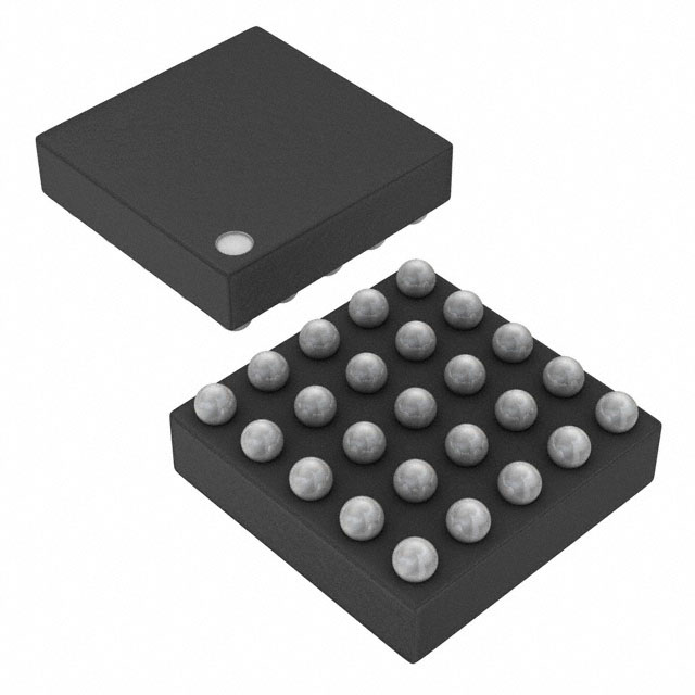


 工商网监
湘ICP备2023018690号
工商网监
湘ICP备2023018690号
