TLC5922
www.ti.com
SLVS486B – SEPTEMBER 2003 – REVISED OCTOBER 2009
LED DRIVER
Check for Samples: TLC5922
FEATURES
•
•
•
APPLICATIONS
1
2
•
•
•
•
•
•
•
•
•
•
16 Channels
Drive Capability
– 0 to 80 mA (Constant-Current Sink)
Constant Current Accuracy
– ±1% (typical)
Serial Data Interface, SPI Compatible
Fast Switching Output: Tr / Tf = 10ns (typical)
CMOS Level Input/Output
30 MHz Data Transfer Rate
VCC = 3.0 V to 5.5 V
Operating Temperature = –20°C to 85 °C
LED Supply Voltage up to 17 V
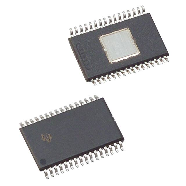
32-pin HTSSOP ( PowerPAD™) Package
Dot Correction
– 7 bit (128 Steps)
– Individually Adjustable For Each Channel
VCC
GND
PGND
SCLK
•
•
•
•
Controlled In-Rush Current
Monocolor, Multicolor, Fullcolor LED Display
Monocolor, Multicolor LED Signboard
Display Backlighting
Multicolor LED Lighting Applications
DESCRIPTION
The TLC5922 is a 16-channel constant-current sink
driver. Each channel has an On/Off state and a
128-step adjustable constant-current sink (dot
correction). The dot correction adjusts the brightness
variations between LED, LED channels, and other
LED drivers. Both dot correction and On/Off state are
accessible via a serial data interface. A single
external resistor sets the maximum current of all 16
channels.
SIN
MODE
XLAT
BLANK
Constant
Current
Driver
MODE
0
1
1
0
IREF
Maximum
OUTn Current
On/Off
Input
0
On/Off
Register
0
7−bit DC
Register
0
Shift
6
BLANK
Register
16
15
112
0
On/Off
Register
7−bit DC
Register
OUT0
Delay
x0
1
Constant
Current
Driver
OUT1
Delay
x1
7
13
DC Input
Shift
Register
BLANK
111
0
1
MODE
On/Off
Register
7−bit DC
Register
15
Constant
Current
Driver
OUT15
Delay
x15
105
111
SOUT
Figure 1. Functional Block Diagram
1
2
Please be aware that an important notice concerning availability, standard warranty, and use in critical applications of Texas
Instruments semiconductor products and disclaimers thereto appears at the end of this data sheet.
PowerPAD is a trademark of Texas Instruments.
PRODUCTION DATA information is current as of publication date.
Products conform to specifications per the terms of the Texas
Instruments standard warranty. Production processing does not
necessarily include testing of all parameters.
Copyright © 2003–2009, Texas Instruments Incorporated
�TLC5922
SLVS486B – SEPTEMBER 2003 – REVISED OCTOBER 2009
www.ti.com
This integrated circuit can be damaged by ESD. Texas Instruments recommends that all integrated circuits be handled with
appropriate precautions. Failure to observe proper handling and installation procedures can cause damage.
ESD damage can range from subtle performance degradation to complete device failure. Precision integrated circuits may be more
susceptible to damage because very small parametric changes could cause the device not to meet its published specifications.
ORDERING INFORMATION (1)
(1)
(2)
TA
Package
Part Number
–20 °C to 85 °C
4 mm x 4 mm, 32-pin HTSSOP
(2)
TLC5922DAP
For the most current package and ordering information, see the Package Option Addendum at the end
of this document, or see the TI website at www.ti.com.
The DAP package is available in tape and reel. Add R suffix (TLC5922DAPR) to order quantities of
2000 parts per reel.
ABSOLUTE MAXIMUM RATINGS
(1) (2)
TLC5922
UNIT
–0.3 to 6
V
90
mA
–0.3 to VCC + 0.3
V
VCC
Supply voltage (2)
IO
Output current (dc)
IL(LC)
VI
Input voltage range (2)
V(BLANK), V(XLAT), V(SCLK), V(SIN), V(MODE)
V(SOUT)
–0.3 to VCC + 0.3
V
–0.3 to 18
V
2
kV
500
V
–40 to 150
°C
VO
Output voltage range (2)
ESD rating
Tstg
(1)
(2)
V(OUT0) – V(OUT15)
HBM (JEDEC JESD22-A114, Human Body
Model)
CDM (JEDEC JESD22-C101, Charged Device
Model)
Storage temperature range
Continuous total power dissipation at (or below) TA = 25°C
3.9
W
Power dissipation rating at (or above) TA = 25°C
31.4
mW/°C
Stresses beyond those listed under Absolute Maximum Ratings may cause permanent damage to the device. These are stress ratings
only, and functional operation of the device at these or any other conditions beyond those indicated under Recommended Operating
Conditions is not implied. Exposure to absolute-maximum-rated conditions for extended periods may affect device reliability.
All voltage values are with respect to network ground terminal.
RECOMMENDED OPERATING CONDITIONS
DC Characteristics
MIN
VCC
Supply voltage
VO
Voltage applied to output, (Out0 - Out15)
VIH
High-level input voltage
VIL
Low-level input voltage
IOH
High-level output current
VCC = 5 V at SOUT
IOL
Low-level output current
VCC = 5 V at SOUT
IOLC
Constant output current
OUT0 to OUT15
TA
Operating free-air temperature range (1)
(1)
2
3
NOM
MAX
UNIT
5.5
V
17
V
0.8 VCC
VCC
V
GND
0.2 VCC
–20
V
–1
mA
1
mA
80
mA
85
°C
Contact TI sales for slightly extended temperature range.
Submit Documentation Feedback
Copyright © 2003–2009, Texas Instruments Incorporated
Product Folder Link(s): TLC5922
�TLC5922
www.ti.com
SLVS486B – SEPTEMBER 2003 – REVISED OCTOBER 2009
AC Characteristics
VCC = 3 V to 5.5 V, TA = –20°C to 85°C (unless otherwise noted)
MIN
TYP
MAX
UNIT
30
MHz
fSCLK
Clock frequency
SCLK
twh0/twl0
CLK pulse duration
SCLK = H/L
16
ns
twh1
XLAT pulse duration
XLAT = H
20
ns
tsu0
SIN – SCLK↑
10
ns
tsu1
SCLK↑ – XLAT↓
10
ns
Setup time
tsu2
MODE↑↓ – SCLK↑
10
ns
tsu3
MODE↑↓ – XLAT↓
10
ns
th0
SCLK↑ – SIN
10
ns
XLAT↓ – SCLK↑
10
ns
SCLK↑ – MODE↑↓
10
ns
XLAT↓ – MODE↑↓
10
ns
th1
Hold time
th2
th3
ELECTRICAL CHARACTERISTICS
VCC = 3 V to 5.5 V, TA = –20°C to 85°C (unless otherwise noted)
PARAMETER
TEST CONDITIONS
VOH
High-level output voltage
IOH = –1 mA, SOUT
VOL
Low-level output voltage
IOL = 1 mA, SOUT
II
Input current
VI = VCC or GND, BLANK, XLAT, SCLK, SIN, MODE
ICC
Supply current
MIN
TYP
MAX
VCC –0.5
UNIT
V
–1
0.5
V
1
µA
No data transfer, All output OFF, VO = 1 V,
R(IREF) = 10 kΩ
6
No data transfer, All output OFF, VO = 1 V,
R(IREF) = 1.3 kΩ
12
Data transfer 30 MHz, All output ON, VO = 1 V,
R(IREF) = 1.3 kΩ
25
mA
Data transfer 30 MHz, All output ON, VO = 1 V,
R(IREF) = 600 kΩ
36
65 (1)
80
90
mA
0.1
µA
Constant output current
All output ON, VO = 1 V, R(IREF) = 600 Ω
ILO0
Leakage output current
All output OFF, VO = 15 V, R(IREF) = 600 Ω , OUT0 to
OUT15
ΔIOLC0
Constant current error
All output ON, VO = 1 V, R(IREF) = 600 Ω, OUT0 to
OUT15
±1%
±4%
ΔIOLC1
Constant current error
device to device, averaged current from OUT0 to
OUT15, R(IREF) = 600 Ω
±4%
±8.5%
ΔIOLC2
Power supply rejection ratio
All output ON, VO = 1 V, R(IREF) = 600 Ω, OUT0 to
OUT15
±1
±4
%/V
ΔIOLC3
Load regulation
All output ON, VO = 1 V to 3 V, R(IREF) = 600 Ω,
OUT0 to OUT15
±2
±6
%/V
V(IREF)
Reference voltage output
R(IREF) = 600 Ω
1.24
1.28
IOLC
(1)
70
1.20
V
Measured at device start-up temperature. Once the IC is operating (self heating), lower ICC values are seen. See Figure 12 .
Submit Documentation Feedback
Copyright © 2003–2009, Texas Instruments Incorporated
Product Folder Link(s): TLC5922
3
�TLC5922
SLVS486B – SEPTEMBER 2003 – REVISED OCTOBER 2009
www.ti.com
SWITCHING CHARACTERISTICS
PARAMETER
tr0
TEST CONDITIONS
SOUT(see
Rise time
tr1
tf0
SOUT (see
tf1
(2)
)
10
(3)
MODE↑↓ – SOUT↑↓ (see
)
30
BLANK↓ – OUT0↑↓ (see
)
ns
ns
30
(4)
)
60
(4)
XLAT↑ – OUT0↑↓ (see
)
tpd4
XLAT↑ – IOUT(dot-correction) (see
OUTn↑↓ – OUT(n+1)↑↓ (see
30
UNIT
30
(3)
tpd3
(1)
(2)
(3)
(4)
(5)
10
16
tpd1
Output delay time
)
)
SCLK↑ – SOUT↑ ↓ (see
td
(2)
(1)
OUTx, VCC = 5 V, TA = 60°C, DCx = 7F (see
Propagation delay time
MAX
16
tpd0
tpd2
TYP
)
OUTx, VCC = 5 V, TA = 60°C, DCx = 7F (see
Fall time
MIN
(1)
ns
60
(5)
)
1000
(4)
)
14
22
30
ns
See Figure 4 . Defined as from 10% to 90%
See Figure 5 . Defined as from 10% to 90%
See Figure 4 . Figure 10
See Figure 5 and Figure 10
See Figure 5 and Figure 10
DAP PACKAGE
(TOP VIEW)
GND
BLANK
XLAT
SCLK
SIN
PGND
OUT0
OUT1
PGND
OUT2
OUT3
OUT4
OUT5
PGND
OUT6
OUT7
1
2
3
4
5
6
7
8
9
10
11
12
13
14
15
16
32
31
30
29
28
27
26
25
24
23
22
21
20
19
18
17
VCC
IREF
MODE
NC
SOUT
PGND
OUT15
OUT14
PGND
OUT13
OUT12
OUT11
OUT10
PGND
OUT9
OUT8
Terminal Functions
TERMINAL
NAME
NO.
BLANK
2
I/O
2
DESCRIPTION
Blank (Light OFF). When BLANK = H, All OUTx outputs are forced OFF. When BLANK = L,
ON/OFF of OUTx outputs are controlled by input data.
GND
1
IREF
31
I/O
MODE
30
I
Mode select. When MODE = L, SIN, SOUT, SCLK, XLAT are connected to ON/OFF control
logic. When MODE = H, SIN, SOUT, SCLK, XLAT are connected to dot-correction logic.
OUT0
7
O
Constant current output
OUT1
8
O
Constant current output
OUT2
10
O
Constant current output
OUT3
11
O
Constant current output
OUT4
12
O
Constant current output
OUT5
13
O
Constant current output
4
Ground
Reference current terminal
Submit Documentation Feedback
Copyright © 2003–2009, Texas Instruments Incorporated
Product Folder Link(s): TLC5922
�TLC5922
www.ti.com
SLVS486B – SEPTEMBER 2003 – REVISED OCTOBER 2009
Terminal Functions (continued)
TERMINAL
I/O
DESCRIPTION
15
O
Constant current output
16
O
Constant current output
OUT8
17
O
Constant current output
OUT9
18
O
Constant current output
OUT10
20
O
Constant current output
OUT11
21
O
Constant current output
OUT12
22
O
Constant current output
OUT13
23
O
Constant current output
OUT14
25
O
Constant current output
OUT15
26
O
Constant current output
PGND
6, 14, 19, 24,
27
SCLK
4
NAME
NO.
OUT6
OUT7
Power ground
I
Data shift clock. Note that the internal connections are switched by MODE (pin #30). At
SCLK↑, the shift-registers selected by MODE shift the data.
SIN
5
I
Data input of serial I/F
SOUT
28
O
Data output of serial I/F
VCC
32
NC
29
–
Not Connected
XLAT
3
I
Data latch. Note that the internal connections are switched by MODE (pin #30). At XLAT↑, the
latches selected by MODE get new data.
Power supply voltage
PIN EQUIVALENT INPUT AND OUTPUT SCHEMATIC DIAGRAMS
(Note: Resistor values are equivalent resistance and not tested).
VCC
INPUT
400 W
GND
Figure 2. Input Equivalent Circuit (BLANK, XLAT, SCLK, SIN, MODE)
10 W
SOUT
GND
Figure 3. Output Equivalent Circuit
Submit Documentation Feedback
Copyright © 2003–2009, Texas Instruments Incorporated
Product Folder Link(s): TLC5922
5
�TLC5922
SLVS486B – SEPTEMBER 2003 – REVISED OCTOBER 2009
www.ti.com
PARAMETER MEASUREMENT INFORMATION
SOUT
15 pF
Figure 4. Test Circuit for tr0, tf0, td0, td1
51 Ω
OUTn
15 pF
Figure 5. Test Circuit for tr1, tf1, tpd2, tpd3, tpd4
6
Submit Documentation Feedback
Copyright © 2003–2009, Texas Instruments Incorporated
Product Folder Link(s): TLC5922
�TLC5922
www.ti.com
SLVS486B – SEPTEMBER 2003 – REVISED OCTOBER 2009
PRINCIPLES OF OPERATION
Setting Maximum Channel Current
The maximum output current per channel is set by a single external resistor, R(IREF), which is placed between
IREF and GND. The voltage on IREF is set by an internal band gap V(IREF) with a typical value of 1.24V. The
maximum channel current is equivalent to the current flowing through R(IREF) multiplied by a factor of 40. The
maximum output current can be calculated by Equation 1:
V
I
+ IREF
40
MAX
R
IREF
(1)
where:
VIREF = 1.24V typ.
RIREF = User selected external resistor (RIREF should not be smaller than 600 Ω)
Figure 6 shows the maximum output current, IO(LC), versus R(IREF) . In Figure 6, R(IREF) is the value of the resistor
between IREF terminal to ground, and IO(LC) is the constant output current of OUT0,.....OUT15.
100 k
48.8 k
10 k
9.76 k
4.88 k
2.44 k
1.63 k
1.22 k
976
1k
IREF
− Reference Resistor −
Ω
VOutn = 1 V
DC = 127
813
R
697
100
0
0.01
0.02
0.03
0.04
0.05
0.06
0.07 0.08
IOLC − Output Current − mA
Figure 6. Reference Resistor vs Output Current
Setting Dot-Correction
The TLC5922 has the capability to fine adjust the current of each channel, OUT0 to OUT15 independently. This
is also called dot correction. This feature is used to adjust the brightness deviations of LED connected to the
output channels OUT0 to OUT15. Each of the 16 channels can be programmed with a 7-bit word. The channel
output can be adjusted in 128 steps from 0% to 100% of the maximum output current IMAX. Equation 2
determines the output current for each OUTn:
I
DCn
I
+ MAX
Outn
127
(2)
where:
IMax = the maximum programmable current of each output
DCn = the programmed dot-correction value for output n (DCn = 0, 1, 2 ...127)
n = 0, 1, 2 ... 15
Submit Documentation Feedback
Copyright © 2003–2009, Texas Instruments Incorporated
Product Folder Link(s): TLC5922
7
�TLC5922
SLVS486B – SEPTEMBER 2003 – REVISED OCTOBER 2009
www.ti.com
Dot-correction data are entered for all channels at the same time. The complete dot-correction data format
consists of 16 x 7-bit words, which forms a 112-bit wide serial data packet. The channel data is put one after
another. All data is clocked in with MSB first. Figure 7 shows the DC data format.
LSB
MSB
0
6
7
104
105
111
DC 0.0
DC 0.6
DC 1.0
DC 14.6
DC 15.0
DC 15.6
DC OUT0
DC OUT15
DC OUT2 − DC OUT14
Figure 7. DC Data Format
MODE must be set to high to input data into the dot-correction register. The internal input shift register is then set
to 112-bit width. After all serial data is clocked in, a rising edge of XLAT latches the data to the dot-correction
register (Figure 10).
Output Enable
All OUTn channels of TLC5922 can switched off with one signal. When BLANK signal is set to high, all OUTn are
disabled, regardless of On/Off status of each OUTn. When BLANK is set to low, all OUTn work under normal
conditions.
Table 1. BLANK Signal Truth Table
BLANK
OUT0 - OUT15
LOW
Normal condition
HIGH
Disabled
Setting Channel On/Off Status
All OUTn channels of TLC5922 can be switched on or off independently. Each of the channels can be
programmed with a 1-bit word. On/Off data are entered for all channels at the same time. The complete On/Off
data format consists of 16 x 1-bit words, which form a 16-bit wide data packet. The channel data is put one after
another. All data is clocked in with MSB first. Figure 8 shows the On/Off data format.
LSB
0
MSB
15
On/Off
OUT0
On/Off
OUT1
On/Off
OUT2
On/Off
OUT3
On/Off
OUT4
On/Off
OUT5
On/Off
OUT6
On/Off
OUT7
On/Off
OUT8
On/Off
OUT9
On/Off
OUT10
On/Off
OUT11
On/Off
OUT12
On/Off
OUT13
On/Off
OUT14
On/Off
OUT15
On/Off Data
Figure 8. On/Off Data
MODE must be set to low to input On/Off data into the On/Off register. The internal input shift register is then set
to 16-bit width. After all serial data is clocked in, a rising edge of XLAT, during BLANK = high, is used to latch
data into the On/Off register. Figure 10 shows the On/Off data input timing chart.
Delay Between Outputs
The TLC5922 has graduated delay circuits between outputs. These delay circuits can be found in the constant
current block of the device (see Figure 1). The fixed delay time is 20 ns (typical), OUT0 has no delay, OUT1 has
20-ns delay, OUT2 has 40-ns delay, etc. This delay prevents large inrush currents, which reduce power supply
bypass capacitor requirements when the outputs turn on.
8
Submit Documentation Feedback
Copyright © 2003–2009, Texas Instruments Incorporated
Product Folder Link(s): TLC5922
�TLC5922
www.ti.com
SLVS486B – SEPTEMBER 2003 – REVISED OCTOBER 2009
Serial Interface Data Transfer Rate
The TLC5922 includes a flexible serial interface, which can be connected to a microcontroller or digital signal
processor. Only 3 pins are required to input data into the device. The rising edge of SCLK signal shifts the data
from SIN pin to internal shift register. After all data is clocked in, a rising edge of XLAT latches the serial data to
the internal registers. All data is clocked in with MSB first. Multiple TLC5922 devices can be cascaded by
connecting SOUT pin of one device to the SIN pin of following device.
V LED
V LED
OUT0
SIN
Controller
OUT15
SOUT
V CC
SIN
SCLK
XLAT
MODE
SCLK
XLAT
MODE
BLANK
BLANK
VLED
100 nF
TLC5922
IREF
V LED
OUT0
SCLK
XLAT
MODE
SOUT
VCC
TLC5922
BLANK
IC 0
SOUT
OUT15
SIN
100 nF
IREF
IC n
4
Figure 9. Cascading Devices
Figure 9 shows an example application with n cascaded TLC5922 devices connected to a controller. The
maximum number of cascaded TLC5922 devices depends on the application system, and data transfer rate.
Equation 3 calculates the minimum data input frequency needed.
f_(SCLK) + 112
f_(update)
n
(3)
where:
f_(SCLK): The minimum data input frequency for SCLK and SIN.
f_(update): The update rate of the whole cascaded system.
n: The number of cascaded TLC5922 devices.
Operating Modes
The TLC5922 has different operating modes, depending on the MODE signal. Table 2 shows the available
operating modes.
Table 2. TLC5922 Operating Modes Truth Table
MODE SIGNAL
INPUT SHIFT REGISTER
MODE
LOW
16 bit
On/Off Mode
HIGH
112 bit
Dot-Correction Data Input Mode
Submit Documentation Feedback
Copyright © 2003–2009, Texas Instruments Incorporated
Product Folder Link(s): TLC5922
9
�10
Submit Documentation Feedback
Product Folder Link(s): TLC5922
OUT1
OUT0
BLANK
SOUT
SCLK
SIN
XLAT
MODE
t pd3
On/Off
MSB
On/Off
LSB
t wh1
t h3
tpd 2
On/Off Mode Data
Input Cycle
tpd 1
td
t pd 2
DC
MSB
twh0
DC
MSB
tsu 3
DC
LSB
f CLK
t wl 0
DC Mode Data Input
Cycle
t pd 4
tsu 0
DC
LSB
DC
MSB
t pd0
t h1
DC
MSB
t h0
DC
LSB
t su1
t h2
DC
MSB
DC
LSB
t h3
DC Mode Data Input
Cycle
t pd 4
On/Off
MSB
t pd1
t su2
On/Off
MSB
t su 3
On/Off
LSB
On/Off
MSB
On/Off
LSB
On/Off Mode Data
Input Cycle
On/Off
MSB−1
On/Off
MSB
On/Off
MSB
On/Off Mode Data
Input Cycle
TLC5922
SLVS486B – SEPTEMBER 2003 – REVISED OCTOBER 2009
www.ti.com
Figure 10. Timing Chart Example for ON/OFF Setting to Dot-Correction
Copyright © 2003–2009, Texas Instruments Incorporated
�TLC5922
www.ti.com
SLVS486B – SEPTEMBER 2003 – REVISED OCTOBER 2009
Power Rating - Free-Air Temperature
Figure 11 shows total power dissipation. Figure 12 shows supply current versus free-air temperature.
3.9
3.2
1.48
2
−20
0
VO − Output Voltage − V
PD − Power Dissipation − W
Power Dissipation
vs
Temperature
25
85
TA − Free-Air Temperature − °C
Figure 11.
Supply Current
vs
Free-Air Temperature
70
ICC − Supply Current − mA
60
50
40
30
20
10
0
−50 −30 −10 10
30
50
70
90
110 130 150
TA − Free-Air Temperature − °C
Data Transfer = 30 MHz / All Outputs, ON/VO = 1 V / RIREF = 600 Ω / AVDD = 5 V
Figure 12.
Submit Documentation Feedback
Copyright © 2003–2009, Texas Instruments Incorporated
Product Folder Link(s): TLC5922
11
�TLC5922
SLVS486B – SEPTEMBER 2003 – REVISED OCTOBER 2009
www.ti.com
REVISION HISTORY
NOTE: Page numbers of current version may differ from previous versions.
Changes from Revision A (March 2005) to Revision B
•
12
Page
Changed Propogation delay time tPD0 and tPD1 from 300 ns MAX(typographical error) to 30 ns MAX ................................ 4
Submit Documentation Feedback
Copyright © 2003–2009, Texas Instruments Incorporated
Product Folder Link(s): TLC5922
�Thermal Pad Mechanical Data
www.ti.com
DAP (R–PDSO–G32)
THERMAL INFORMATION
The DAP PowerPAD™ package incorporates an exposed thermal die pad that is designed to be attached directly
to an external heat sink. When the thermal die pad is soldered directly to the printed circuit board (PCB), the PCB
can be used as a heatsink. In addition, through the use of thermal vias, the thermal die pad can be attached directly
to a ground plane or special heat sink structure designed into the PCB. This design optimizes the heat transfer from
the integrated circuit (IC).
For additional information on the PowerPAD package and how to take advantage of its heat dissipating abilities, refer to
Technical Brief, PowerPAD Thermally Enhanced Package, Texas Instruments Literature No. SLMA002 and
Application Brief, PowerPAD Made Easy, Texas Instruments Literature No. SLMA004. Both documents are available
at www.ti.com. See Figure 1 for DAP package exposed thermal die pad dimensions.
32
1
Exposed Thermal
Die Pad
3,91
3,31
17
16
4,11
3,35
Bottom View
PPTD001
NOTE: All linear dimensions are in millimeters.
Figure 1. DAP Package Exposed Thermal Die Pad Dimensions
PowerPAD is a trademark of Texas Instruments.
1
�PACKAGE OPTION ADDENDUM
www.ti.com
13-Aug-2021
PACKAGING INFORMATION
Orderable Device
Status
(1)
Package Type Package Pins Package
Drawing
Qty
Eco Plan
(2)
Lead finish/
Ball material
MSL Peak Temp
Op Temp (°C)
Device Marking
(3)
(4/5)
(6)
TLC5922DAP
ACTIVE
HTSSOP
DAP
32
46
RoHS & Green
NIPDAU
Level-3-260C-168 HR
-20 to 85
TLC5922
TLC5922DAPG4
ACTIVE
HTSSOP
DAP
32
46
RoHS & Green
NIPDAU
Level-3-260C-168 HR
-20 to 85
TLC5922
TLC5922DAPR
ACTIVE
HTSSOP
DAP
32
2000
RoHS & Green
NIPDAU
Level-3-260C-168 HR
-20 to 85
TLC5922
TLC5922DAPRG4
ACTIVE
HTSSOP
DAP
32
2000
RoHS & Green
NIPDAU
Level-3-260C-168 HR
-20 to 85
TLC5922
(1)
The marketing status values are defined as follows:
ACTIVE: Product device recommended for new designs.
LIFEBUY: TI has announced that the device will be discontinued, and a lifetime-buy period is in effect.
NRND: Not recommended for new designs. Device is in production to support existing customers, but TI does not recommend using this part in a new design.
PREVIEW: Device has been announced but is not in production. Samples may or may not be available.
OBSOLETE: TI has discontinued the production of the device.
(2)
RoHS: TI defines "RoHS" to mean semiconductor products that are compliant with the current EU RoHS requirements for all 10 RoHS substances, including the requirement that RoHS substance
do not exceed 0.1% by weight in homogeneous materials. Where designed to be soldered at high temperatures, "RoHS" products are suitable for use in specified lead-free processes. TI may
reference these types of products as "Pb-Free".
RoHS Exempt: TI defines "RoHS Exempt" to mean products that contain lead but are compliant with EU RoHS pursuant to a specific EU RoHS exemption.
Green: TI defines "Green" to mean the content of Chlorine (Cl) and Bromine (Br) based flame retardants meet JS709B low halogen requirements of


 工商网监
湘ICP备2023018690号
工商网监
湘ICP备2023018690号
