TPA2000D2
www.ti.com
SLOS291F – MARCH 2000 – REVISED MARCH 2007
2-W FILTERLESS STEREO CLASS-D AUDIO POWER AMPLIFIER
•
FEATURES
•
•
•
•
•
Modulation Scheme Optimized to Operate
Without a Filter
2 W Into 3-Ω Speakers (THD+N< 0.4%)
< 0.08% THD+N at 1 W, 1 kHz, Into 4-Ω Load
Extremely Efficient Third Generation 5-V
Class-D Technology:
– Low Supply Current (No Filter) . . . 8 mA
– Low Supply Current (Filter) . . . 15 mA
– Low Shutdown Current . . . 1 µA
– Low Noise Floor . . . 56 µVRMS
– Maximum Efficiency Into 3 Ω, 65-70%
– Maximum Efficiency Into 8 Ω, 75-85%
– 4 Internal Gain Settings . . . 8-23.5 dB
– PSRR . . . -77 dB
Integrated Depop Circuitry
•
Short-Circuit Protection (Short to Battery,
Ground, and Load)
-40°C to 85°C Operating Temperature Range
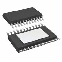
PW OR PWP PACKAGE
(TOP VIEW)
PGND
LOUTN
GAIN0
PVDD
LINN
AGND
COSC
RINN
PVDD
SHUTDOWN
ROUTN
PGND
1
2
3
4
5
6
7
8
9
10
11
12
24
23
22
21
20
19
18
17
16
15
14
13
PGND
LOUTP
BYPASS
PVDD
LINP
VDD
ROSC
RINP
PVDD
GAIN1
ROUTP
PGND
DESCRIPTION
The TPA2000D2 is the third generation 5-V class-D amplifier from Texas Instruments. Improvements to previous
generation devices include: lower supply current, lower noise floor, better efficiency, four different gain settings,
smaller packaging, and fewer external components. The most significant advancement with this device is its
modulation scheme that allows the amplifier to operate without the output filter. Eliminating the output filter saves
the user approximately 30% in system cost and 75% in PCB area.
The TPA2000D2 is a monolithic class-D power IC stereo audio amplifier, using the high switching speed of
power MOSFET transistors. These transistors reproduce the analog signal through high-frequency switching of
the output stage. The TPA2000D2 is configured as a bridge-tied load (BTL) amplifier capable of delivering
greater than 2 W of continuous average power into a 3-Ω load at less than 1% THD+N from a 5-V power supply
in the high fidelity range (20 Hz to 20 kHz). With 1 W being delivered to a 4-Ω load at 1 kHz, the typical THD+N
is less than 0.08%.
A BTL configuration eliminates the need for external coupling capacitors on the output. Low supply current of 8
mA makes the device ideal for battery-powered applications. Protection circuitry increases device reliability:
thermal, over-current, and under-voltage shutdown.
Efficient class-D modulation enables the TPA2000D2 to operate at full power into 3-Ω loads at an ambient
temperature of 85°C.
AVAILABLE OPTIONS (1)
TA
–40°C to 85°C
(1)
(2)
PACKAGED DEVICE
TSSOP (PW)
TSSOP (PWP) (2)
TPA2000D2PW
TPA2000D2PWP
For the most current package and ordering information, see the Package Option Addendum at the end
of this document, or see the TI web site at www.ti.com.
The PWP package is available taped and reeled. To order a taped and reeled part, add the suffix R to
the part number (e.g., TPA2000D2PWPR).
Please be aware that an important notice concerning availability, standard warranty, and use in critical applications of Texas
Instruments semiconductor products and disclaimers thereto appears at the end of this data sheet.
PRODUCTION DATA information is current as of publication date.
Products conform to specifications per the terms of the Texas
Instruments standard warranty. Production processing does not
necessarily include testing of all parameters.
Copyright © 2000–2007, Texas Instruments Incorporated
�TPA2000D2
www.ti.com
SLOS291F – MARCH 2000 – REVISED MARCH 2007
These devices have limited built-in ESD protection. The leads should be shorted together or the device placed in conductive foam
during storage or handling to prevent electrostatic damage to the MOS gates.
VDD
AGND
PVDD
VDD
Gain
Adjust
RINN
+
_
Gate
Drive
ROUTN
_
+
PGND
+
_
PVDD
_
Gain
Adjust
RINP
Gate
Drive
+
ROUTP
PGND
SHUTDOWN
2
GAIN1
GAIN0
Gain
Biases
and
References
Start-Up
Protection
Logic
Ramp
Generator
COSC
ROSC
BYPASS
Thermal
OC
Detect
OC
Detect
VDD ok
PVDD
LINP
Gain
Adjust
+
_
Gate
Drive
_
+
PGND
+
_
PVDD
_
LINN
LOUTP
Gain
Adjust
+
Gate
Drive
LOUTN
PGND
2
Submit Documentation Feedback
�TPA2000D2
www.ti.com
SLOS291F – MARCH 2000 – REVISED MARCH 2007
TERMINAL FUNCTION
TERMINAL
NAME
NO.
I/O
DESCRIPTION
AGND
6
-
Analog ground
BYPASS
22
I
Tap to voltage divider for internal midsupply bias generator used for analog reference.
COSC
7
I
A capacitor connected to this terminal sets the oscillation frequency in conjunction with ROSC. For
proper operation, connect a 220 pF capacitor from COSC to ground.
GAIN0
3
I
Bit 0 of gain control (TTL logic level)
GAIN1
15
I
Bit 1 of gain control (TTL logic level)
LINN
5
I
Left channel negative differential audio input
LINP
20
I
Left channel positive differential audio input
LOUTN
2
O
Left channel negative audio output
LOUTP
23
O
Left channel positive audio output
PGND
PVDD
1, 24
-
Power ground for left channel H-bridge
12, 13
-
Power ground for right channel H-bridge
4, 21
-
Power supply for left channel H-bridge
9, 16
-
Power supply for right channel H-bridge
RINN
8
I
Right channel negative differential audio input
RINP
17
I
Right channel positive differential audio input
ROSC
18
I
A resistor connected to this terminal sets the oscillation frequency in conjunction with COSC. For
proper operation, connect a 120 kΩ resistor from ROSC to ground.
ROUTN
11
O
Right channel negative audio output
ROUTP
14
O
Right channel positive output
SHUTDOWN
10
I
Places the amplifier in shutdown mode if a TTL logic low is placed on this terminal; normal operation if
a TTL logic high is placed on this terminal.
VDD
19
-
Analog power supply
ABSOLUTE MAXIMUM RATINGS
over operating free-air temperature range (unless otherwise noted) (1)
UNIT
VDD, PVDD
Supply voltage
VI
Input voltage
-0.3 V to 6 V
-0.3 V to VDD+0.3 V
Continuous total power dissipation
See Dissipation Rating Table
TA
Operating free-air temperature range
-40°C to 85°C
TJ
Operating junction temperature range
-40°C to 150°C
Tstg
Storage temperature range
-65°C to 150°C
Lead temperature 1,6 mm (1/16 inch) from case for 10 seconds
(1)
260°C
Stresses beyond those listed under absolute maximum ratings may cause permanent damage to the device. These are stress ratings
only, and functional operation of the device at these or any other conditions beyond those indicated under recommended operating
conditions is not implied. Exposure to absolute-maximum-rated conditions for extended periods may affect device reliability.
DISSIPATION RATING TABLE
PACKAGE
TA ≤ 25°C
POWER RATING
DERATING FACTOR
ABOVE TA = 25°C
TA = 70°C
POWER RATING
TA = 85°C
POWER RATING
PW
1.04 W
8.34 mW/°C
0.67 W
0.54 W
PWP
2.7 W
21.8 mW/°C
1.7 W
1.4 W
Submit Documentation Feedback
3
�TPA2000D2
www.ti.com
SLOS291F – MARCH 2000 – REVISED MARCH 2007
RECOMMENDED OPERATING CONDITIONS
MIN
TYP MAX
4.5
5.5
UNIT
VDD, PVDD
Supply voltage
VIH
High-level input voltage
GAIN0, GAIN1, SHUTDOWN
VIL
Low-level input voltage
GAIN0, GAIN1, SHUTDOWN
ROSC
Oscillator resistance
120
COSC
Oscillator capacitance
220
fs
Switching frequency
200
300
kHz
TA
Operating free-air temperature
-40
85
°C
2
V
V
0.8
V
kΩ
pF
ELECTRICAL CHARACTERISTICS
TA = 25°C, VDD = PVDD = 5 V (unless otherwise noted)
PARAMETER
TEST CONDITIONS
MIN
| VOO |
Output offset voltage (measured differentially)
VI = 0 V
PSRR
Power supply rejection ratio
VDD=PVDD = 4.5 V to 5.5 V
IIH
High-level input current
VDD=PVDD = 5.5 V, VI = VDD = PVDD
IIL
Low-level input current
VDD=PVDD = 5.5 V, VI = 0 V
IDD
Supply current
No filter (with or without speaker load)
IDD
Supply current
With filter, L = 22 µH, C = 1 µF
IDD(SD)
Supply current, shutdown mode
TYP
MAX
25
mV
1
µA
-77
8
UNIT
dB
1
µA
10
mA
15
mA
1
15
TYP
MAX
µA
OPERATING CHARACTERISTICS
TA = 25°C, VDD = PVDD = 5 V, RL = 4 Ω, Gain = 8 dB (unless otherwise noted)
PARAMETER
TEST CONDITIONS
PO
Output power
THD = 0.1%, f = 1 kHz, RL = 3 Ω
THD+N
Total harmonic distortion plus noise
PO = 1 W, f = 20 Hz to 20 kHz
BOM
Maximum output power bandwidth
THD = 5%
kSVR
Supply ripple rejection ratio
f = 1 kHz, C(BYPASS) = 0.4 µF
SNR
Signal-to-noise ratio
Integrated noise floor
ZI
MIN
2
20
20 Hz to 20 kHz, No input
dB
87
dBV
56
µV
>20
kΩ
4
AMPLIFIER GAIN
(dB)
INPUT IMPEDANCE
(kΩ)
TYP
TYP
0
0
8
104
0
1
12
74
1
0
17.5
44
1
1
23.5
24
Submit Documentation Feedback
kHz
-60
Table 1. Gain Settings
GAIN0
W


 工商网监
湘ICP备2023018690号
工商网监
湘ICP备2023018690号
