TPA2051D3
www.ti.com ..................................................................................................................................................... SLOS641A – JUNE 2009 – REVISED OCTOBER 2009
2.9 W/Channel Mono Class-D Audio Subsystem with DirectPath™ Headphone Amplifier &
SpeakerGuard™
FEATURES
1
• Mono Class-D Amp: 730 mW into 8 Ω from 3.6
V Supply (1% THD)
• Class-D Bypass Switches
• DirectPath™ Stereo Headphone Amplifier
– No Output Capacitors Required
• SpeakerGuard™ Automatic Gain Control
(AGC)
• One Differential Mono and Two Stereo
Single-Ended Inputs
• 3:1 Input MUX with Mode Control
• 32-Step Volume Control for Both Input
Channels
• Independent Volume Controls for All Inputs
• Independent Shutdown for Headphone and
Class-D Amplifiers
• I2C™ Interface
• Short-Circuit and Thermal-Overload Protection
• Operates from 2.5 V to 5.5 V
• 25-Ball 2,16 mm × 2,11 mm, 0,4 mm pitch
WCSP
23
APPLICATIONS
•
•
•
•
Smart Phones / Cellular Phones
Portable Media Players
Portable Gaming
Multimedia Platforms
DESCRIPTION
The TPA2051D3 is an audio subsystem with a mono
Class-D power amplifier, a stereo DirectPath
headphone amplifier, and bypass switches. The
DirectPath headphone amplifier eliminates the need
for external dc-blocking output capacitors. The built-in
charge pump creates a negative supply voltage for
the headphone amplifier, allowing a 0 V dc bias at the
output. The DirectPath headphone amplifier drives
25 mW into 16 Ω speakers from a 4.2 V supply.
The subsystem includes three inputs: A differential
mono input and two stereo single-ended (SE) inputs.
The stereo inputs are also configurable as differential
mono inputs. Each input channel has an independent
volume control. Seven operating modes provide
input-to-output combinations and shutdown control.
Operating mode and volume levels are controlled
over a 1.8 V compatible I2C interface.
The TPA2051D3 uses SpeakerGuardTM technology to
prevent output clipping distortion and excessive
power to the speaker and headphones.
The Class-D amplifier includes a bypass mode. This
allows the baseband IC (BB) to directly drive the 8Ω
speaker. This is useful for dual-mode speaker phones
in voice–only mode.
The Class-D amplifier uses 4.9 mA and the
DirectPath amplifier uses 4.1 mA of typical quiescent
current. Total supply current reduces to less than
1 µA in shutdown.
The TPA2051D3 is available in a 25-bump 2,16 mm
× 2,11 mm, 0,4 mm pitch WCSP with less than
0.8 mm height.
Bypass+
BypassMono+
ABB
Mono-
Left
(SE)
TPA2051D3
Mono Class-D
plus
DirectPathTM
8 Dual-Mode
Speaker
Codec
(MP3)
Right
(SE)
Left
(SE)
Stereo
Headphone Jack
FM Tuner
Right
(SE)
1
2
3
Please be aware that an important notice concerning availability, standard warranty, and use in critical applications of Texas
Instruments semiconductor products and disclaimers thereto appears at the end of this data sheet.
DirectPath, SpeakerGuard are trademarks of Texas Instruments.
I2C is a trademark of NXP B.V. Corporation, Netherlands.
PRODUCTION DATA information is current as of publication date.
Products conform to specifications per the terms of the Texas
Instruments standard warranty. Production processing does not
necessarily include testing of all parameters.
Copyright © 2009, Texas Instruments Incorporated
�TPA2051D3
SLOS641A – JUNE 2009 – REVISED OCTOBER 2009 ..................................................................................................................................................... www.ti.com
These devices have limited built-in ESD protection. The leads should be shorted together or the device placed in conductive foam
during storage or handling to prevent electrostatic damage to the MOS gates.
FUNCTIONAL BLOCK DIAGRAM
PVDD
1 mF
BYPASS+
MONO+
MONO-
Voice- Mode
Bypass
+
–
PVDD
Gain
Select:
-60 dB to +18 dB
Volume Control
PWM
+12 dB
+6 dB
HBridge
OUT+
OUT-
PGND
BYPASSVoice - Mode
Bypass
INL1
Mux
+
Mode
Control
+
-60 dB to +18 dB
Volume Control
INR1
SpeakerGuard ™
AGC
INL2
-60 dB to +18 dB
Volume Control
HPVDD
Gain
Select:
0 dB
to
-12 dB
HPL
HPVSS
HPVDD
1.5 dB/
step
INR2
HPR
HPVSS
DVDD
SDA
I2C Interface
SCL
CPP
Bias Control
and Pop
Suppression
EN
VREF
1 mF
AGND
Charge
Pump
1 mF
CPN
HPVDD
2.2 mF
HPVSS
PGND
2.2 mF
AVDD
2
Submit Documentation Feedback
Copyright © 2009, Texas Instruments Incorporated
Product Folder Link(s): TPA2051D3
�TPA2051D3
www.ti.com ..................................................................................................................................................... SLOS641A – JUNE 2009 – REVISED OCTOBER 2009
DEVICE PINOUT
A1
A2
A3
A4
A5
OUT+
PVDD
PGND
OUT–
CPN
B1
B2
B3
B4
B5
AVDD
BYPASS+
BYPASS–
DVDD
CPP
C1
C2
C3
C4
C5
MONO–
SDA
SCL
EN
HPL
D1
D2
D3
D4
D5
MONO+
INL2
INL1
HPVDD
HPVSS
E1
E2
E3
E4
E5
INR2
INR1
VREF
AGND
HPR
Submit Documentation Feedback
Copyright © 2009, Texas Instruments Incorporated
Product Folder Link(s): TPA2051D3
3
�TPA2051D3
SLOS641A – JUNE 2009 – REVISED OCTOBER 2009 ..................................................................................................................................................... www.ti.com
PIN FUNCTIONS
PIN
INPUT/ OUTPUT/
POWER
(I/O/P)
DESCRIPTION
NAME
BALL
WCSP
OUT+
A1
O
Speaker positive output; connect to + terminal of loudspeaker
PVDD
A2
P
Supply for Class-D amplifier. Connect to voltage supply
PGND
A3
P
Ground for Class-D amplifier; connect to GND directly or to the ground
plane
OUT–
A4
O
Speaker negative output; connect to – terminal of loudspeaker
CPN
A5
P
Charge pump flying capacitor negative terminal. Connect negative side of
capacitor between CPP and CPN
AVDD
B1
P
Connect to voltage supply
BYPASS+
B2
I
Bypass Mode positive input
BYPASS–
B3
I
Bypass Mode negative input
DVDD
B4
P
Connect to I2C bus supply voltage
CPP
B5
P
Charge pump flying capacitor positive terminal. Connect positive side of
capacitor between CPP and CPN
MONO–
C1
I
Mono negative differential input
SDA
C2
I/O
I2C data input
SCL
C3
I
I2C clock input
EN
C4
I
Master shutdown
HPL
C5
O
Headphone left channel output
MONO+
D1
I
Mono positive differential input
INL2
D2
I
Input channel 2 left input
INL1
D3
I
Input channel 1 left input
HPVDD
D4
O
Headphone reference voltage. Connect to 2.2 µF capacitor to ground
HPVSS
D5
P
Negative supply generated by the charge pump. Connect a 2.2 µF cap to
ground to reduce voltage ripple
INR2
E1
I
Input channel 2 right input
INR1
E2
I
Input channel 1 right input
VREF
E3
I
Reference voltage. Connect to 1 µF capacitor to ground
AGND
E4
P
Connect to ground plane
HPR
E5
O
Headphone right channel output
ORDERING INFORMATION
TA
PACKAGED DEVICES (1)
–40°C to 85°C
(1)
(2)
4
25-ball WSCP
PART NUMBER (2)
SYMBOL
TPA2051D3YFFR
TPA2051
TPA2051D3YFFT
TPA2051
For the most current package and ordering information, see the Package Option Addendum at the end of this document, or see the TI
Web site at www.ti.com.
The YFF package is only available taped and reeled. The suffix “R” indicates a reel of 3000, the suffix “T” indicates a reel of 250.
Submit Documentation Feedback
Copyright © 2009, Texas Instruments Incorporated
Product Folder Link(s): TPA2051D3
�TPA2051D3
www.ti.com ..................................................................................................................................................... SLOS641A – JUNE 2009 – REVISED OCTOBER 2009
ABSOLUTE MAXIMUM RATINGS
over operating free-air temperature range, TA = 25°C (unless otherwise noted)
VALUE / UNIT
Supply voltage, AVDD, PVDD
–0.3 V to 6.0 V
I2C Supply Voltage DVDD
VI
–0.3 to 3.6 V
Input Voltage
–0.3 V to AVDD + 0.3 V
Output Continuous total power dissipation
See Dissipation Rating Table
TA
Operating free-air temperature range
–40°C to 85°C
TJ
Operating junction temperature range
–40°C to 150°C
Tstg
Storage temperature range
–65°C to 85°C
DISSIPATION RATINGS
PACKAGE
TA < 25°C
POWER RATING
OPERATING FACTOR
ABOVE TA = 25°C
TA = 70°C
POWER RATING
TA = 85°C
POWER RATING
YFF (WCSP)
845 mW
6.757 mW/°C
540 mW
440 mW
RECOMMENDED OPERATING CONDITIONS
MIN
MAX
Supply voltage, AVDD, PVDD
2.5
5.5
V
I2C supply voltage, DVDD
1.7
3.3
V
VIH
High-level input voltage
VIL
Low-level input voltage
TA
SDA, SCL, EN, DVDD = 1.8 V
1.3
SDA, SCL, EN, DVDD = 3.3 V
3.0
UNIT
V
V
SDA, SCL, EN, DVDD = 1.8 V
0.3
V
SDA, SCL, EN, DVDD = 3.3 V
0.3
V
85
°C
MAX
UNIT
Operating free-air temperature
–40
ELECTRICAL CHARACTERISTICS
over operating free-air temperature range, TA = 25°C (unless otherwise noted)
MIN
TYP
Power supply rejection ratio (Class-D amplifier)
PARAMETER
AVDD = PVDD = 2.5 V to 5.5 V, Single-ended
modes
TEST CONDITIONS
60
75
dB
Power supply rejection ratio (headphone
amplifiers)
AVDD = PVDD = 2.5 V to 5.5 V, Single-ended
modes
75
85
dB
High-level input current (SDA, SCL, EN)
1
µA
Low-level input current (SDA, SCL, EN)
1
µA
Supply current
AVDD = PVDD = 2.5 V, Class-D and headphone
amplifiers active, no load
6.3
7.5
mA
AVDD = PVDD = 3.6 V, Class-D and headphone
amplifiers active, no load
7.1
8.5
mA
AVDD = PVDD = 3.6 V, headphone active,
Class-D deactivated, no load
4.1
5.25
mA
AVDD = PVDD = 3.6 V, Class-D active,
headphone deactivated, no load
4.9
6.0
mA
AVDD = PVDD = 2.5 V to 5.5 V, Full shutdown
mode
0.2
1
µA
Submit Documentation Feedback
Copyright © 2009, Texas Instruments Incorporated
Product Folder Link(s): TPA2051D3
5
�TPA2051D3
SLOS641A – JUNE 2009 – REVISED OCTOBER 2009 ..................................................................................................................................................... www.ti.com
TIMING REQUIREMENTS
For I2C Interface Signals and voltage power up sequence, over recommended operating conditions (unless otherwise noted)
PARAMETER
fSCL
Frequency, SCL
tW(H)
Pulse duration, SCL high
tW(L)
tsu1
TEST CONDITIONS
MIN
No wait states
TYP
MAX
UNIT
400
kHz
0.6
µs
Pulse duration, SCL low
1.3
µs
Setup time, SDA to SCL
100
ns
th1
Hold time, SCL to SDA
10
ns
t(buf)
Bus free time between stop and start condition
1.3
µs
tsu2
Setup time, SCL to start condition
0.6
µs
th2
Hold time, start condition to SCL
0.6
µs
tsu3
Setup time, SCL to stop condition
0.6
tpws
Power up delay time, AVDD and PVDD to DVDD
power up sequence
tens
Enable pin wait time
tSWS
tEN
µs
100
µs
1000
µs
SWS enable wait time
250
µs
Spk_Enable, HPL_Enable, HPR_Enable wait time
250
µs
tw(L)
tw(H)
SCL
t su1
th1
SDA
Figure 1. SCL and SDA Timing
SCL
th2
t(buf)
tsu2
tsu3
Start Condition
Stop Condition
SDA
Figure 2. Start and Stop Conditions Timing
6
Submit Documentation Feedback
Copyright © 2009, Texas Instruments Incorporated
Product Folder Link(s): TPA2051D3
�TPA2051D3
www.ti.com ..................................................................................................................................................... SLOS641A – JUNE 2009 – REVISED OCTOBER 2009
PVDD
AVDD
tpws
DVDD
tens
EN
Figure 3. Supply Voltage Timing
tSWS or tEN
SDA
SWS or EN Write
Other Write
2
Figure 4. I C SWS and Enable Register Timing
Submit Documentation Feedback
Copyright © 2009, Texas Instruments Incorporated
Product Folder Link(s): TPA2051D3
7
�TPA2051D3
SLOS641A – JUNE 2009 – REVISED OCTOBER 2009 ..................................................................................................................................................... www.ti.com
OPERATING CHARACTERISTICS
VDD = 3.6 V, TA = 25°C, Input gain = 0 dB, Class-D gain = +6 dB, Headphone gain = 0 dB, RSPEAKER = 8 Ω, RHEADPHONES =
16 Ω (unless otherwise noted)
PARAMETER
TEST CONDITIONS
MIN
TYP
MAX
UNIT
CLASS-D POWER AMPLIFIER
PO
Speaker output power
THD = 1%, AVDD = PVDD = 4.2 V,
f = 1 kHz
1000
THD = 1%, AVDD = PVDD = 3.6 V,
f = 1 kHz
730
THD = 10%, AVDD = PVDD = 3.6 V,
f = 1 kHz
900
THD = 10%, AVDD = PVDD = 5.0 V,
f = 1 kHz, RSPEAKER = 4 Ω
2900
SNR
Signal-to-noise ratio
PO = 600 mW
En
Noise output voltage
A-weighted
THD+N
Total harmonic distortion plus
noise (1)
PO = 400 mW, f = 1 kHz
0.06%
PO = 1 W , AVDD = PVDD = 5.0 V, f = 1 kHz
0.04%
AC PSRR
AC-Power supply rejection ratio
Thermal shutdown
mW
97
dB
21
µVRMS
200 mVpp ripple, f = 217 Hz
77
dB
200 mVpp ripple, f = 10 kHz
68
dB
Threshold
150
°C
Hysteresis
15
°C
2
kΩ
25
mW
±0.6
mV
Output impedance in shutdown
HEADPHONE AMPLIFIER
PO
Headphone output power (2)
THD = 1%, AVDD = PVDD = 3.0 V,
f = 1 kHz, in-phase
VOS
Output Offset Voltage
Volume at 0 dB
Output impedance in shutdown
Ω
25
SNR
Signal-to-noise ratio
PO = 20 mW
97
dB
En
Noise output voltage
A-weighted
7.5
µVRMS
THD+N
Total harmonic distortion plus
noise (1)
PO = 20 mW, f = 1 kHz
0.02%
PO = 20 mW into 32 Ω, f = 1 kHz
0.01%
AC PSRR
AC-Power supply rejection ratio
fOSC
Charge pump switching frequency
ΔAV
Gain matching
HBM Electrostatic discharge
RON
THD
200 mVpp ripple, f = 217 Hz
95
200 mVpp ripple, f = 10 kHz
84
dB
dB
1200
kHz
Between Left and Right channels
0.1
dB
HPLEFT and HPRIGHT
±8
kV
Bypass switch on impedance
AVDD = PVDD = 3 V, VDIFF = 2 VP-P,
VCM = AVDD/2, Temp = 25°C
1.1
Total harmonic distortion
VDIFF = 2 VP-P, f = 1 kHz, RSERIES = 10 Ω
BYPASS MODE
4.5
Ω
0.02%
Off attenuation
80
dB
INPUT SECTION
RIN
Input impedance (per input pin)
Volume Control gain = 18 dB
VIN_MAX
Maximum differential input signal
swing
Volume Control gain = –66 dB
8
kΩ
5.2
VP–P
2.6
Volume Control gain = 18 dB
0.22
GAIN = 0 dB, f = 1 kHz
Start-up time from shutdown
(1)
(2)
5.0
Volume Control gain = 0 dB
Gain matching
Crosstalk
4.0
0.1
dB
60
dB
8
ms
A-weighted
Per output channel
Submit Documentation Feedback
Copyright © 2009, Texas Instruments Incorporated
Product Folder Link(s): TPA2051D3
�TPA2051D3
www.ti.com ..................................................................................................................................................... SLOS641A – JUNE 2009 – REVISED OCTOBER 2009
TYPICAL CHARACTERISTICS
AVDD = PVDD = 3.6 V, CI = CVREF = CF = 1 µF, CHPVDD = CHPVSS = 2.2 µF, TA = 25°C, unless otherwise specified
Mono Input Mode
RL = 8 Ω + 33 µH
Total Gain = 6 dB
1
0.1
0.01
0.001
100
1k
f − Frequency − Hz
10k
20k
VDD = 2.5 V
VDD = 3.6 V
VDD = 5.0 V
10
1
0.1
0.01
1m
10m
100m
1
2
Figure 6.
TOTAL HARMONIC DISTORTION + NOISE (HP)
vs
FREQUENCY
TOTAL HARMONIC DISTORTION + NOISE (HP)
vs
FREQUENCY
VDD = 2.5 V, PO = 5 mW
VDD = 3.6 V, PO = 10 mW
VDD = 5.0 V, PO = 20 mW
Stereo SE Input 1 Mode
RL = 16 Ω
Total Gain = 0 dB
Out of Phase
0.1
0.01
0.001
20
100
1k
f − Frequency − Hz
10k
10
VDD = 2.5 V, PO = 5 mW
VDD = 3.6 V, PO = 10 mW
VDD = 5.0 V, PO = 20 mW
Stereo SE Input 1 Mode
RL = 32 Ω
Total Gain = 0 dB
Out of Phase
1
0.1
0.01
0.001
20k
20
100
1k
f − Frequency − Hz
10k
20k
Figure 7.
Figure 8.
TOTAL HARMONIC DISTORTION + NOISE (HP)
vs
OUTPUT POWER
TOTAL HARMONIC DISTORTION + NOISE (HP)
vs
OUTPUT POWER
100
10
Mono Input Mode
RL = 8 Ω + 33 µH
Total Gain = 6 dB
Figure 5.
10
1
100
PO − Output Power − W
THD+N − Total Harmonic Distortion + Noise − %
THD+N − Total Harmonic Distortion + Noise − %
20
THD+N − Total Harmonic Distortion + Noise − %
VDD = 2.5 V, PO = 150 mW
VDD = 3.6 V, PO = 400 mW
VDD = 5.0 V, PO = 800 mW
THD+N − Total Harmonic Distortion + Noise − %
10
TOTAL HARMONIC DISTORTION + NOISE (SP)
vs
OUTPUT POWER
Stereo SE Input 1 Mode
RL = 16 Ω
Total Gain = 0 dB
In−Phase
VDD = 2.5 V
VDD = 3.6 V
VDD = 5.0 V
1
0.1
0.01
100u
1m
10m
50m
THD+N − Total Harmonic Distortion + Noise − %
THD+N − Total Harmonic Distortion + Noise − %
TOTAL HARMONIC DISTORTION + NOISE (SP)
vs
FREQUENCY
100
10
Stereo SE Input 1 Mode
RL = 16 Ω
Total Gain = 0 dB
Out of Phase
VDD = 2.5 V
VDD = 3.6 V
VDD = 5.0 V
1
0.1
0.01
100u
PO − Output Power − W
1m
10m
50m
PO − Output Power − W
Figure 9.
Figure 10.
Submit Documentation Feedback
Copyright © 2009, Texas Instruments Incorporated
Product Folder Link(s): TPA2051D3
9
�TPA2051D3
SLOS641A – JUNE 2009 – REVISED OCTOBER 2009 ..................................................................................................................................................... www.ti.com
TYPICAL CHARACTERISTICS (continued)
AVDD = PVDD = 3.6 V, CI = CVREF = CF = 1 µF, CHPVDD = CHPVSS = 2.2 µF, TA = 25°C, unless otherwise specified
100
Stereo SE Input 1 Mode
RL = 32 Ω
Total Gain = 0 dB
In−Phase
10
VDD = 2.5 V
VDD = 3.6 V
VDD = 5.0 V
1
0.1
0.01
100u
1m
10m
TOTAL HARMONIC DISTORTION + NOISE (HP)
vs
OUTPUT POWER
THD+N − Total Harmonic Distortion + Noise − %
THD+N − Total Harmonic Distortion + Noise − %
TOTAL HARMONIC DISTORTION + NOISE (HP)
vs
OUTPUT POWER
50m
100
Stereo SE Input 1 Mode
RL = 32 Ω
Total Gain = 0 dB
Out of Phase
10
1
0.1
0.01
100u
1m
PO − Output Power − W
Figure 12.
POWER SUPPLY REJECTION RATIO (SP)
vs
FREQUENCY
POWER SUPPLY REJECTION RATIO (HP)
vs
FREQUENCY
0
VDD = 2.5 V
VDD = 3.6 V
VDD = 5.0 V
−40
−60
−80
−100
100
1k
f − Frequency − Hz
10k
−20
VDD = 2.5 V
VDD = 3.6 V
VDD = 5.0 V
−40
−60
−80
20k
20
100
1k
f − Frequency − Hz
Figure 13.
Figure 14.
SUPPLY CURRENT (HP)
vs
TOTAL OUTPUT POWER
SUPPLY CURRENT (HP)
vs
TOTAL OUTPUT POWER
100m
10k
20k
100m
Stereo SE Input 1 Mode
RL = 16 Ω
Total Gain = 0 dB
Out of Phase
IDD − Supply Current − A
IDD − Supply Current − A
RL = 32 Ω
Stereo SE Input 1 Mode
Input Level = 0.2 Vpp
Total Gain = 0 dB
−100
20
10m
Stereo SE Input 1 Mode
RL = 32 Ω
Total Gain = 0 dB
Out of Phase
10m
VDD = 2.5 V
VDD = 3.6 V
VDD = 5.0 V
1m
VDD = 2.5 V
VDD = 3.6 V
VDD = 5.0 V
1m
1u
10u
100u
1m
10m
40m
1u
PO − Total Output Power − W
10u
100u
1m
10m
40m
PO − Total Output Power − W
Figure 15.
10
50m
Figure 11.
RL = 8 Ω + 33 µH
Mono Input Mode
Input Level = 0.2 Vpp
Total Gain = 0 dB
−20
10m
PO − Output Power − W
PSRR − Power Supply Rejection Ratio − dB
PSRR − Power Supply Rejection Ratio − dB
0
VDD = 2.5 V
VDD = 3.6 V
VDD = 5.0 V
Figure 16.
Submit Documentation Feedback
Copyright © 2009, Texas Instruments Incorporated
Product Folder Link(s): TPA2051D3
�TPA2051D3
www.ti.com ..................................................................................................................................................... SLOS641A – JUNE 2009 – REVISED OCTOBER 2009
TYPICAL CHARACTERISTICS (continued)
AVDD = PVDD = 3.6 V, CI = CVREF = CF = 1 µF, CHPVDD = CHPVSS = 2.2 µF, TA = 25°C, unless otherwise specified
TOTAL POWER DISSIPATION (SP)
vs
TOTAL OUTPUT POWER
SUPPLY CURRENT (SP)
vs
TOTAL OUTPUT POWER
500m
120m
Mono Input Mode
RL = 8 Ω + 33 µH
Total Gain = 6 dB
450m
400m
IDD − Supply Current − A
PD − Total Power Dissipation − W
140m
100m
80m
60m
40m
0
0.0
0.2
0.4
0.6
0.8
1.0
1.2
1.4
1.6
350m
300m
250m
200m
150m
100m
VDD = 2.5 V
VDD = 3.6 V
VDD = 5.0 V
20m
Mono Input Mode
RL = 8 Ω + 33 µH
Total Gain = 6 dB
VDD = 2.5 V
VDD = 3.6 V
VDD = 5.0 V
50m
0
0.0
1.8
0.2
0.4
0.6
PO − Total Output Power − W
EFFICIENCY (SP)
vs
OUTPUT POWER
OUTPUT POWER (SP)
vs
SUPPLY VOLTAGE
2.0
60
50
40
Mono Input Mode
RL = 8 Ω + 33 µH
Total Gain = 6 dB
30
PO − Output Power − W
η − Efficiency − %
70
20
VDD = 2.5 V
VDD = 3.6 V
VDD = 5.0 V
10
1.6
1.8
0.2
0.4
0.6
0.8
1.0
1.2
1.4
1.6
Mono Input Mode
RL = 8 Ω + 33 µH
Total Gain = 6 dB
1.6
1.2
0.8
0.4
THD + N = 10%
THD + N = 1%
0.0
2.5
1.8
3.0
3.5
4.0
4.5
5.0
5.5
VDD − Supply Voltage − V
PO − Output Power − W
Figure 19.
Figure 20.
OUTPUT POWER PER CHANNEL (HP)
vs
SUPPLY VOLTAGE
OUTPUT POWER PER CHANNEL (HP)
vs
SUPPLY VOLTAGE
50m
40m
30m
20m
Stereo SE Input 1 Mode
RL = 16 Ω
Total Gain = 0 dB
Out of Phase
3.0
3.5
THD + N = 10%
THD + N = 1%
4.0
4.5
5.0
5.5
PO − Output Power Per Channel − W
50m
PO − Output Power Per Channel − W
1.4
2.4
80
0
2.5
1.2
Figure 18.
90
10m
1.0
Figure 17.
100
0
0.0
0.8
PO − Total Output Power − W
40m
30m
20m
10m
Stereo SE Input 1 Mode
RL = 32 Ω
Total Gain = 0 dB
Out of Phase
0
2.5
VDD − Supply Voltage − V
3.0
3.5
THD + N = 10%
THD + N = 1%
4.0
4.5
5.0
5.5
VDD − Supply Voltage − V
Figure 21.
Figure 22.
Submit Documentation Feedback
Copyright © 2009, Texas Instruments Incorporated
Product Folder Link(s): TPA2051D3
11
�TPA2051D3
SLOS641A – JUNE 2009 – REVISED OCTOBER 2009 ..................................................................................................................................................... www.ti.com
TYPICAL CHARACTERISTICS (continued)
AVDD = PVDD = 3.6 V, CI = CVREF = CF = 1 µF, CHPVDD = CHPVSS = 2.2 µF, TA = 25°C, unless otherwise specified
SPEAKER TO HEADPHONE CROSSTALK
vs
FREQUENCY
COMMON-MODE REJECTION RATIO (SP)
vs
FREQUENCY
Mono Input Mode
Speaker RL = 8 Ω + 33 µH
Headphone RL = 32 Ω
PO = 250 mW
−20
−40
Crosstalk − dB
CMRR − Common−Mode Rejection Ratio − dB
0
−60
−80
−100
−120
−140
−160
0
RL = 8 Ω + 33 µH
VDD = 3.6 V
Input Level = 0.2 Vpp
Total Gain = 6 dB
−20
−40
−60
−80
−100
20
100
1k
f − Frequency − Hz
10k
20k
20
100
1k
f − Frequency − Hz
10k
Figure 23.
Figure 24.
DIFFERENTIAL INPUT IMPEDANCE
vs
VOLUME CONTROL GAIN
SINGLE-ENDED INPUT IMPEDANCE
vs
VOLUME CONTROL GAIN
100k
50k
VDD = 3.6 V
VDD = 3.6 V
Single−Ended Input Impedance − Ω
Differential Input Impedance − Ω
90k
80k
70k
60k
50k
40k
30k
20k
0
6
12
40k
35k
30k
25k
20k
15k
5k
−66 −60 −54 −48 −42 −36 −30 −24 −18 −12 −6
Volume Control Gain − dB
18
SUPPLY CURRENT
vs
SUPPLY VOLTAGE
SPEAKER LIMITER OUTPUT LEVEL
vs
INPUT LEVEL
SPKR Enabled Only
HP Enabled Only
SPKR and HP Enabled
10
8
10
5
6
4
2
0
Limiter = 1.3 V
Limiter = 1.65 V
Limiter = 2.1 V
Limiter = 2.6 V
−4
4.0
4.5
5.0
5.5
−6
−20
VDD − Supply Voltage − V
Figure 27.
12
18
Mono Input Mode
RL = 8 Ω + 33 µH
VDD = 5 V
Total Gain = 16 dB
−2
3.5
12
12
SPKR RL = 8 Ω + 33 µH
HP RL = 32 Ω
SPKR Total Gain = 6 dB
HP Total Gain = 0 dB
3.0
6
Figure 26.
15
0
2.5
0
Figure 25.
Output Level − dBV
IDD − Supply Current − mA
20
45k
10k
10k
−66 −60 −54 −48 −42 −36 −30 −24 −18 −12 −6
Volume Control Gain − dB
25
20k
−15
−10
−5
Input Level − dBV
0
5
Figure 28.
Submit Documentation Feedback
Copyright © 2009, Texas Instruments Incorporated
Product Folder Link(s): TPA2051D3
�TPA2051D3
www.ti.com ..................................................................................................................................................... SLOS641A – JUNE 2009 – REVISED OCTOBER 2009
TYPICAL CHARACTERISTICS (continued)
AVDD = PVDD = 3.6 V, CI = CVREF = CF = 1 µF, CHPVDD = CHPVSS = 2.2 µF, TA = 25°C, unless otherwise specified
SPEAKER OUTPUT - STARTUP
vs
TIME
SPEAKER OUTPUT - SHUTDOWN
vs
TIME
3.5
3.5
3.0
Speaker Output
SDA
3.0
2.5
Startup Time = 7.8 ms
2.5
2.0
V − Voltage − V
V − Voltage − V
2.0
Speaker Output
SDA
1.5
1.0
0.5
1.5
1.0
0.5
0.0
0.0
−0.5
−0.5
−1.0
−1.0
−1.5
−1.5
0
2m
4m
6m
8m 10m 12m
t − Time − s
14m
16m
18m
20m
0
1m
2m
3m
t − Time − s
4m
Figure 29.
Figure 30.
HEADPHONE OUTPUT - STARTUP
vs
TIME
HEADPHONE OUTPUT - SHUTDOWN
vs
TIME
2.0
5m
2.0
HP Output
SDA
HP Output
SDA
1.5
1.5
1.0
V − Voltage − V
V − Voltage − V
Startup Time = 7.4 ms
0.5
0.0
−0.5
1.0
0.5
0.0
−0.5
−1.0
−1.0
0
2m
4m
6m
8m 10m 12m
t − Time − s
14m
16m
18m
20m
0
Figure 31.
1m
2m
3m
t − Time − s
4m
5m
Figure 32.
Submit Documentation Feedback
Copyright © 2009, Texas Instruments Incorporated
Product Folder Link(s): TPA2051D3
13
�TPA2051D3
SLOS641A – JUNE 2009 – REVISED OCTOBER 2009 ..................................................................................................................................................... www.ti.com
APPLICATION CIRCUIT
VBATT
VBATT
1μ F
1 μF
AVDD
PVDD
TPA2051D3
Voice-Mode
Bypass
BYPASS+
9.1Ω
VDD
MONO+
ABB
1μF
MONO
+
Gain
Select:
-66dB to +18dB
Volume Control
–
1μF
Voice-Mode
Bypass
Mixer
+
Mode
Control
+
AGC
INL1
CODEC
1μF
INR1
-66dB to +18dB
Volume Control
1μF
1μF
1μF
INR2
8Ω Dual-Mode
Speaker
OUT+
VDD
Gain
Select
-12dB
to
0dB
INL2
FM Tuner
HBridge
PGND
BYPASS9.1Ω
OUTPWM
+12 dB
+6 dB
HPLEFT
Stereo
Headphone
Jack
VSS
VDD
1.5dB/
step
-66dB to +18dB
Volume Control
HPRIGHT
DVDD
VSS
SDA
SCL
I2C Interface
CPP
DBB
Bias Control
and Pop
Suppression
EN
VREF
1μF
AGND
Charge
Pump
1 μF
CPN
HPVDD
HPVSS
2.2μF
2.2μF
PGND
Figure 33. Typical Apps Configuration with Differential Input Signals
GENERAL I2C OPERATION
The I2C bus employs two signals, SDA (data) and SCL (clock), to communicate between integrated circuits in a
system. The bus transfers data serially one bit at a time. The address and data 8-bit bytes are transferred most
significant bit (MSB) first. In addition, each byte transferred on the bus is acknowledged by the receiving device
with an acknowledge bit. Each transfer operation begins with the master device driving a start condition on the
bus and ends with the master device driving a stop condition on the bus. The bus uses transitions on the data
terminal (SDA) while the clock is at logic high to indicate start and stop conditions. A high-to-low transition on
SDA indicates a start and a low-to-high transition indicates a stop. Normal data-bit transitions bust occur within
the low time of the clock period. Figure 34 shows a typical sequence. The master generates the 7-bit slave
address and the read/write (R/W) bit to open communication with another device and then waits for an
acknowledge condition. The TPA2051D3 holds SDA low during the acknowledge clock period to indicate
acknowledgment. When this occurs, the master transmits the next byte of the sequence. Each device is
addressed by a unique 7-bit slave address plus R/W bit (1 byte). All compatible devices share the same signals
via a bidirectional bus using a wired-AND connection.
The TPA2051D3 operates as an I2C slave. The I2C voltage can not exceed the TPA2051D3 supply voltage,
AVDD.
An external pull-up resistor must be used for the SDA and SCL signals to set the logic high level for the bus.
When the bus level is 3.3 V, use pull-up resistors between 660 Ω and 1.2 kΩ.
8- Bit Data for
Register (N)
8- Bit Data for
Register (N+1)
Figure 34. Typical I2C Sequence
14
Submit Documentation Feedback
Copyright © 2009, Texas Instruments Incorporated
Product Folder Link(s): TPA2051D3
�TPA2051D3
www.ti.com ..................................................................................................................................................... SLOS641A – JUNE 2009 – REVISED OCTOBER 2009
There is no limit on the number of bytes that can be transmitted between start and stop conditions. When the last
word transfers, the master generates a stop condition to release the bus. A generic data transfer sequence is
shown in Figure 34.
SINGLE-AND MULTIPLE-BYTE TRANSFERS
The serial control interface supports both single-byte and multi-byte read/write operations for all registers.
During multiple-byte read operations, the TPA2051D3 responds with data, a byte at a time, starting at the
register assigned, as long as the master device continues to respond with acknowledges.
The TPA2051D3 supports sequential I2C addressing. For write transactions, if a register is issued followed by
data for that register and all the remaining registers that follow, a sequential I2C write transaction has taken
place. For I2C sequential write transactions, the register issued then serves as the starting point, and the amount
of data subsequently transmitted, before a stop or start is transmitted, determines to how many registers are
written.
SINGLE-BYTE WRITE
As shown in Figure 35, a single-byte data write transfer begins with the master device transmitting a start
condition followed by the I2C device address and the read/write bit. The read/write bit determines the direction of
the data transfer. For a write data transfer, the read/write bit must be set to 0. After receiving the correct I2C
device address and the read/write bit, the TPA2051D3 responds with an acknowledge bit. Next, the master
transmits the register byte corresponding to the TPA2051D3 internal memory address being accessed. After
receiving the register byte, the TPA2051D3 again responds with an acknowledge bit. Finally, the master device
transmits a stop condition to complete the single-byte data write transfer.
Start
Condition
Acknowledge
A6
A5
A4
A3
A2
A1
A0
R/W ACK A7
Acknowledge
A6
I2C Device Address and
Read/Write Bit
A5
A4
A3
A2
A1
A0 ACK D7
Acknowledge
D6
D5
Register
D4
D3
Data Byte
D2
D1
D0 ACK
Stop
Condition
Figure 35. Single-Byte Write Transfer
MULTIPLE-BYTE WRITE AND INCREMENTAL MULTIPLE-BYTE WRITE
A multiple-byte data write transfer is identical to a single-byte data write transfer except that multiple data bytes
are transmitted by the master device to the TPA2051D3 as shown in Figure 36. After receiving each data byte,
the TPA2051D3 responds with an acknowledge bit.
Register
Figure 36. Multiple-Byte Write Transfer
SINGLE-BYTE READ
As shown in Figure 37, a single-byte data read transfer begins with the master device transmitting a start
condition followed by the I2C device address and the read/write bit. For the data read transfer, both a write
followed by a read are actually done. Initially, a write is done to transfer the address byte of the internal memory
address to be read. As a result, the read/write bit is set to a 0.
After receiving the TPA2051D3 address and the read/write bit, the TPA2051D3 responds with an acknowledge
Submit Documentation Feedback
Copyright © 2009, Texas Instruments Incorporated
Product Folder Link(s): TPA2051D3
15
�TPA2051D3
SLOS641A – JUNE 2009 – REVISED OCTOBER 2009 ..................................................................................................................................................... www.ti.com
bit. The master then sends the internal memory address byte, after which the TPA2051D3 issues an
acknowledge bit. The master device transmits another start condition followed by the TPA2051D3 address and
the read/write bit again. This time, the read/write bit is set to 1, indicating a read transfer. Next, the TPA2051D3
transmits the data byte from the memory address being read. After receiving the data byte, the master device
transmits a not-acknowledge followed by a stop condition to complete the single-byte data read transfer.
Repeat Start
Condition
Start
Condition
Acknowledge
A6
A5
A1
A0 R/W ACK A7
I2C Device Address and
Read/Write Bit
Acknowledge
A6
A5
A4
Not
Acknowledge
Acknowledge
A0 ACK
A6
A5
A1
A0 R/W ACK D7
D6
I2C Device Address and
Read/Write Bit
Register
D1
D0 ACK
Stop
Condition
Data Byte
Figure 37. Single-Byte Read Transfer
MULTIPLE-BYTE READ
A multiple-byte data read transfer is identical to a single-byte data read transfer except that multiple data bytes
are transmitted by the TPA2051D3 to the master device as shown in Figure 38. With the exception of the last
data byte, the master device responds with an acknowledge bit after receiving each data byte.
Repeat Start
Condition
Start
Condition
Acknowledge
A6
Acknowledge
A0 R/W ACK A7
A6
I2C Device Address and
Read/Write Bit
A5
A0 ACK
Acknowledge
A6
A0 R/W ACK D7
I2C Device Address and
Read/Write Bit
Register
Acknowledge
Not
Acknowledge
D0 ACK D7
D0 ACK
Acknowledge
D0
ACK D7
First Data Byte
Other Data Bytes
Last Data Byte
Stop
Condition
Figure 38. Multiple-Byte Read Transfer
REGISTER MAPS
REGISTER BIT7
BIT6
BIT5
BIT4
BIT3
BIT2
BIT1
BIT0
0 Version[3]
Version[2]
Version[1]
Version[0]
Reserved
Reserved
Spk_Fault
Thermal
1 LIM_SEL
LIM_EN
Reserved
SWS
HPL_Enable
HPR_Enable
Spk_Enable
VM_Bypass
2 ATK_time[4]
ATK_time[3]
ATK_time[2]
ATK_time[1]
ATK_time[0]
LIMSPK[2]
LIMSPK[1]
LIMSPK[0]
3 REL_time[4]
REL_time[3]
REL_time[2]
REL_time[1]
REL_time[0]
LIMHP[2]
LIMHP[1]
LIMHP[0]
4 Mode[2]
Mode[1]
Mode[0]
MON_Vol[4]
MON_Vol[3]
MON_Vol[2]
MON_Vol[1]
MON_Vol[0]
5 SPK_Gain
HP_0dB
Reserved
ST1_Vol[4]
ST1_Vol[3]
ST1_Vol[2]
ST1_Vol[1]
ST1_Vol[0]
6 HP_Gain[2]
HP_Gain[1]
HP_Gain[0]
ST2_Vol[4]
ST2_Vol[3]
ST2_Vol[2]
ST2_Vol[1]
ST2_Vol[0]
Bits labeled “Reserved” are reserved for future enhancements. They may not be written to as it may change the
function of the device. If read, these bits may assume any value.
The TPA2051D3 I2C address is 0xE0 (binary 11100000) for writing and 0xE1 (binary 11100001) for reading.
Refer to the General I2C Operation section for more details
Fault Register (Address: 0)
BIT
7
6
5
4
3
2
1
0
Function
Version[3]
Version[2]
Version[1]
Version[0]
Reserved
Reserved
Spk_Fault
Thermal
Reset Value
0
0
0
0
0
0
0
0
16
Submit Documentation Feedback
Copyright © 2009, Texas Instruments Incorporated
Product Folder Link(s): TPA2051D3
�TPA2051D3
www.ti.com ..................................................................................................................................................... SLOS641A – JUNE 2009 – REVISED OCTOBER 2009
Version[3:0]
Read-only bits that indicate the silicon revision.
Spk_Fault
Logic high indicates an output over-current event has occurred on the Class-D channel output.
This bit is clear-on-write.
Thermal
Logic high indicates thermal shutdown activated. Bit automatically clears when the thermal
condition lowers past the hysteresis threshold.
Reserved
These bits are reserved for future enhancements. If read these bits may assume any value.
Amplifier Control Register (Address: 1)
BIT
7
6
5
4
3
2
1
0
Function
LIM_SEL
LIM_EN
Reserved
SWS
HPL_Enable
HPR_Enable
Spk_Enable
VM_Bypass
Reset Value
1
0
0
0
0
0
0
1
LIM_SEL
Selects which limiter register value is used. Set to logic high for LIMSPK[2:0]. Set to logic low
for LIMHP[2:0]. Default is 1 (speaker limiter selected).
LIM_EN
AGC limiter function enable. Set to logic high to enable the limiter function.
SWS
Software Shutdown Mode. Set to logic high to deactivate the amplifier.
HPL_Enable
Headphone left channel enable. Set to logic low to deactivate left channel.
HPR_Enable
Headphone right channel enable. Set to logic low to deactivate right channel.
Spk_Enable
Class-D power amplifier enable. Set to logic low to deactivate speaker Class-D power amplifier.
VM_Bypass
Speaker bypass mode. Set to logic low to deactivate speaker bypass. Setting VM_Bypass to 1
forces SPK_Enable to 0 and bypasses the volume control. The headphone amplifiers can still
be enabled/disabled and the volume control for inputs 1 and 2 are still active.
Reserved
These bits are reserved for future enhancements. If read these bits may assume any value.
Attack Time and Speaker Limiter Control Register (Address: 2)
BIT
7
6
5
4
3
2
1
0
Function
ATK_time[4]
ATK_time[3]
ATK_time[2]
ATK_time[1]
ATK_time[0]
LIMSPK[2]
LIMSPK[1]
LIMSPK[0]
Reset Value
0
0
1
0
0
1
0
1
ATK_time [4:0]
Five bit attack time (gain decrease) control for the AGC. 00000 sets to the lowest attack
time. Default setting on power up is 00100 (6.4 ms / step)
LIMSPK[2:0]
Three-bit limiter level control for the speaker amplifier. 000 sets to the lowest limiter level.
Default setting on power-up is 101 (4.2 Vpeak)
Release Time and Headphone Limiter Level Control Register (Address: 3)
BIT
7
6
5
4
3
2
1
0
Function
REL_time[4]
REL_time[3]
REL_time[2]
REL_time[1]
REL_time[0]
LIMHP[2]
LIMHP[1]
LIMHP[0]
Reset Value
0
1
0
1
0
1
1
1
REL _time [4:0]
Five bit release time (gain increase) control for the AGC. 00000 sets to the lowest release
time. Default setting on power up is 01010 (451 ms / step)
LIMHP [2:0]
Three-bit limiter level control for the headphone amplifier. 000 sets to the lowest limiter level.
Default setting on power-up is 111 (highest setting)
Mode / Mono Input Volume Control Register (Address: 4)
Submit Documentation Feedback
Copyright © 2009, Texas Instruments Incorporated
Product Folder Link(s): TPA2051D3
17
�TPA2051D3
SLOS641A – JUNE 2009 – REVISED OCTOBER 2009 ..................................................................................................................................................... www.ti.com
BIT
7
6
5
4
3
2
1
0
Function
Mode[2]
Mode[1]
Mode[0]
MON_Vol[4]
MON_Vol[3]
MON_Vol[2]
MON_Vol[1]
MON_Vol[0]
Reset Value
0
0
0
0
1
1
0
1
Mode[2:0]
Sets mux output mode. Refer to Modes of Operation section for details. Default mode is 000
(Mono Input selected) on power-up.
MON_Vol[4:0] Five-bit volume control for Mono input mode (mode 0). 11111 sets device to its highest channel
gain; 00000 sets device to its lowest channel gain. Default setting on power-up is 01101 (0 dB).
Stereo Input 1 / Output Gain Control Register (Address: 5)
BIT
7
6
5
4
3
2
1
0
Function
SPK_Gain
HP_0dB
Reserved
ST1_Vol[4]
ST1_Vol[3]
ST1_Vol[2]
ST1_Vol[1]
ST1_Vol[0]
Reset Value
0
0
0
0
1
1
0
1
SPK_Gain
Class-D speaker amplifier gain. Set to logic high for 12 dB Class-D gain. Set to logic low for
6 dB Class-D gain.
HP_0dB
Set bit to 1 to set HP amp gain to 0 dB regardless of HP_Gain[2:0] setting. The default is 0.
Reserved
These bits are reserved for future enhancements. Do not write to these bits as writing to these
bits may change device function. If read these bits may assume any value.
ST1_Vol[4:0]
Five-bit volume control for Stereo Input 1 (modes 1, 3, 5, and 6): INL1 and INR1. 11111 sets
device to its highest gain; 00000 sets device to its lowest gain. Default setting on power-up is
01101 (0 dB).
Stereo Input 2 / Headphone Gain Control Register (Addresses: 6)
BIT
7
6
5
4
3
2
1
0
Function
HP_Gain[2]
HP_Gain1]
HP_Gain[0]
ST2_Vol[4]
ST2_Vol[3]
ST2_Vol[2]
ST2_Vol[1]
ST2_Vol[0]
Reset Value
0
0
0
0
1
1
0
1
HP_Gain [2:0] Headphone gain select. Sets the gain of the headphone output amplifiers according to Table 2.
The default is 000.
ST2_Vol[4:0]
18
Five-bit volume control for Stereo Input 2 (modes 2 and 4): INL2 and INR2. 11111 sets device
to its highest gain; 00000 sets device to its lowest gain. Default setting on power-up is 01101
(0 dB).
Submit Documentation Feedback
Copyright © 2009, Texas Instruments Incorporated
Product Folder Link(s): TPA2051D3
�TPA2051D3
www.ti.com ..................................................................................................................................................... SLOS641A – JUNE 2009 – REVISED OCTOBER 2009
MODES OF OPERATION
The TPA2051D3 supports numerous modes of operation. "Stereo 1" refers to the INL1 and INR1 input pair;
"Stereo 2" refers to the INL2 and INR2 input pair. The "Mono Diff 1" input refers to the differential input at INL1 INR1 and "Mono Diff 2" refers to the differential input at INL2 - INR2, which are typically connected to the
differential output of the baseband IC. "Mono" refers to the Mono+ – Mono– differential input.
Use the following sequence to prevent pop when changing modes:
• Change Mode[2:0] bits to 111 (Mute)
• Change to desired new Mode[2:0]
Mux Output Mode
The input mux selects which device input is directed to both the Class-D and headphone amplifiers. Mux
summing and output are after the channel volume controls, as shown in the Simplified Functional Diagram on
page 2. Control the mux through the Mode[2:0] bits in Mux Output Control (Register 2, Bits 0 – 2) according to
the table below.
MODE BYTE:
MODE[2:0]
MUX MODE
HEADPHONE OUTPUT
SPEAKER OUTPUT
LEFT
RIGHT
0 [000]
Mono Input
Mono+ – Mono–
Mono+ – Mono–
Mono+ – Mono–
1 [001]
Mono Diff Input 1
L1 – R1
L1 – R 1
L1 – R 1
2 [010]
Mono Diff Input 2
L2–R2
L2–R2
L2–R2
3 [011]
Stereo SE Input 1
L1 + R 1
L1
R1
4 [100]
Stereo SE Input 2
L2 + R2
L2
R2
5 [101]
Mono Diff Input 1 + 2
(L1 – R1) + (L2 – R2)
(L1 – R1) + (L2 – R2)
(L1 – R1) + (L2 – R2)
6 [110]
Mono SE Input 1 + 2
(L1 – R1) + (L2 – R2)
(L1 – R1)
(L2 – R2)
7 [111]
MUTE
MUTE
MUTE
MUTE
Voice-Mode Bypass
Enable Voice-Mode Bypass mode by setting VM_Bypass (Register 1, Bit 0) to logic high. This deactivates the
Class-D amplifier regardless of Spk_Enable bit status, and enables the bypass mode around the Class-D amp,
connecting BYPASS+ to OUT+ and BYPASS– to OUT–. This allows the baseband IC to drive the dual-mode
loudspeaker directly without using the Class-D amplifier, saving power and reducing noise for low-power
voice-only phone modes.
POWER–UP SEQUENCE AND TIMING
The TPA2051D3 startup sequence is shown in Figure 3. It is important to minimize the time delay between
powering up AVDD/PVDD and powering up DVDD in order to minimize potential spikes in the supply current.
It is important to observe the minimum delay time between powering up DVDD and enabling the TPA2051D3
(changing EN pin from LOW to HIGH) in order to prevent spikes in the supply current.
After changing SWS from logic HIGH (amplifier disabled) to logic LOW (amplifier enabled) wait 250 µsec, before
the next I2C write (refer to Figure 4).
After changing Spk_Enable, HPL_Enable, or HPR_Enable from logic LOW (amplifier disabled) to logic HIGH
(amplifier enabled) wait 250 µsec, before the next I2C write (refer to Figure 4).
When enabling the Class-D amplifier (Spk_Enable from LOW to HIGH) and/or the headphone amplifiers
(HPL_Enable or HPR_Enable from LOW to HIGH) for the first time after changing EN from LOW to HIGH follow
this sequence:
• Set Mode[2:0] to 111
• Change VM_Bypass to 0 and Spk_Enable (and/or HPx_Enable) to 1
• Change to desired Mode[2:0]
Submit Documentation Feedback
Copyright © 2009, Texas Instruments Incorporated
Product Folder Link(s): TPA2051D3
19
�TPA2051D3
SLOS641A – JUNE 2009 – REVISED OCTOBER 2009 ..................................................................................................................................................... www.ti.com
OPERATION WITH DELAYED DVDD SUPPLY
In case the DVDD supply can not be available within tpws(refer to Figure 3) use the supply of TPA2051D3 (AVDD
or PVDD) to power up DVDD. Refer to Figure 39 for an application diagram. The TPA2051D3 DVDD supply
must be less than or equal to SDA/SCL VIH. SDA/SCL VIH can be higher than DVDD but must be lower than
PVDD.
PVDD/AVDD
DVDD
DVDD
BB IC
TPA2051D3
SCL
SCL
SDA
SDA
GPIO (EN)
8Ω Dual-Mode
Speaker
EN
Stereo
Headphone Jack
Figure 39. Operation With Delayed DVDD Supply
SHUTDOWN CONTROL AND POWER MANAGEMENT
Power management for the TPA2051D3 is divided into four sections: Class-D power amplifier, headphone left
amplifier, headphone right amplifier, and bypass mode. Each section has its own enable bit in the Amplifier
Control byte (Register 1). Set Register 1, Bits 3 through 0 to logic low to turn off the amplifier via software
control.
The software shutdown mode can also be achieved by changing the SWS to logic high (Register 1, Bit 4). This
will turn off all sections of the amplifier and also the reference and bias circuitry, regardless of the settings on
Register 1, Bits 3 through 1.
For lowest current consumption in shutdown mode change the EN pin to logic low or change SWS to logic HIGH.
This will turn off all sections of the amplifier including reference, and bias.
All register contents are maintained provided the supply voltage is not powered down. On supply power-down, all
information programmed into the registers by the user is lost, returning all registers back to their default state
once power is reapplied.
Charge Pump Enable
The charge pump generates a negative voltage supply for the headphone amplifiers. This allows a 0 V bias on
the amplifier outputs, eliminating the need for an output coupling capacitor. The charge pump will automatically
activate if either the HPL_Enable or HPR_Enable bits are set to logic high.
Class-D Output Amplifier
The input to the Class-D amplifier is always a mono sum (L + R) of the mux output, regardless of mux mode. Set
the Spk_Enable bit (Register 1, Bit 1) to logic high to enable the Class-D power amplifier. The Class-D amplifier
draws 4.9 mA of typical supply current when active and less than 1 µA when deactivated.
The gain of the Class-D amplifier can be selected between +6 dB and +12 dB. Set register 5 bit 7 to logic low to
select a gain of +6 dB and to logic high to select a gain of +12 dB.
20
Submit Documentation Feedback
Copyright © 2009, Texas Instruments Incorporated
Product Folder Link(s): TPA2051D3
�TPA2051D3
www.ti.com ..................................................................................................................................................... SLOS641A – JUNE 2009 – REVISED OCTOBER 2009
Table 1. Class-D Amplifier Gain Levels
CLASS-D GAIN
REGISTER BYTE:
SPK_GAIN
NOMINAL GAIN
0
+6 dB
1
+12 dB
DirectPath Headphone Amplifier
Set the HPL_Enable bit (Register 1, Bit 3) to logic high to enable the headphone left output and the HPR_Enable
bit (Register 1, Bit 2) to logic high to enable the headphone right output. The headphone amplifier draws 4.1 mA
of typical supply current with both left and right outputs active and less than 1 µA when deactivated.
Voice Bypass Mode
Set the VM_Bypass bit (Register 1, Bit 0) to logic high to the bypass mode from BYPASS+ and BYPASS–to the
speaker pins (OUT+ and OUT-pins). This will automatically disable the Class-D speaker amplifier.
HEADPHONE AMPLIFIER GAIN
The Headphone amplifier gain can be differentiated from the default volume control gain. Register 6, bits 7 to 5
and register 5 bit 6 can be used to attenuate the gain on the headphone amplifier. This function is useful to
differentiate the channel gain of the speaker amplifier from the channel gain of the headphone amplifier. So for
the same input signal different output voltage levels for the speaker and the headphone amplifier can be
selected. The following table shows the gain values. This feature is required since the headphone does not
require the same output voltage level as the speaker amplifier.
Table 2. Headphone Amplifier Gain Levels
HEADPHONE GAIN
REGISTER BYTE:
HP_0dB, HP_GAIN[2:0]
NOMINAL GAIN
HEADPHONE GAIN
REGISTER BYTE:
HP_0DB, HP_GAIN[2:0]
NOMINAL GAIN
0000
-12 dB
0101
-4.5 dB
0001
-10.5 dB
0110
-3 dB
0010
-9 dB
0111
-1.5 dB
0011
-7.5 dB
1xxx
0 dB
0100
-6 dB
VOLUME CONTROL
The TPA2051D3 has three independent volume controls: One for the mono input configurations (Mode 0), one
for the STEREO1 input pair (INL1 and INR1, when in Mode 1, 3, 5, and 6), and one for the STEREO2 input pair
(INL2 and INR2, when in Mode 2 and 4). Each have 5-bit (32-step) resolution and are audio tapered; gain step
changes become smaller at higher gain settings. All volume controls range from –66 dB to +18 dB.
The Class-D speaker amplifier gain can be selected between 6 dB and 12 dB on top of the volume control. Thus
the total gain for the speaker channel (volume control plus Class-D amplifier) range is from –60 dB to +30 dB.
The headphone amplifiers have a secondary volume control (see Headphone Amplifier Gain section) besides the
main volume control. The secondary volume control ranges from –12 dB to 0 dB in 1.5 dB steps. Thus the total
gain for the headphone channel (volume control plus headphone amplifier) range is from –78 dB to +18 dB.
The Mono Input volume control byte is located in Register 4, Bits 4 to 0. The Stereo Input 1 volume control byte
is located at Register 5, Bits 4 to 0, and the Stereo Input 2 volume control byte is at Register 6, Bits 4 to 0. Gain
matching between the left and right channels for STEREO1 and STEREO2 is presented in the operating
characteristics table.
The input impedance to the TPA2051D3 changes as gain changes. See the Operating Characteristics section for
specifications. Values listed in Table 3 are nominal values.
When the SpeakerGuardTM (Automatic Gain Control) is enabled the volume changes at a rate dictated by the
attack time (volume decrease) and the release time (volume increase).
Submit Documentation Feedback
Copyright © 2009, Texas Instruments Incorporated
Product Folder Link(s): TPA2051D3
21
�TPA2051D3
SLOS641A – JUNE 2009 – REVISED OCTOBER 2009 ..................................................................................................................................................... www.ti.com
AUDIO TAPER GAIN VALUES
For MONO, STEREO1, and STEREO2 inputs.
Table 3. Volume Control Gain Table
VOLUME CONTROL
REGISTER BYTE: VOL[4:0]
NOMINAL GAIN
VOLUME CONTROL
REGISTER BYTE: VOL[4:0]
NOMINAL GAIN
00000
–66 dB
10000
+3 dB
00001
–54 dB
10001
+4 dB
00010
–42 dB
10010
+5 dB
00011
–36 dB
10011
+6 dB
00100
–30 dB
10100
+7 dB
00101
–24 dB
10101
+8 dB
00110
–18 dB
10110
+9 dB
00111
–12 dB
10111
+10 dB
01000
–9 dB
11000
+11 dB
01001
–6 dB
11001
+12 dB
01010
–4.5 dB
11010
+13 dB
01011
–3 dB
11011
+14 dB
01100
–1.5 dB
11100
+15 dB
01101
0 dB
11101
+16 dB
01110
+1 dB
11110
+17 dB
01111
+2 dB
11111
+18 dB
AUTOMATIC GAIN CONTROL
The automatic gain control (AGC) is a limiter function only (SpeakerGuardTM). It works by automatically adjusting
amplifier gain based on the audio signal level. This prevents speaker damage from audio that is too loud. The
AGC function can also be used to improve audio loudness without increasing the peak power delivered to the
speaker.
If the audio signal is higher than the limiter level, the gain will decrease until the audio signal is just below the
limiter setting. The gain decrease rate (attack time) is set via I2C interface.
If the audio signal is below the limiter level and the gain is below the fixed gain, the gain will increase. The gain
increase rate (release time) is set via I2C interface.
There are two register settings for the limiter level. The first one is for the speaker amplifier, and the second one
is for the headphone amplifier. If the speaker and headphone amplifiers are enabled at the same time, the limiter
level setting for the speaker amplifier takes precedence in setting the gain. If only the HP amplifier is enabled,
then the channel with the highest signal level dictates the AGC gain.
Table 4 shows the selectable limiter levels for the Class-D amplifier when SPK_Gain (Register 5, bit 7) is LOW
(6 dB).
22
Submit Documentation Feedback
Copyright © 2009, Texas Instruments Incorporated
Product Folder Link(s): TPA2051D3
�TPA2051D3
www.ti.com ..................................................................................................................................................... SLOS641A – JUNE 2009 – REVISED OCTOBER 2009
INPUT
SIGNAL
Release Time
Attack Time
GAIN
Gain Step
OUTPUT
SIGNAL
LIMITER
LEVEL
Figure 40. SpeakerGuardTM Operation
Table 4. Speaker Output Limiter Levels
SPEAKER LIMITER REGISTER
BYTE: LIMSPK [2:0]
DIFFERENTIAL OUTPUT PEAK
VOLTAGE
000
2.6 V
001
3.0 V
010
3.3 V
011
3.6 V
100
3.9 V
101
4.2 V
110
4.8 V
111
5.2 V
Submit Documentation Feedback
Copyright © 2009, Texas Instruments Incorporated
Product Folder Link(s): TPA2051D3
23
�TPA2051D3
SLOS641A – JUNE 2009 – REVISED OCTOBER 2009 ..................................................................................................................................................... www.ti.com
The headphone amplifier limiter settings depend on the setting of the HP_gain bits. Table 5 shows limiter values
for different headphone amplifier gains.
Table 5. Typical Headphone Output Limiter Levels
HEADPHONE LIMITER
REGISTER BYTE:
LIMHP [2:0]
HEADPHONE OUTPUT
PEAK VOLTAGE
(HP_GAIN = 0dB)
HEADPHONE OUTPUT
PEAK VOLTAGE
(HP_GAIN = -6dB)
HEADPHONE OUTPUT
PEAK VOLTAGE
(HP_GAIN = -12dB)
000
0.65 V
0.325 V
0.163 V
001
0.75 V
0.375 V
0.188 V
010
0.83 V
0.415 V
0.208 V
011
0.90 V
0.45 V
0.225 V
100
0.97 V
0.485 V
0.244 V
101
1.05 V
0.525 V
0.263 V
110
1.2 V
0.60 V
0.300 V
111
1.3 V
0.65 V
0.325 V
The attack and release time can be selected via I2C interface. Table 6 gives the possible selections for the
attack time.
Table 6. Attack Time Selection
24
ATTACK TIME
REGISTER BYTE:
ATK_TIME[4:0]
ATTACK TIME
(MS/STEP)
ATTACK TIME
REGISTER BYTE:
ATK_TIME[4:0]
ATTACK TIME
(MS/STEP)
00000
1.28
10000
21.76
00001
2.56
10001
23.04
00010
3.84
10010
24.32
00011
5.12
10011
25.6
00100
6.4
10100
26.88
00101
7.68
10101
28.16
00110
8.96
10110
29.44
00111
10.24
10111
30.72
01000
11.52
11000
32
01001
12.8
11001
33.28
01010
14.08
11010
34.56
01011
15.36
11011
35.84
01100
16.64
11100
37.12
01101
17.92
11101
38.4
01110
19.2
11110
39.68
01111
20.48
11111
40.96
Submit Documentation Feedback
Copyright © 2009, Texas Instruments Incorporated
Product Folder Link(s): TPA2051D3
�TPA2051D3
www.ti.com ..................................................................................................................................................... SLOS641A – JUNE 2009 – REVISED OCTOBER 2009
Table 7 gives the possible selections for the release time.
Table 7. Release Time Selection
RELEASE TIME
REGISTER BYTE:
REL_TIME[4:0]
RELEASE TIME
(MS/STEP)
RELEASE TIME
REGISTER BYTE:
REL_TIME[4:0]
RELEASE TIME
(MS/STEP)
00000
41
10000
697
00001
82
10001
738
00010
123
10010
779
00011
164
10011
820
00100
205
10100
861
00101
246
10101
902
00110
287
10110
943
00111
328
10111
984
01000
369
11000
1025
01001
410
11001
1066
01010
451
11010
1107
01011
492
11011
1148
01100
533
11100
1189
01101
574
11101
1230
01110
615
11110
1271
01111
656
11111
1312
DECOUPLING CAPACITOR
The TPA2051D3 is a high-performance Class-D audio amplifier that requires adequate power supply decoupling
to ensure the efficiency is high and total harmonic distortion (THD) is low. For higher frequency transients,
spikes, or digital hash on the line a good low equivalent-series-resistance (ESR) ceramic capacitor, typically
1 µF, placed as close as possible to the device PVDD lead works best. Placing this decoupling capacitor close to
the TPA2051D3 is important for the efficiency of the Class-D amplifier, because any resistance or inductance in
the trace between the device and the capacitor can cause a loss in efficiency. For filtering lower-frequency noise
signals, a 4.7 µF or greater capacitor placed near the audio power amplifier would also help, but it is not required
in most applications because of the high PSRR of this device.
INPUT CAPACITORS
The TPA2051D3 does not require input coupling capacitors if the design uses a differential source that is biased
within the common mode input range. If the input signal is not biased within the recommended common-mode
input range, if high pass filtering is needed, or if using a single-ended source, input coupling capacitors are
required.
The input capacitors and input resistors form a high-pass filter with the corner frequency, ƒC, determined in
Equation 1.
1
¦C =
(2 p ´ RI ´ CI )
(1)
The value of the input capacitor is important to consider as it directly affects the bass (low frequency)
performance of the circuit. Speakers in wireless phones cannot usually respond well to low frequencies, so the
corner frequency can be set to block low frequencies in this application. Not using input capacitors can increase
output offset.
Equation 2 is used to solve for the input coupling capacitance. If the corner frequency is within the audio band,
the capacitors should have a tolerance of ±10% or better, because any mismatch in capacitance causes an
impedance mismatch at the corner frequency and below.
Submit Documentation Feedback
Copyright © 2009, Texas Instruments Incorporated
Product Folder Link(s): TPA2051D3
25
�TPA2051D3
SLOS641A – JUNE 2009 – REVISED OCTOBER 2009 ..................................................................................................................................................... www.ti.com
CI =
1
(2p ´ RI ´ ¦ C )
(2)
If the corner frequency is within the audio band, the capacitors should have a tolerance of ±10% or better,
because any mismatch in capacitance causes an impedance mismatch at the corner frequency and below.
BOARD LAYOUT
In making the pad size for the WCSP balls, it is recommended that the layout use nonsolder mask defined
(NSMD) land. With this method, the solder mask opening is made larger than the desired land area, and the
opening size is defined by the copper pad width. Figure 41 and Table 8 shows the appropriate diameters for a
WCSP layout. The TPA2051D3 evaluation module (EVM) layout is shown in the next section as a layout
example.
Figure 41. Land Pattern Dimensions
26
Submit Documentation Feedback
Copyright © 2009, Texas Instruments Incorporated
Product Folder Link(s): TPA2051D3
�TPA2051D3
www.ti.com ..................................................................................................................................................... SLOS641A – JUNE 2009 – REVISED OCTOBER 2009
Table 8. Land Pattern Dimensions (1) (2) (3) (4)
(1)
(2)
(3)
(4)
(5)
(6)
(7)
SOLDER PAD
DEFINITIONS
COPPER PAD
SOLDER MASK (5)
OPENING
COPPER
THICKNESS
STENCIL (6) (7)
OPENING
STENCIL
THICKNESS
Nonsolder mask
defined (NSMD)
230 µm
(+0.0, –25 µm)
310 µm
(+0.0, –25 µm)
1 oz max (32 µm)
275 µm x 275 µm Sq.
(rounded corners)
100 µm thick
Circuit traces from NSMD defined PWB lands should be 75 µm to 100 µm wide in the exposed area inside the solder mask opening.
Wider trace widths reduce device stand off and impact reliability.
Best reliability results are achieved when the PWB laminate glass transition temperature is above the operating the range of the
intended application.
Recommend solder paste is Type 3 or Type 4.
For a PWB using a Ni/Au surface finish, the gold thickness should be less 0.5 mm to avoid a reduction in thermal fatigue performance.
Solder mask thickness should be less than 20 µm on top of the copper circuit pattern
Best solder stencil performance is achieved using laser cut stencils with electro polishing. Use of chemically etched stencils results in
inferior solder paste volume control.
Trace routing away from WCSP device should be balanced in X and Y directions to avoid unintentional component movement due to
solder wetting forces.
COMPONENT LOCATION
Place all the external components very close to the TPA2051D3. Placing the decoupling capacitor, Cs, close to
the TPA2051D3 is important for the efficiency of the Class-D amplifier. Any resistance or inductance in the trace
between the device and the capacitor can cause a loss in efficiency.
Trace Width
Recommended trace width at the solder balls is 75-µm to 100-µm to prevent solder wicking onto wider PCB
traces.
For high current pins (PVDD, PGND, and audio output pins) of the TPA2051D3, use 100-µm trace widths at the
solder balls and at least 500-µm PCB traces to ensure proper performance and output power for the device.
For the remaining signals of the TPA2051D3, use 75-µm to 100-µm trace widths at the solder balls. The audio
input pins (INR± and INL±) must run side-by-side to maximize common-mode noise cancellation.
EFFICIENCY AND THERMAL INFORMATION
The maximum ambient temperature depends on the heat-sinking ability of the PCB system. The derating factor
for the packages are shown in the dissipation rating table. Converting this to θJA for the WCSP package:
1
1
θJA =
=
= 148°C/W
Derating Factor
0.0068
(3)
Given θJA of 148°C/W, the maximum allowable junction temperature of 150°C, and the internal dissipation of
0.2 W for 2 W, 8 Ω load, 5 V supply, the maximum ambient temperature can be calculated with Equation 4.
TA MAX = TJMAX - θJA PDmax = 150 - 148(0.2) = 120oC
(4)
Equation 4 shows that the calculated maximum ambient temperature is 120°C at maximum power dissipation
with a 5 V supply and 8 Ω a load. The TPA2051D3 is designed with thermal protection that turns the device off
when the junction temperature surpasses 150°C to prevent damage to the IC.
OPERATION WITH DACS AND CODECS
In using Class-D amplifiers with CODECs and DACs, sometimes there is an increase in the output noise floor
from the audio amplifier. This occurs when mixing of the output frequencies of the CODEC/DAC mix with the
switching frequencies of the audio amplifier input stage. The noise increase can be solved by placing a low-pass
filter between the CODEC/DAC and audio amplifier. This filters off the high frequencies that cause the problem
and allow proper performance. See Figure 42 for the application diagram.
Submit Documentation Feedback
Copyright © 2009, Texas Instruments Incorporated
Product Folder Link(s): TPA2051D3
27
�TPA2051D3
SLOS641A – JUNE 2009 – REVISED OCTOBER 2009 ..................................................................................................................................................... www.ti.com
Bypass+
BypassMono+
ABB
Mono-
Left
(SE)
8 Dual-Mode
Speaker
TPA2051D3
Mono Class-D
plus
DirectPathTM
Codec
(MP3)
Right
(SE)
Stereo
Headphone Jack
Left
(SE)
FM Tuner
Right
(SE)
Figure 42. Example of Low Pass Input Filter Application
FILTER FREE OPERATION AND FERRITE BEAD FILTERS
A ferrite bead filter can often be used if the design is failing radiated emissions without an LC filter and the
frequency sensitive circuit is greater than 1 MHz. This filter functions well for circuits that just have to pass FCC
and CE because FCC and CE only test radiated emissions greater than 30 MHz. When choosing a ferrite bead,
choose one with high impedance at high frequencies, and very low impedance at low frequencies. In addition,
select a ferrite bead with adequate current rating to prevent distortion of the output signal.
Use an LC output filter if there are low frequency (< 1 MHz) EMI sensitive circuits and/or there are long leads
from amplifier to speaker.
Figure 43 shows typical ferrite bead output filters.
Figure 43. Typical Ferrite Bead Filter (Chip bead example: TDK: MPZ1608S221A)
Package Dimensions
28
D
E
Max = 2190m
Max = 2130m
Min = 2136m
Min = 2076m
Submit Documentation Feedback
Copyright © 2009, Texas Instruments Incorporated
Product Folder Link(s): TPA2051D3
�TPA2051D3
www.ti.com ..................................................................................................................................................... SLOS641A – JUNE 2009 – REVISED OCTOBER 2009
REVISION HISTORY
Changes from Original (June 2009) to Revision A ......................................................................................................... Page
•
Changed RON max value from 2.7 to 4.5 ............................................................................................................................... 8
Submit Documentation Feedback
Copyright © 2009, Texas Instruments Incorporated
Product Folder Link(s): TPA2051D3
29
�PACKAGE OPTION ADDENDUM
www.ti.com
10-Dec-2020
PACKAGING INFORMATION
Orderable Device
Status
(1)
Package Type Package Pins Package
Drawing
Qty
Eco Plan
(2)
Lead finish/
Ball material
MSL Peak Temp
Op Temp (°C)
Device Marking
(3)
(4/5)
(6)
TPA2051D3YFFR
ACTIVE
DSBGA
YFF
25
3000
RoHS & Green
SNAGCU
Level-1-260C-UNLIM
-40 to 85
TPA2051
TPA2051D3YFFT
ACTIVE
DSBGA
YFF
25
250
RoHS & Green
SNAGCU
Level-1-260C-UNLIM
-40 to 85
TPA2051
(1)
The marketing status values are defined as follows:
ACTIVE: Product device recommended for new designs.
LIFEBUY: TI has announced that the device will be discontinued, and a lifetime-buy period is in effect.
NRND: Not recommended for new designs. Device is in production to support existing customers, but TI does not recommend using this part in a new design.
PREVIEW: Device has been announced but is not in production. Samples may or may not be available.
OBSOLETE: TI has discontinued the production of the device.
(2)
RoHS: TI defines "RoHS" to mean semiconductor products that are compliant with the current EU RoHS requirements for all 10 RoHS substances, including the requirement that RoHS substance
do not exceed 0.1% by weight in homogeneous materials. Where designed to be soldered at high temperatures, "RoHS" products are suitable for use in specified lead-free processes. TI may
reference these types of products as "Pb-Free".
RoHS Exempt: TI defines "RoHS Exempt" to mean products that contain lead but are compliant with EU RoHS pursuant to a specific EU RoHS exemption.
Green: TI defines "Green" to mean the content of Chlorine (Cl) and Bromine (Br) based flame retardants meet JS709B low halogen requirements of
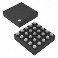


 工商网监
湘ICP备2023018690号
工商网监
湘ICP备2023018690号
