User's Guide
SNAU148A – JUNE 2013 – Revised JULY 2013
TPL5100EVM User's Guide
1
Introduction
The Texas Instruments TPL5100EVM evaluation module (EVM) allows a designer to configure the delay
timers of the TPL5100 and measure its very low current consumption. Moreover the TPL5100EVM is
ready to be connected to the Launchpads of MSP430, Stellaris and C2000, in order to test its watchdog,
timer cycling and power cycling features.
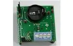
Figure 1. The LMP91010 Evaluation Board
2
Setup
This section describes how to properly connect, set up and use the TPL5100EVM.
SNAU148A – JUNE 2013 – Revised JULY 2013
Submit Documentation Feedback
TPL5100EVM User's Guide
Copyright © 2013, Texas Instruments Incorporated
1
�Setup
2.1
www.ti.com
INPUT/OUTPUT CONNECTORS AND JUMPER DESCRIPTION
I_SEL
selects the current consumption measurement method: Open, current consumption
measured with DMM connected between TP1 and VDD test points. 3-2 shorted, current
consumption = Voltage drop on R_SH divided by R_SH 1-2 R_SH bypass
5-pin header connector to bring out MOS_DRV, TCAL, DONE, VDD_µC, and GND
signals.
4 positions SPDT to set the D0, D1, D2 logic values and the source of PGOOD signal
(refer to Table 1)
IO
S1
Table 1. S1 Description
Description
Slider position
PG_SEL
D2
D1
D0
Value
Top
0
Bottom
1 or External PGOOD
Top
0
Bottom
1
Top
0
Bottom
1
Top
0
Bottom
1
In case the PGOOD is provided by an external power supply, set PG_SEL=1, Remove the REPG resistor
and connect a power supply to the EXT_PGOOD test point.
VCC
RST
J1_10
J11_20
SUPPLY
VDD
TP1
EXT_PGOOD
GND
BT
2.2
2- pin female connector to plug the TPL5100EVM into MSP430 launchpad.
2- pin female connector to plug the TPL5100EVM into MSP430 launchpad.
10-pin female connector to plug the TPL5100EVM into MSP430 launchpad.
10-pin female connector to plug the TPL5100EVM into MSP430 launchpad.
test point to connect external supply voltage in alternative to the coin cell battery.
test point to monitor VDD pin of TPL5100.
test point to monitor the external supply voltage or coin cell battery voltage.
test point to connect external voltage supply for PGOOD signal.
test point of the ground, connect here the GND of the power supplies.
coin cell 2032 battery holder.
EVALUATION BOARD CONFIGURATION
The evaluation board can work standalone or plugged in to MSP430 launchpad, the following steps are in
common for both usages.
• Set the desired delay, configuring S1 (from position 2 to 4).
• Set the POWER GOOD source, configuring S1 (position 1), if you set external source connect the
voltage source between the EXT_PGOOD and GND test points; do not turn on this voltage source.
Refer to the data sheet regarding the allowable voltage range. This can be found on the MSP430
LaunchPad Wiki (MSP430 LaunchPad (MSP-EXP430G2) Wiki).
• Configure I_SEL as explained in Section 2.1.
• Plug the evaluation board into the launchpad according to Table 2
2.2.1
EVM Plugged into MSP430 Launchpad
•
2
Load the code present in Section 5 of this User™s Guide, into the MSP430 of the launchpad. Refer to
the MSP430 launchpad documentation (MSP430 LaunchPad (MSP-EXP430G2) Wiki) for more details.
TPL5100EVM User's Guide
SNAU148A – JUNE 2013 – Revised JULY 2013
Submit Documentation Feedback
Copyright © 2013, Texas Instruments Incorporated
�Supply Current Measurement
www.ti.com
•
•
•
•
•
Remove the jumpers VCC and RST of J3 header of the launchpad
Set the desired delay, configuring S1 (from position 2 to 4).
Set the POWER GOOD source, configuring S1 (position 1), if you set external source connect the
voltage source between the EXT_PGOOD and GND test points; do not turn on this voltage source.
Refer to the data sheet regarding the allowable voltage range. This can be found on the MSP430
LaunchPad Wiki (MSP430 LaunchPad (MSP-EXP430G2) Wiki).
Configure I_SEL as explained in Section 2.1.
Plug the eval board in to the launchpad according to Table 2
Table 2. TPL5100EVM to Launchpad Connection
•
•
2.2.1.1
TPL5100EVM
MSP430 Launchpad
J1_10
J1
J11_20
J2
VCC
VCC of J3
RST
RST of J3
Insert a 2032 coin cell battery in the battery holder (BT) or alternatively connect a voltage source
between the SUPPLY and GND test points. DO NOT CONNECT THE COIN CELL BATTERY AND
THE VOLTAGE SOURCE TO SUPPLY THE EVALUATION BOARD AT SAME TIME.
Power on the voltage sources connected to the EVM.
SOFTWARE OF THE MSP430
The code in Section 5 of this User's Guide, once loaded into the MSP430 of the launchpad, performs the
following features:
• At power on, the red LED present on the Launchpad is turned ON.
• The red LED is turned off when the TPL5100 turns off the MSP430.
2.2.2
EVM Standalone
•
•
•
•
3
Connect your micro controller to IO header, in order to manage the I/O signal of the DUT.
Insert a 2032 coin cell battery in the battery holder (BT), or alternatively connect a voltage source
between the SUPPLY and GND test points. DO NOT CONNECT THE COIN CELL BATTERY AND
THE VOLTAGE SOURCE TO SUPPLY THE EVALUATION BOARD AT SAME TIME.
Power on the voltage sources connected to the EVM.
DO NOT LEAVE DONE PIN (4th pin of IO header) FLOATING. If supervisor feature is not needed,
connect DONE pin to GND.
Supply Current Measurement
The TPL5100EVM offers 2 ways to measure the current consumption of the DUT. First, disconnect the
TPL5100 from the launchpad or your micro controller, in order to not load the digital output pins of the
DUT.
3.1
DIRECT MEASUREMENT
•
•
•
•
Leave the I_SEL 3-pin header open.
DO NOT LEAVE DIGITAL INPUT PINS FLOATING, for instance:
– Short the DONE pin (4th pin of IO header) to GND
– Set PGOOD =1 (see Table 1)
Connect a Digital Multi Meter, configured as the current meter (able to measure nA), between TP1 and
VDD test points.
Read the current consumption on the DMM.
SNAU148A – JUNE 2013 – Revised JULY 2013
Submit Documentation Feedback
TPL5100EVM User's Guide
Copyright © 2013, Texas Instruments Incorporated
3
�Bill of Materials (BOM)
3.2
INDIRECT MEASUREMENT
•
•
Short pin 2 and 3 of I_SEL.
DO NOT LEAVE DIGITAL INPUT PINS FLOATING, for instance:
– Short the DONE pin (4th pin of IO header) to GND
– Set PGOOD =1 (see Table 1)
Connect a Digital Multi Meter, configured as the voltage meter, between TP1 and VDD test points.
Read the voltage drop on the R_SH on the DMM.
The current consumption is simply the voltage drop on R_SH, divided by 1Mohm.
•
•
•
4
www.ti.com
Bill of Materials (BOM)
Table 3. Bill of Material TPL5100EVM
5
DESIGNATO
R
DESCRIPTION
PART NUMBER
MANUFACTURER
QUANTITY
BT
HOLDER COINCELL 2032
RETAINRCLIP
BS-7
Memory Protection
Devices
1
C1, C2
CAP CER 0.1UF 6.3V 10%
X5R 0402
C1005X5R0J104K05
0BA
TDK
2
EXT_PGOOD
, SUPPLY,
TP1, VDD
TEST POINT PC MINI .040
5000
Keystone
4
GND
TEST POINT PC MINI .040
5001
Keystone
1
IO
CONN HEADER 5POS .100
TSW-105-07-G-S
Samtec, Inc.
1
I_SEL
CONN HEADER 3POS .100
TSW-103-07-G-S
Samtec, Inc.
1
J1_10,
J11_20
Connector, Receptacle, 100mil,
10x1, Gold plated, TH
SSW-110-01-G-S
Samtec, Inc.
2
R2, R3
RES 1.0K OHM 1/16W 5%
0402 SMD
CRCW04021K00JNE
D
Vishay-Dale
2
R4
RES 49.9K OHM 1/16W 1%
0402 SMD
CRCW040249K9FKE
D
Vishay-Dale
1
REPG
RES 0.0 OHM 1/16W JUMP
0402 SMD
CRCW04020000Z0E
D
Vishay-Dale
1
RST, VCC
CONN RECEPT 2POS .100
VERT DUAL
5-534206-1
TE Connectivity
2
R_SH
RES 1.00M OHM 1/10W 1%
0603 SMD
CRCW06031M00FKE
A
Vishay-Dale
1
S1
SWITCH SPDT GOLD
206-124
CTS Electrocomponents
1
SH-J1
SHUNT JUMPER .1
969102-0000-DA
3M
1
U1
Nano Power Programmable
Timer
TPL5100DGS
Texas Instruments
1
Example of Source Code for MSP430 present in the launchpad
#include
volatile unsigned int DONE=1;
void main(void)
{
WDTCTL = WDTPW + WDTHOLD + WDTNMI + WDTNMIES;
P1DIR
P1DIR
P1DIR
P2DIR
P2DIR
4
|=
|=
&=
&=
|=
BIT0;
BIT6;
~BIT3;
~BIT0;
BIT4;
// WDT off NMI hi/lo
// Set P1.0 to output direction RED LED
// Set P1.6 to output direction GREEN LED
// Set P1.3 S2 button to input
// Set P2.0 (WAKE) to input
// Set P2.4 (Done) to output direction
TPL5100EVM User's Guide
SNAU148A – JUNE 2013 – Revised JULY 2013
Submit Documentation Feedback
Copyright © 2013, Texas Instruments Incorporated
�Example of Source Code for MSP430 present in the launchpad
www.ti.com
P1OUT |= BIT0;
__delay_cycles(25000);
P1OUT &= ~BIT0;
// RED LED ON
// delay 25ms
// Clear P1.0 RED LED Off
//BUTTON
P1REN |=
P1IE |=
P1IES |=
P1IFG &=
//
//
//
//
S2 configuration
BIT3;
BIT3;
BIT3;
~BIT3;
Pull-up resistor enabled
P1.3 interrupt enabled
P1.3 Hi/Lo edge
P1.3 IFG cleared
// WAKE signal
P2IE |= BIT0;
P2IES &= ~BIT0;
P2IFG &= ~BIT0;
// P2.0 interrupt enabled
// P2.0 Lo/Hi edge
// P2.0 IFG cleared
// DONE signal
P2OUT |= BIT4;
__delay_cycles(100);
P2OUT &= ~BIT4;
// Done High
// delay 100u
// Done Low
IE1 |= NMIIE;
// Enable NMI
_BIS_SR(LPM4_bits + GIE);
// Enter LPM4 with Interrupt enabled
}
#pragma vector=NMI_VECTOR
__interrupt void nmi_ (void)
{
P1OUT |= BIT0;
__delay_cycles(200000);
P1OUT &= ~BIT0;
// P1.0 Red Led On
// delay 200ms
// P1.0 Red Led Off
if (DONE==1)
{
P2OUT |= BIT4;
__delay_cycles(100);
P2OUT &= ~BIT4;
}
IFG1 &= ~NMIIFG;
IE1 |= NMIIE;
// Done On
// delay 100us
// Done Off
// Re-clear NMI flag in case bounce
// Enable NMI
}
// Port 2 interrupt service routine
#pragma vector=PORT2_VECTOR
__interrupt void Port_2(void)
{
P1OUT |= BIT6;
__delay_cycles(200000);
P1OUT &= ~BIT6;
if (DONE==1)
{
P2OUT |= BIT4;
__delay_cycles(100);
P2OUT &= ~BIT4;
}
P2IES &= ~BIT0;
P2IFG &= ~BIT0;
// P1.6 Red Green On
// delay 200ms
// P1.6 Red Green Off
// Done On
// delay 100us
// Done Off
// P1.4 Lo/Hi edge
// P1.4 IFG cleared
}
// Port 1 interrupt service routine
#pragma vector=PORT1_VECTOR
__interrupt void Port_1(void)
{
SNAU148A – JUNE 2013 – Revised JULY 2013
Submit Documentation Feedback
TPL5100EVM User's Guide
Copyright © 2013, Texas Instruments Incorporated
5
�Example of Source Code for MSP430 present in the launchpad
if (DONE == 1)
{
DONE = 0;
}
else
{
DONE = 1;
}
P1IFG &= ~BIT3;
P1IES |= BIT3;
www.ti.com
// enabled/disabled and viceverasa DONE signal
// P1.3 IFG cleared
// P1.3 Hi/Lo edge
}
6
TPL5100EVM User's Guide
SNAU148A – JUNE 2013 – Revised JULY 2013
Submit Documentation Feedback
Copyright © 2013, Texas Instruments Incorporated
�www.ti.com
Appendix A Schematic
SNAU148A – JUNE 2013 – Revised JULY 2013
Submit Documentation Feedback
Schematic
Copyright © 2013, Texas Instruments Incorporated
7
�www.ti.com
Appendix B Layout
Figure 2. Layout, Top Layer, Silkscreen
8
Layout
SNAU148A – JUNE 2013 – Revised JULY 2013
Submit Documentation Feedback
Copyright © 2013, Texas Instruments Incorporated
�Appendix B
www.ti.com
Figure 3. Layout, Bottom Layer, Silkscreen
SNAU148A – JUNE 2013 – Revised JULY 2013
Submit Documentation Feedback
Layout
Copyright © 2013, Texas Instruments Incorporated
9
�EVALUATION BOARD/KIT/MODULE (EVM) ADDITIONAL TERMS
Texas Instruments (TI) provides the enclosed Evaluation Board/Kit/Module (EVM) under the following conditions:
The user assumes all responsibility and liability for proper and safe handling of the goods. Further, the user indemnifies TI from all claims
arising from the handling or use of the goods.
Should this evaluation board/kit not meet the specifications indicated in the User’s Guide, the board/kit may be returned within 30 days from
the date of delivery for a full refund. THE FOREGOING LIMITED WARRANTY IS THE EXCLUSIVE WARRANTY MADE BY SELLER TO
BUYER AND IS IN LIEU OF ALL OTHER WARRANTIES, EXPRESSED, IMPLIED, OR STATUTORY, INCLUDING ANY WARRANTY OF
MERCHANTABILITY OR FITNESS FOR ANY PARTICULAR PURPOSE. EXCEPT TO THE EXTENT OF THE INDEMNITY SET FORTH
ABOVE, NEITHER PARTY SHALL BE LIABLE TO THE OTHER FOR ANY INDIRECT, SPECIAL, INCIDENTAL, OR CONSEQUENTIAL
DAMAGES.
Please read the User's Guide and, specifically, the Warnings and Restrictions notice in the User's Guide prior to handling the product. This
notice contains important safety information about temperatures and voltages. For additional information on TI's environmental and/or safety
programs, please visit www.ti.com/esh or contact TI.
No license is granted under any patent right or other intellectual property right of TI covering or relating to any machine, process, or
combination in which such TI products or services might be or are used. TI currently deals with a variety of customers for products, and
therefore our arrangement with the user is not exclusive. TI assumes no liability for applications assistance, customer product design,
software performance, or infringement of patents or services described herein.
REGULATORY COMPLIANCE INFORMATION
As noted in the EVM User’s Guide and/or EVM itself, this EVM and/or accompanying hardware may or may not be subject to the Federal
Communications Commission (FCC) and Industry Canada (IC) rules.
For EVMs not subject to the above rules, this evaluation board/kit/module is intended for use for ENGINEERING DEVELOPMENT,
DEMONSTRATION OR EVALUATION PURPOSES ONLY and is not considered by TI to be a finished end product fit for general consumer
use. It generates, uses, and can radiate radio frequency energy and has not been tested for compliance with the limits of computing
devices pursuant to part 15 of FCC or ICES-003 rules, which are designed to provide reasonable protection against radio frequency
interference. Operation of the equipment may cause interference with radio communications, in which case the user at his own expense will
be required to take whatever measures may be required to correct this interference.
General Statement for EVMs including a radio
User Power/Frequency Use Obligations: This radio is intended for development/professional use only in legally allocated frequency and
power limits. Any use of radio frequencies and/or power availability of this EVM and its development application(s) must comply with local
laws governing radio spectrum allocation and power limits for this evaluation module. It is the user’s sole responsibility to only operate this
radio in legally acceptable frequency space and within legally mandated power limitations. Any exceptions to this are strictly prohibited and
unauthorized by Texas Instruments unless user has obtained appropriate experimental/development licenses from local regulatory
authorities, which is responsibility of user including its acceptable authorization.
For EVMs annotated as FCC – FEDERAL COMMUNICATIONS COMMISSION Part 15 Compliant
Caution
This device complies with part 15 of the FCC Rules. Operation is subject to the following two conditions: (1) This device may not cause
harmful interference, and (2) this device must accept any interference received, including interference that may cause undesired operation.
Changes or modifications not expressly approved by the party responsible for compliance could void the user's authority to operate the
equipment.
FCC Interference Statement for Class A EVM devices
This equipment has been tested and found to comply with the limits for a Class A digital device, pursuant to part 15 of the FCC Rules.
These limits are designed to provide reasonable protection against harmful interference when the equipment is operated in a commercial
environment. This equipment generates, uses, and can radiate radio frequency energy and, if not installed and used in accordance with the
instruction manual, may cause harmful interference to radio communications. Operation of this equipment in a residential area is likely to
cause harmful interference in which case the user will be required to correct the interference at his own expense.
�FCC Interference Statement for Class B EVM devices
This equipment has been tested and found to comply with the limits for a Class B digital device, pursuant to part 15 of the FCC Rules.
These limits are designed to provide reasonable protection against harmful interference in a residential installation. This equipment
generates, uses and can radiate radio frequency energy and, if not installed and used in accordance with the instructions, may cause
harmful interference to radio communications. However, there is no guarantee that interference will not occur in a particular installation. If
this equipment does cause harmful interference to radio or television reception, which can be determined by turning the equipment off and
on, the user is encouraged to try to correct the interference by one or more of the following measures:
• Reorient or relocate the receiving antenna.
• Increase the separation between the equipment and receiver.
• Connect the equipment into an outlet on a circuit different from that to which the receiver is connected.
• Consult the dealer or an experienced radio/TV technician for help.
For EVMs annotated as IC – INDUSTRY CANADA Compliant
This Class A or B digital apparatus complies with Canadian ICES-003.
Changes or modifications not expressly approved by the party responsible for compliance could void the user’s authority to operate the
equipment.
Concerning EVMs including radio transmitters
This device complies with Industry Canada licence-exempt RSS standard(s). Operation is subject to the following two conditions: (1) this
device may not cause interference, and (2) this device must accept any interference, including interference that may cause undesired
operation of the device.
Concerning EVMs including detachable antennas
Under Industry Canada regulations, this radio transmitter may only operate using an antenna of a type and maximum (or lesser) gain
approved for the transmitter by Industry Canada. To reduce potential radio interference to other users, the antenna type and its gain should
be so chosen that the equivalent isotropically radiated power (e.i.r.p.) is not more than that necessary for successful communication.
This radio transmitter has been approved by Industry Canada to operate with the antenna types listed in the user guide with the maximum
permissible gain and required antenna impedance for each antenna type indicated. Antenna types not included in this list, having a gain
greater than the maximum gain indicated for that type, are strictly prohibited for use with this device.
Cet appareil numérique de la classe A ou B est conforme à la norme NMB-003 du Canada.
Les changements ou les modifications pas expressément approuvés par la partie responsable de la conformité ont pu vider l’autorité de
l'utilisateur pour actionner l'équipement.
Concernant les EVMs avec appareils radio
Le présent appareil est conforme aux CNR d'Industrie Canada applicables aux appareils radio exempts de licence. L'exploitation est
autorisée aux deux conditions suivantes : (1) l'appareil ne doit pas produire de brouillage, et (2) l'utilisateur de l'appareil doit accepter tout
brouillage radioélectrique subi, même si le brouillage est susceptible d'en compromettre le fonctionnement.
Concernant les EVMs avec antennes détachables
Conformément à la réglementation d'Industrie Canada, le présent émetteur radio peut fonctionner avec une antenne d'un type et d'un gain
maximal (ou inférieur) approuvé pour l'émetteur par Industrie Canada. Dans le but de réduire les risques de brouillage radioélectrique à
l'intention des autres utilisateurs, il faut choisir le type d'antenne et son gain de sorte que la puissance isotrope rayonnée équivalente
(p.i.r.e.) ne dépasse pas l'intensité nécessaire à l'établissement d'une communication satisfaisante.
Le présent émetteur radio a été approuvé par Industrie Canada pour fonctionner avec les types d'antenne énumérés dans le manuel
d’usage et ayant un gain admissible maximal et l'impédance requise pour chaque type d'antenne. Les types d'antenne non inclus dans
cette liste, ou dont le gain est supérieur au gain maximal indiqué, sont strictement interdits pour l'exploitation de l'émetteur.
SPACER
SPACER
SPACER
SPACER
SPACER
SPACER
SPACER
SPACER
�【Important Notice for Users of EVMs for RF Products in Japan】
】
This development kit is NOT certified as Confirming to Technical Regulations of Radio Law of Japan
If you use this product in Japan, you are required by Radio Law of Japan to follow the instructions below with respect to this product:
1.
2.
3.
Use this product in a shielded room or any other test facility as defined in the notification #173 issued by Ministry of Internal Affairs and
Communications on March 28, 2006, based on Sub-section 1.1 of Article 6 of the Ministry’s Rule for Enforcement of Radio Law of
Japan,
Use this product only after you obtained the license of Test Radio Station as provided in Radio Law of Japan with respect to this
product, or
Use of this product only after you obtained the Technical Regulations Conformity Certification as provided in Radio Law of Japan with
respect to this product. Also, please do not transfer this product, unless you give the same notice above to the transferee. Please note
that if you could not follow the instructions above, you will be subject to penalties of Radio Law of Japan.
Texas Instruments Japan Limited
(address) 24-1, Nishi-Shinjuku 6 chome, Shinjuku-ku, Tokyo, Japan
http://www.tij.co.jp
【無線電波を送信する製品の開発キットをお使いになる際の注意事項】
本開発キットは技術基準適合証明を受けておりません。
本製品のご使用に際しては、電波法遵守のため、以下のいずれかの措置を取っていただく必要がありますのでご注意ください。
1.
2.
3.
電波法施行規則第6条第1項第1号に基づく平成18年3月28日総務省告示第173号で定められた電波暗室等の試験設備でご使用いただく。
実験局の免許を取得後ご使用いただく。
技術基準適合証明を取得後ご使用いただく。
なお、本製品は、上記の「ご使用にあたっての注意」を譲渡先、移転先に通知しない限り、譲渡、移転できないものとします。
上記を遵守頂けない場合は、電波法の罰則が適用される可能性があることをご留意ください。
日本テキサス・インスツルメンツ株式会社
東京都新宿区西新宿6丁目24番1号
西新宿三井ビル
http://www.tij.co.jp
SPACER
SPACER
SPACER
SPACER
SPACER
SPACER
SPACER
SPACER
SPACER
SPACER
SPACER
SPACER
SPACER
SPACER
SPACER
SPACER
SPACER
�EVALUATION BOARD/KIT/MODULE (EVM)
WARNINGS, RESTRICTIONS AND DISCLAIMERS
For Feasibility Evaluation Only, in Laboratory/Development Environments. Unless otherwise indicated, this EVM is not a finished
electrical equipment and not intended for consumer use. It is intended solely for use for preliminary feasibility evaluation in
laboratory/development environments by technically qualified electronics experts who are familiar with the dangers and application risks
associated with handling electrical mechanical components, systems and subsystems. It should not be used as all or part of a finished end
product.
Your Sole Responsibility and Risk. You acknowledge, represent and agree that:
1.
2.
3.
4.
You have unique knowledge concerning Federal, State and local regulatory requirements (including but not limited to Food and Drug
Administration regulations, if applicable) which relate to your products and which relate to your use (and/or that of your employees,
affiliates, contractors or designees) of the EVM for evaluation, testing and other purposes.
You have full and exclusive responsibility to assure the safety and compliance of your products with all such laws and other applicable
regulatory requirements, and also to assure the safety of any activities to be conducted by you and/or your employees, affiliates,
contractors or designees, using the EVM. Further, you are responsible to assure that any interfaces (electronic and/or mechanical)
between the EVM and any human body are designed with suitable isolation and means to safely limit accessible leakage currents to
minimize the risk of electrical shock hazard.
Since the EVM is not a completed product, it may not meet all applicable regulatory and safety compliance standards (such as UL,
CSA, VDE, CE, RoHS and WEEE) which may normally be associated with similar items. You assume full responsibility to determine
and/or assure compliance with any such standards and related certifications as may be applicable. You will employ reasonable
safeguards to ensure that your use of the EVM will not result in any property damage, injury or death, even if the EVM should fail to
perform as described or expected.
You will take care of proper disposal and recycling of the EVM’s electronic components and packing materials.
Certain Instructions. It is important to operate this EVM within TI’s recommended specifications and environmental considerations per the
user guidelines. Exceeding the specified EVM ratings (including but not limited to input and output voltage, current, power, and
environmental ranges) may cause property damage, personal injury or death. If there are questions concerning these ratings please contact
a TI field representative prior to connecting interface electronics including input power and intended loads. Any loads applied outside of the
specified output range may result in unintended and/or inaccurate operation and/or possible permanent damage to the EVM and/or
interface electronics. Please consult the EVM User's Guide prior to connecting any load to the EVM output. If there is uncertainty as to the
load specification, please contact a TI field representative. During normal operation, some circuit components may have case temperatures
greater than 60°C as long as the input and output are maintained at a normal ambient operating temperature. These components include
but are not limited to linear regulators, switching transistors, pass transistors, and current sense resistors which can be identified using the
EVM schematic located in the EVM User's Guide. When placing measurement probes near these devices during normal operation, please
be aware that these devices may be very warm to the touch. As with all electronic evaluation tools, only qualified personnel knowledgeable
in electronic measurement and diagnostics normally found in development environments should use these EVMs.
Agreement to Defend, Indemnify and Hold Harmless. You agree to defend, indemnify and hold TI, its licensors and their representatives
harmless from and against any and all claims, damages, losses, expenses, costs and liabilities (collectively, "Claims") arising out of or in
connection with any use of the EVM that is not in accordance with the terms of the agreement. This obligation shall apply whether Claims
arise under law of tort or contract or any other legal theory, and even if the EVM fails to perform as described or expected.
Safety-Critical or Life-Critical Applications. If you intend to evaluate the components for possible use in safety critical applications (such
as life support) where a failure of the TI product would reasonably be expected to cause severe personal injury or death, such as devices
which are classified as FDA Class III or similar classification, then you must specifically notify TI of such intent and enter into a separate
Assurance and Indemnity Agreement.
Mailing Address: Texas Instruments, Post Office Box 655303, Dallas, Texas 75265
Copyright © 2013, Texas Instruments Incorporated
�IMPORTANT NOTICE
Texas Instruments Incorporated and its subsidiaries (TI) reserve the right to make corrections, enhancements, improvements and other
changes to its semiconductor products and services per JESD46, latest issue, and to discontinue any product or service per JESD48, latest
issue. Buyers should obtain the latest relevant information before placing orders and should verify that such information is current and
complete. All semiconductor products (also referred to herein as “components”) are sold subject to TI’s terms and conditions of sale
supplied at the time of order acknowledgment.
TI warrants performance of its components to the specifications applicable at the time of sale, in accordance with the warranty in TI’s terms
and conditions of sale of semiconductor products. Testing and other quality control techniques are used to the extent TI deems necessary
to support this warranty. Except where mandated by applicable law, testing of all parameters of each component is not necessarily
performed.
TI assumes no liability for applications assistance or the design of Buyers’ products. Buyers are responsible for their products and
applications using TI components. To minimize the risks associated with Buyers’ products and applications, Buyers should provide
adequate design and operating safeguards.
TI does not warrant or represent that any license, either express or implied, is granted under any patent right, copyright, mask work right, or
other intellectual property right relating to any combination, machine, or process in which TI components or services are used. Information
published by TI regarding third-party products or services does not constitute a license to use such products or services or a warranty or
endorsement thereof. Use of such information may require a license from a third party under the patents or other intellectual property of the
third party, or a license from TI under the patents or other intellectual property of TI.
Reproduction of significant portions of TI information in TI data books or data sheets is permissible only if reproduction is without alteration
and is accompanied by all associated warranties, conditions, limitations, and notices. TI is not responsible or liable for such altered
documentation. Information of third parties may be subject to additional restrictions.
Resale of TI components or services with statements different from or beyond the parameters stated by TI for that component or service
voids all express and any implied warranties for the associated TI component or service and is an unfair and deceptive business practice.
TI is not responsible or liable for any such statements.
Buyer acknowledges and agrees that it is solely responsible for compliance with all legal, regulatory and safety-related requirements
concerning its products, and any use of TI components in its applications, notwithstanding any applications-related information or support
that may be provided by TI. Buyer represents and agrees that it has all the necessary expertise to create and implement safeguards which
anticipate dangerous consequences of failures, monitor failures and their consequences, lessen the likelihood of failures that might cause
harm and take appropriate remedial actions. Buyer will fully indemnify TI and its representatives against any damages arising out of the use
of any TI components in safety-critical applications.
In some cases, TI components may be promoted specifically to facilitate safety-related applications. With such components, TI’s goal is to
help enable customers to design and create their own end-product solutions that meet applicable functional safety standards and
requirements. Nonetheless, such components are subject to these terms.
No TI components are authorized for use in FDA Class III (or similar life-critical medical equipment) unless authorized officers of the parties
have executed a special agreement specifically governing such use.
Only those TI components which TI has specifically designated as military grade or “enhanced plastic” are designed and intended for use in
military/aerospace applications or environments. Buyer acknowledges and agrees that any military or aerospace use of TI components
which have not been so designated is solely at the Buyer's risk, and that Buyer is solely responsible for compliance with all legal and
regulatory requirements in connection with such use.
TI has specifically designated certain components as meeting ISO/TS16949 requirements, mainly for automotive use. In any case of use of
non-designated products, TI will not be responsible for any failure to meet ISO/TS16949.
Products
Applications
Audio
www.ti.com/audio
Automotive and Transportation
www.ti.com/automotive
Amplifiers
amplifier.ti.com
Communications and Telecom
www.ti.com/communications
Data Converters
dataconverter.ti.com
Computers and Peripherals
www.ti.com/computers
DLP® Products
www.dlp.com
Consumer Electronics
www.ti.com/consumer-apps
DSP
dsp.ti.com
Energy and Lighting
www.ti.com/energy
Clocks and Timers
www.ti.com/clocks
Industrial
www.ti.com/industrial
Interface
interface.ti.com
Medical
www.ti.com/medical
Logic
logic.ti.com
Security
www.ti.com/security
Power Mgmt
power.ti.com
Space, Avionics and Defense
www.ti.com/space-avionics-defense
Microcontrollers
microcontroller.ti.com
Video and Imaging
www.ti.com/video
RFID
www.ti-rfid.com
OMAP Applications Processors
www.ti.com/omap
TI E2E Community
e2e.ti.com
Wireless Connectivity
www.ti.com/wirelessconnectivity
Mailing Address: Texas Instruments, Post Office Box 655303, Dallas, Texas 75265
Copyright © 2013, Texas Instruments Incorporated
�


 工商网监
湘ICP备2023018690号
工商网监
湘ICP备2023018690号
