Product
Folder
Sample &
Buy
Support &
Community
Tools &
Software
Technical
Documents
TPS22967
SLVSC42A – AUGUST 2013 – REVISED APRIL 2015
TPS22967 Single-Channel, Ultra-Low Resistance Load Switch
1 Features
3 Description
•
•
•
The TPS22967 device is a small, ultra-low RON,
single-channel load switch with controlled turnon. The
device contains an N-channel MOSFET that can
operate over an input voltage range of 0.8 V to 5.5 V
and can support a maximum continuous current of
4 A. The switch is controlled by an on/off input (ON),
which can interface directly with low-voltage control
signals. In the TPS22967, a 225-Ω pulldown resistor
is added for quick output discharge when the switch
is turned off.
1
•
•
•
•
•
•
Integrated Single-Channel Load Switch
Input Voltage Range: 0.8 V to 5.5 V
Low RON Resistance
– RON = 22 mΩ at VIN = 5 V (VBIAS = 5 V)
– RON = 22 mΩ at VIN = 3.6 V (VBIAS = 5 V)
– RON = 22 mΩ at VIN = 1.8 V (VBIAS = 5 V)
4-A Maximum Continuous Switch Current
Low Quiescent Current (50 µA)
Low Control Input Threshold Enables Use of
1.2-V, 1.8-V, 2.5-V, and 3.3-V Logic
Configurable Rise Time
Quick Output Discharge (QOD)
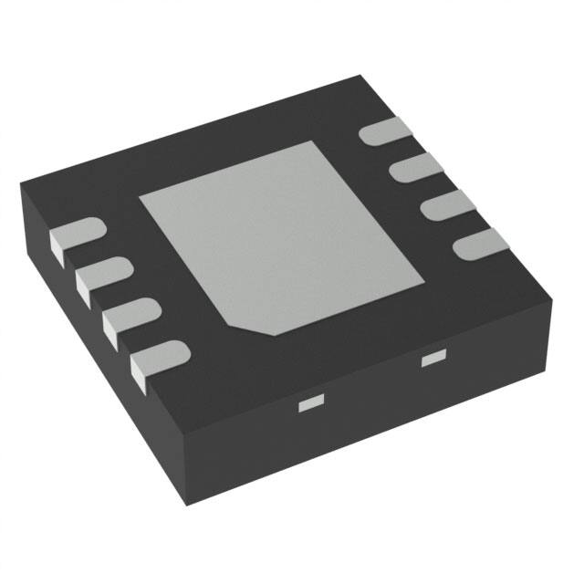
WSON 8-Pin Package With Thermal Pad
2 Applications
•
•
•
•
•
•
•
The TPS22967 is available in a small, space-saving
2-mm × 2-mm 8-pin WSON package (DSG) with
integrated thermal pad allowing for high power
dissipation. The device is characterized for operation
over the free-air temperature range of –40°C to 85°C.
Device Information(1)
PART NUMBER
TPS22967
Ultrabooks™
Notebooks and Netbooks
Tablet PCs
Consumer Electronics
Set-Top Boxes and Residental Gateways
Telecom Systems
Solid-State Drives (SSD)
PACKAGE
WSON (8)
BODY SIZE (NOM)
2.00 mm × 2.00 mm
(1) For all available packages, see the orderable addendum at
the end of the data sheet.
4 Typical Application Schematic
Power
Supply
VIN
ON
CIN
VOUT
ON
CL
RL
CT
OFF
GND
GND
VBIAS
TPS22967
1
An IMPORTANT NOTICE at the end of this data sheet addresses availability, warranty, changes, use in safety-critical applications,
intellectual property matters and other important disclaimers. PRODUCTION DATA.
�TPS22967
SLVSC42A – AUGUST 2013 – REVISED APRIL 2015
www.ti.com
Table of Contents
1
2
3
4
5
6
7
8
Features ..................................................................
Applications ...........................................................
Description .............................................................
Typical Application Schematic.............................
Revision History.....................................................
Pin Configuration and Functions .........................
Specifications.........................................................
1
1
1
1
2
3
4
7.1
7.2
7.3
7.4
7.5
7.6
7.7
7.8
4
4
4
5
5
6
7
8
Absolute Maximum Ratings ......................................
ESD Ratings..............................................................
Recommended Operating Conditions.......................
Thermal Information ..................................................
Electrical Characteristics: VBIAS = 5 V ......................
Electrical Characteristics: VBIAS = 2.5 V ...................
Switching Characteristics ..........................................
Typical Characteristics ..............................................
Detailed Description ............................................ 14
8.1
8.2
8.3
8.4
9
Overview .................................................................
Functional Block Diagram .......................................
Feature Description.................................................
Device Functional Modes........................................
14
14
14
15
Application and Implementation ........................ 16
9.1 Application Information............................................ 16
9.2 Typical Application ................................................. 17
10 Power Supply Recommendations ..................... 19
11 Layout................................................................... 19
11.1 Layout Guidelines ................................................. 19
11.2 Layout Example .................................................... 20
12 Device and Documentation Support ................. 20
12.1 Trademarks ........................................................... 20
12.2 Electrostatic Discharge Caution ............................ 20
12.3 Glossary ................................................................ 20
13 Mechanical, Packaging, and Orderable
Information ........................................................... 20
5 Revision History
Changes from Original (August 2013) to Revision A
•
2
Page
Added Pin Configuration and Functions section, ESD Ratings table, Feature Description section, Device Functional
Modes, Application and Implementation section, Power Supply Recommendations section, Layout section, Device
and Documentation Support section, and Mechanical, Packaging, and Orderable Information section .............................. 1
Submit Documentation Feedback
Copyright © 2013–2015, Texas Instruments Incorporated
Product Folder Links: TPS22967
�TPS22967
www.ti.com
SLVSC42A – AUGUST 2013 – REVISED APRIL 2015
6 Pin Configuration and Functions
DSG Package
8-Pin WSON
VIN
1
8
VOUT
VOUT
8
1
VIN
VIN
2
7
VOUT
VOUT
7
2
VIN
ON
3
6
CT
CT
6
3
ON
VBIAS
4
5
GND
GND
5
4
VBIAS
BOTTOM VIEW
TOP VIEW
Pin Functions
PIN
NAME
NO.
I/O
DESCRIPTION
CT
6
O
Switch slew rate control. Can be left floating. See Application and Implementation for more
information.
GND
5
–
Device ground.
ON
3
I
Active high switch control input. Do not leave floating.
VBIAS
4
I
Bias voltage. Power supply to the device. Recommended voltage range for this pin is 2.5 V to 5.5 V.
See Application Information section for more information.
VIN
1, 2
I
Switch input. Input capacitor recommended for minimizing VIN dip. Recommended voltage range for
this pin for optimal RON performance is 0.8 V to VBIAS.
VOUT
7, 8
O
Switch output.
–
Thermal pad (exposed center pad) to alleviate thermal stress. Tie to GND. See Layout Example for
layout guidelines.
Thermal Pad
Submit Documentation Feedback
Copyright © 2013–2015, Texas Instruments Incorporated
Product Folder Links: TPS22967
3
�TPS22967
SLVSC42A – AUGUST 2013 – REVISED APRIL 2015
www.ti.com
7 Specifications
7.1 Absolute Maximum Ratings
Over operating free-air temperature range (unless otherwise noted) (1) (2)
MIN
MAX
UNIT (2)
VIN
Input voltage
–0.3
6
V
VOUT
Output voltage
–0.3
6
V
VBIAS
Bias voltage
–0.3
6
V
VON
ON voltage
–0.3
6
V
IMAX
Maximum continuous switch current
4
A
IPLS
Maximum pulsed switch current, pulse VBIAS but it will
exhibit RON greater than what is listed in the Electrical Characteristics: VBIAS = 5 V table. See Figure 31 for an
example of a typical device. Notice the increasing RON as VIN exceeds VBIAS voltage. Never exceed the maximum
voltage rating for VIN and VBIAS.
50
VBIAS = 2.5V
VBIAS = 3.3V
45
VBIAS = 3.6V
VBIAS = 4.2V
RON (m
)
40
VBIAS = 5V
VBIAS = 5.5V
35
Temperature=25C,
IOUT=-200mA
30
25
20
0.8 1.2 1.6
2
2.4 2.8 3.2 3.6
4
4.4 4.8 5.2 5.6
VIN (V)
C017
Figure 31. RON vs VIN (VIN > VBIAS)
16
Submit Documentation Feedback
Copyright © 2013–2015, Texas Instruments Incorporated
Product Folder Links: TPS22967
�TPS22967
www.ti.com
SLVSC42A – AUGUST 2013 – REVISED APRIL 2015
Application Information (continued)
9.1.4 Safe Operating Area (SOA)
The SOA curves show the continuous current carrying capability of the device versus ambient temperature (TA)
to ensure reliable operation over 70,000 hours of device lifetime. The different curves represent the percentage
On time over device lifetime and can be used as a reference to understand the current carrying capability of
TPS22967 under different use cases. TI recommends maintaining continuous current at or below the SOA
curves shown in Figure 32.
5
Continuous Current (A)
4
3
2
100% On time
90% On time
70% On time
50% On time
30% On time
1
VBIAS=5.0V
0
-40
-15
10
35
60
85
Ambient Temperature (ºC)
C002
On time is the duration of time that the device is enabled (ON ≥ VIH) over 70,000 hour lifetime.
Figure 32. Safe Operating Area
9.2 Typical Application
Power
Supply
VIN
ON
CIN
VOUT
ON
CL
RL
CT
OFF
GND
GND
VBIAS
TPS22967
Figure 33. Typical Application Schematic
Submit Documentation Feedback
Copyright © 2013–2015, Texas Instruments Incorporated
Product Folder Links: TPS22967
17
�TPS22967
SLVSC42A – AUGUST 2013 – REVISED APRIL 2015
www.ti.com
Typical Application (continued)
9.2.1 Design Requirements
For this design example, use the parameters listed in Table 3 as the input parameters.
Table 3. Design Parameters
DESIGN PARAMETER
EXAMPLE VALUE
VIN
3.3 V
VBIAS
5V
CL
22 μF
Maximum Acceptable Inrush Current
400 mA
9.2.2 Detailed Design Procedure
9.2.2.1 Inrush Current
When the switch is enabled, the output capacitors must be charged up from 0 V to the set value (3.3 V in this
example). This charge arrives in the form of inrush current. Inrush current can be calculated using Equation 2:
Inrush Current = C × dV/dt
where
•
•
•
C = output capacitance.
dV = output voltage.
dt = rise time.
(2)
The TPS22967 offers adjustable rise time for VOUT. This feature lets the user control the inrush current during
turnon. The appropriate rise time can be calculated using the design requirements and the inrush current
equation.
400 mA = 22 μ F × 3.3 V/dt
dt = 181.5 μs
(3)
(4)
To ensure an inrush current of less than 400 mA, choose a CT value that will yield a rise time of more than 181.5
μs. See Application Curves for an example of how the CT capacitor can be used to reduce inrush current.
9.2.3 Application Curves
VBIAS = 5 V
VIN = 3.3 V
CL = 22 μF
Figure 34. Inrush Current With CT = 0 pF
18
VBIAS = 5 V
VIN = 3.3 V
CL = 22 μF
Figure 35. Inrush Current with CT = 220 pF
Submit Documentation Feedback
Copyright © 2013–2015, Texas Instruments Incorporated
Product Folder Links: TPS22967
�TPS22967
www.ti.com
SLVSC42A – AUGUST 2013 – REVISED APRIL 2015
10 Power Supply Recommendations
The device is designed to operate from a VBIAS range of 2.5 V to 5.5 V and a VIN range of 0.8 V to 5.5 V. The
power supply must be well regulated and placed as close to the device terminals as possible. It must be able to
withstand all transient and load current steps. In most situations, using an input capacitance of 1 μF is sufficient
to prevent the supply voltage from dipping when the switch is turned on. In cases where the power supply is slow
to respond to a large transient current or large load current step, additional bulk capacitance may be required on
the input.
The requirements for larger input capacitance can be mitigated by adding additional capacitance to the CT pin.
This additional capacitance causes the load switch to turn on more slowly. Not only will this reduce transient
inrush current, but it will also give the power supply more time to respond to the load current step.
11 Layout
11.1 Layout Guidelines
For best performance, all traces must be as short as possible. To be most effective, the input and output
capacitors must be placed close to the device to minimize the effects that parasitic trace inductances may have
on normal operation. Using wide traces for VIN, VOUT, and GND helps minimize the parasitic electrical effects
along with minimizing the case to ambient thermal impedance.
The maximum IC junction temperature must be restricted to 125°C under normal operating conditions. To
calculate the maximum allowable dissipation, PD(max) for a given output current and ambient temperature, use
Equation 5 as a guideline:
PD(max) =
TJ(max) - TA
θJA
where
•
•
•
•
PD(max) = maximum allowable power dissipation.
TJ(max) = maximum allowable junction temperature (125°C for the TPS22967).
TA = ambient temperature of the device.
ΘJA = junction to air thermal impedance. See Thermal Information. This parameter is highly dependent upon
board layout.
(5)
Figure 36 shows an example of a layout. Notice the thermal vias under the exposed thermal pad of the device.
This allows for thermal diffusion away from the device.
Submit Documentation Feedback
Copyright © 2013–2015, Texas Instruments Incorporated
Product Folder Links: TPS22967
19
�TPS22967
SLVSC42A – AUGUST 2013 – REVISED APRIL 2015
www.ti.com
11.2 Layout Example
Figure 36. Layout Example
12 Device and Documentation Support
12.1 Trademarks
Ultrabooks is a trademark of Intel.
All other trademarks are the property of their respective owners.
12.2 Electrostatic Discharge Caution
These devices have limited built-in ESD protection. The leads should be shorted together or the device placed in conductive foam
during storage or handling to prevent electrostatic damage to the MOS gates.
12.3 Glossary
SLYZ022 — TI Glossary.
This glossary lists and explains terms, acronyms, and definitions.
13 Mechanical, Packaging, and Orderable Information
The following pages include mechanical, packaging, and orderable information. This information is the most
current data available for the designated devices. This data is subject to change without notice and revision of
this document. For browser-based versions of this data sheet, refer to the left-hand navigation.
20
Submit Documentation Feedback
Copyright © 2013–2015, Texas Instruments Incorporated
Product Folder Links: TPS22967
�PACKAGE OPTION ADDENDUM
www.ti.com
10-Dec-2020
PACKAGING INFORMATION
Orderable Device
Status
(1)
Package Type Package Pins Package
Drawing
Qty
Eco Plan
(2)
Lead finish/
Ball material
MSL Peak Temp
Op Temp (°C)
Device Marking
(3)
(4/5)
(6)
TPS22967DSGR
ACTIVE
WSON
DSG
8
3000
RoHS & Green
NIPDAU
Level-2-260C-1 YEAR
-40 to 85
ZTU
TPS22967DSGT
ACTIVE
WSON
DSG
8
250
RoHS & Green
NIPDAU
Level-2-260C-1 YEAR
-40 to 85
ZTU
(1)
The marketing status values are defined as follows:
ACTIVE: Product device recommended for new designs.
LIFEBUY: TI has announced that the device will be discontinued, and a lifetime-buy period is in effect.
NRND: Not recommended for new designs. Device is in production to support existing customers, but TI does not recommend using this part in a new design.
PREVIEW: Device has been announced but is not in production. Samples may or may not be available.
OBSOLETE: TI has discontinued the production of the device.
(2)
RoHS: TI defines "RoHS" to mean semiconductor products that are compliant with the current EU RoHS requirements for all 10 RoHS substances, including the requirement that RoHS substance
do not exceed 0.1% by weight in homogeneous materials. Where designed to be soldered at high temperatures, "RoHS" products are suitable for use in specified lead-free processes. TI may
reference these types of products as "Pb-Free".
RoHS Exempt: TI defines "RoHS Exempt" to mean products that contain lead but are compliant with EU RoHS pursuant to a specific EU RoHS exemption.
Green: TI defines "Green" to mean the content of Chlorine (Cl) and Bromine (Br) based flame retardants meet JS709B low halogen requirements of