Product
Folder
Sample &
Buy
Support &
Community
Tools &
Software
Technical
Documents
TPS22994
SLVSCL4B – AUGUST 2014 – REVISED SEPTEMBER 2014
TPS22994 Quad Channel Load Switch with GPIO and I2C Control
1 Features
2 Applications
•
•
•
•
•
•
•
1
•
•
•
•
•
•
•
•
Input Voltage: 1.0 V to 3.6 V
Low ON-State Resistance (VBIAS = 7.2 V)
– RON = 41 mΩ at VIN = 3.3 V
– RON = 41 mΩ at VIN = 1.8 V
– RON = 41 mΩ at VIN = 1.5 V
– RON = 41 mΩ at VIN = 1.0 V
VBIAS voltage range: 2.7 V to 17.2 V
– Suitable for 1S/2S/3S/4S Li-ion Battery
Topologies
1-A Max Continuous Current Per Channel
Quiescent Current
– Single Channel < 12 µA
– All Four Channels < 22 µA
Shutdown Current (All Four Channels) < 7 µA
Four 1.2-V Compatible GPIO Control Inputs
I2C Configuration (Per Channel)
– On/Off Control
– Programmable Slew Rate Control (5 options)
– Programmable ON-delay (4 options)
– Programmable Output Discharge (4 options)
I2C SwitchALL™ Command for Multichannel/Multi-chip Control
QFN-20 package, 3 mm x 3 mm, 0.75 mm height
Ultrathin PC
Notebook PC
Tablets
Servers
All-In-One PC
3 Description
The TPS22994 is a multi-channel, low RON load
switch with user programmable features. The device
contains four N-channel MOSFETs that can operate
over an input voltage range of 1.0 V to 3.6 V. The
switch can be controlled by I2C making it ideal for
usage with processors that have limited GPIO
available. The rise time of the TPS22994 device is
internally controlled in order to avoid inrush current.
The TPS22994 has five programmable slew rate
options, four ON-delay options, and four quick output
discharge (QOD) resistance options.
The channels of the device can be controlled via
either GPIO or I2C. The default mode of operation is
GPIO control through the ONx terminals. The I2C
slave address terminals can be tied high or low to
assign seven unique device addresses.
The TPS22994 is available in a space-saving RUK
package (0.4-mm pitch) and is characterized for
operation over the free-air temperature range of
–40°C to 85°C.
Device Information(1)
PART NUMBER
TPS22994
PACKAGE
WQFN (20)
BODY SIZE (NOM)
3.00 mm x 3.00 mm
(1) For all available packages, see the orderable addendum at
the end of the datasheet.
4 Simplified Schematic
VBIAS
(2.7 V to 17.2 V)
VIN1
VOUT1
ON1
VIN2
CL
RL
CL
RL
CL
RL
CL
RL
VOUT2
ON2
PMIC or
PMU
VIN3
TPS22994
VOUT3
ON3
VOUT4
VIN4
ON4
ADD1
ADD2
SDA SCL
µC
ADD3
VDD
(1.62 to 3.6)
1
An IMPORTANT NOTICE at the end of this data sheet addresses availability, warranty, changes, use in safety-critical applications,
intellectual property matters and other important disclaimers. PRODUCTION DATA.
�TPS22994
SLVSCL4B – AUGUST 2014 – REVISED SEPTEMBER 2014
www.ti.com
Table of Contents
1
2
3
4
5
6
7
8
Features ..................................................................
Applications ...........................................................
Description .............................................................
Simplified Schematic.............................................
Revision History.....................................................
Device Comparison Table.....................................
Pin Configuration and Functions .........................
Specifications.........................................................
8.1
8.2
8.3
8.4
8.5
8.6
8.7
8.8
1
1
1
1
2
3
4
5
Recommended Operating Conditions....................... 5
Absolute Maximum Ratings ..................................... 5
Handling Ratings....................................................... 5
Thermal Information .................................................. 6
Electrical Characteristics........................................... 6
Switching Characteristics, VBIAS = 7.2 V................... 9
Switching Characteristics, VBIAS = 3.3 V .................. 9
Typical Characteristics ............................................ 11
9
Detailed Description ............................................ 18
9.1
9.2
9.3
9.4
9.5
Overview .................................................................
Functional Block Diagram .......................................
Feature Description.................................................
Device Functional Modes........................................
Register Map...........................................................
18
18
19
24
25
10 Applications and Implementation...................... 27
10.1 Application Information.......................................... 27
10.2 Typical Application ................................................ 30
11 Layout................................................................... 35
11.1 Board Layout......................................................... 35
12 Device and Documentation Support ................. 36
12.1 Trademarks ........................................................... 36
12.2 Electrostatic Discharge Caution ............................ 36
12.3 Glossary ................................................................ 36
13 Mechanical, Packaging, and Orderable
Information ........................................................... 36
5 Revision History
Changes from Revision A (September 2014) to Revision B
Page
•
Updated MAX limits in the Electrical Characteristics table. ................................................................................................... 6
•
Updated Detailed Design Procedure for Parallel Channels Application. ............................................................................. 30
Changes from Original (August 2014) to Revision A
•
2
Page
Inital release of full version datasheet. .................................................................................................................................. 1
Submit Documentation Feedback
Copyright © 2014, Texas Instruments Incorporated
Product Folder Links: TPS22994
�TPS22994
www.ti.com
SLVSCL4B – AUGUST 2014 – REVISED SEPTEMBER 2014
6 Device Comparison Table
TPS22994
RON TYPICAL AT 3.3 V (VBIAS = 7.2 V)
RISE TIME
(1)
ON DELAY
(1)
QUICK OUTPUT DISCHARGE
41 mΩ
Programmable
Programmable
(1) (2)
Programmable
MAXIMUM OUTPUT CURRENT (per channel)
1A
GPIO ENABLE
Active High
OPERATING TEMP
(1)
(2)
–40°C to 85°C
See Application Information section.
This feature discharges output of the switch to GND through an internal resistor, preventing the output from floating. See Application
information section.
Submit Documentation Feedback
Copyright © 2014, Texas Instruments Incorporated
Product Folder Links: TPS22994
3
�TPS22994
SLVSCL4B – AUGUST 2014 – REVISED SEPTEMBER 2014
www.ti.com
7 Pin Configuration and Functions
Bottom View
ON1
10
16
ADD2
ON2
9
17
SCL
ON3
8
ON4
ADD1
Exposed
Thermal Pad
GND
VIN4
VOUT4
15
VOUT3
14
VIN3
GND
13
VIN3
VIN4
12
VOUT3
VOUT4
11
Top View
15
14
13
12
11
ADD2
16
10
ON1
SCL
17
9
ON2
Exposed
Thermal Pad
VDD
18
8
ON3
19
SDA
SDA
19
7
ON4
6
20
ADD3
ADD3
20
6
ADD1
2
VIN2
1
3
VBIAS
1
VOUT2
VIN1
2
VOUT2
VOUT1
3
VIN2
4
VBIAS
5
4
5
VIN1
VDD
7
VOUT1
18
Pin Functions
Pin
NO.
NAME
Exposed Thermal
Pad
4
I/O
DESCRIPTION
-
Exposed thermal pad for thermal relief. Tie to GND.
1
VOUT2
O
Channel 2 output.
2
VIN2
I
Channel 2 input.
3
VBIAS
I
Bias voltage. Power supply to the device. Recommended voltage range for this pin is 2.7 V to 17.2 V. See
the Applications and Implementation section.
4
VIN1
I
Channel 1 input.
5
VOUT1
O
Channel 1 output.
6
ADD1
I
Device address pin. Tie high or low. Do not leave floating. See the Applications and Implementation
section.
7
ON4
I
Active high channel 4 control input. Do not leave floating.
8
ON3
I
Active high channel 3 control input. Do not leave floating.
9
ON2
I
Active high channel 2 control input. Do not leave floating.
10
ON1
I
Active high channel 1 control input. Do not leave floating.
11
VOUT4
O
Channel 4 output.
12
VIN4
I
Channel 4 input.
13
GND
-
Device ground.
14
VIN3
I
Channel 3 input.
15
VOUT3
O
Channel 3 output.
16
ADD2
I
Device address pin. Tie high or low. See the Applications and Implementation section.
17
SCL
I
Serial clock input.
18
VDD
I
I2C device supply input. Tie this pin to the I2C SCL/SDA pull-up voltage. See the Applications and
Implementation section.
19
SDA
I/O
20
ADD3
I
Serial data input/output.
Device address pin. Tie high or low. See the Applications and Implementation section.
Submit Documentation Feedback
Copyright © 2014, Texas Instruments Incorporated
Product Folder Links: TPS22994
�TPS22994
www.ti.com
SLVSCL4B – AUGUST 2014 – REVISED SEPTEMBER 2014
8 Specifications
8.1 Recommended Operating Conditions
Over operating free-air temperature range (unless otherwise noted)
VINx
Input voltage for VIN1, VIN2, VIN3,
VIN4
VBIAS
Supply voltage for VBIAS
VDD
Supply voltage for VDD
VADDx
VONx
VOUTx
CINx
(1)
MIN
MAX
For VBIAS < 4.6 V
1.0
(VBIAS – 1 V)
For VBIAS ≥ 4.6 V
1.0
3.6
UNIT
V
2.7
17.2
V
1.62
3.6
V
Input voltage for ADD1, ADD2, ADD3
0
VDD
V
Input voltage for ON1, ON2, ON3, ON4
0
5
V
Output voltage for VOUT1, VOUT2, VOUT3, VOUT4
0
VINx
V
Input capacitor on VIN1, VIN2, VIN3, VIN4
1
(1)
µF
Refer to application section.
8.2 Absolute Maximum Ratings (1)
Over operating free-air temperature range (unless otherwise noted)
VALUE
MIN
MAX
UNIT (2)
VINx
Input voltage for VIN1, VIN2, VIN3, VIN4
–0.3
4
V
VBIAS
Supply voltage for VBIAS
–0.3
20
V
VOUTx
Output voltage for VOUT1, VOUT2, VOUT3, VOUT4
–0.3
4
V
VDD, VSCL,
VSDA, VADDx
Input voltage for VDD, SCL, SDA, ADD1, ADD2, ADD3
–0.3
4
V
VONx
Input voltage for ON1, ON2, ON3, ON4
–0.3
6
V
IMAX
Maximum continuous switch current per channel
TA
Operating free-air temperature (3)
TJ
TLEAD
(1)
(2)
(3)
1
A
85
°C
Maximum junction temperature
125
°C
Maximum lead temperature (10-s soldering time)
300
°C
–40
Stresses beyond those listed under absolute maximum ratings may cause permanent damage to the device. These are stress ratings
only, and functional operation of the device at these or any other conditions beyond those indicated under recommended operating
conditions is not implied. Exposure to absolute–maximum–rated conditions for extended periods may affect device reliability.
All voltage values are with respect to network ground pin.
In applications where high power dissipation and/or poor package thermal resistance is present, the maximum ambient temperature may
have to be derated. Maximum ambient temperature [TA(max)] is dependent on the maximum operating junction temperature [TJ(max)],
the maximum power dissipation of the device in the application [PD(max)], and the junction-to-ambient thermal resistance of the
part/package in the application (θJA), as given by the following equation: TA(max) = TJ(max) – (θJA × PD(max))
8.3 Handling Ratings
Tstg
Storage temperature
ESD (1)
(1)
(2)
(3)
Electrostatic discharge protection
Human-Body Model (HBM) (2)
Charged-Device Model (CDM)
(3)
MIN
MAX
UNIT
–65
150
°C
–2000
2000
V
–-500
500
V
Electrostatic discharge (ESD) to measure device sensitivity and immunity to damage caused by assembly line electrostatic discharges in
to the device.
Level listed above is the passing level per ANSI/ESDA/JEDEC JS-001. JEDEC document JEP155 states that 500V HBM allows safe
manufacturing with a standard ESD control process.
Level listed above is the passing level per EIA-JEDEC JESD22-C101. JEDEC document JEP157 states that 250V CDM allows safe
manufacturing with a standard ESD control process.
Submit Documentation Feedback
Copyright © 2014, Texas Instruments Incorporated
Product Folder Links: TPS22994
5
�TPS22994
SLVSCL4B – AUGUST 2014 – REVISED SEPTEMBER 2014
www.ti.com
8.4 Thermal Information
TPS22994
THERMAL METRIC (1)
(2)
RUK
UNIT
20 PINS
ΘJA
Junction-to-ambient thermal resistance
46
ΘJC(top)
Junction-to-case(top) thermal resistance
50
ΘJB
Junction-to-board thermal resistance
18
ΨJT
Junction-to-top characterization parameter
0.7
ΨJB
Junction-to-board characterization parameter
18
ΘJC(bottom)
Junction-to-case(bottom) thermal resistance
4.2
(1)
(2)
°C/W
For more information about traditional and new thermal metrics, see the IC Package Thermal Metrics application report, SPRA953.
For thermal estimates of this device based on PCB copper area, see the TI PCB Thermal Calculator.
8.5 Electrical Characteristics
The specification applies over the operating ambient temperature –40°C ≤ TA ≤ 85°C (Full) (unless otherwise noted). Typical
values are for TA = 25°C. VBIAS = 7.2 V (unless otherwise noted).
PARAMETER
TEST CONDITIONS
TA
MIN
TYP
MAX
VBIAS = 2.7 V
18.3
27.6
VBIAS = 3.3 V
18.9
28.6
VBIAS = 4.5 V
19.4
29.9
VBIAS = 5.2 V
19.9
30.3
21.1
33.6
VBIAS = 10.8 V
21.2
34.8
VBIAS = 12.6 V
21.2
35.0
VBIAS = 17.2 V
21.2
35.7
VBIAS = 2.7 V
8.3
16.6
VBIAS = 3.3 V
8.8
17.6
VBIAS = 4.5 V
9.5
18.9
VBIAS = 5.2 V
9.9
19.6
11.3
22.5
VBIAS = 10.8 V
11.7
23.6
VBIAS = 12.6 V
11.7
23.8
VBIAS = 17.2 V
11.9
24.4
0.6
1.1
1.2
1.9
UNIT
POWER SUPPLIES CURRENTS AND LEAKAGES
Quiescent current for VBIAS
(all four channels)
IQ,
VBIAS
Quiescent current for VBIAS
(single channel)
IQ,
IOUT1,2,3,4 = 0 A,
VIN1,2,3,4 = lower of (VBIAS-1 V) or 3.6
V,
VON1,2,3,4 = 3.6 V,
VDD = 0 V
VDD
IDYN, VDD
IOUT1,2,3,4 = 0 A,
VIN1 = lower of (VBIAS-1 V) or 3.6 V,
VON1 = 3.6 V,
VIN2,3,4 = VON2,3,4 = 0 V,
VDD = 0 V
VBIAS = 7.2 V
VDD = 1.8 V
Quiescent current for VDD
IOUT1,2,3,4 = 0 A,
VIN1,2,3,4 = VON1,2,3,4 = 3.6 V,
fSCL = 0 Hz
Average dynamic current for
VDD during I2C
communication
IOUT1,2,3,4 = 0 A,
VIN1,2,3,4 = VON1,2,3,4 = 3.6 V,
fSCL = 1 MHz
VDD = 1.8 V
Average dynamic current for
VBIAS (all four channels)
during I2C communication
IOUT1,2,3,4 = 0 A,
VIN1,2,3,4 = lower of (VBIAS-1 V) or 3.6
V,
VON1,2,3,4 = 3.6 V,
fSCL=1 MHz
IDYN, VBIAS
Average dynamic current for
VBIAS (single channel) during
I2C communication
6
VBIAS = 7.2 V
IOUT1,2,3,4 = 0 A,
VIN1,2,3,4 = lower of (VBIAS-1 V) or 3.6
V,
VON1,2,3,4 = 3.6 V,
VIN2,3,4 = VON2,3,4 = 0 V,
fSCL= 1 MHz
VDD = 3.6 V
VDD = 3.6 V
Full
Full
Full
19.0
65.0
VBIAS = 5.2 V
66.9
VBIAS = 10.8 V
Full
68.4
68.5
VBIAS = 12.6 V
68.6
VBIAS = 17.2 V
69.1
VBIAS = 3.3 V
48.0
VBIAS = 5.2 V
58.2
VBIAS = 7.2 V
VBIAS = 10.8 V
Full
58.9
60.2
VBIAS = 12.6 V
60.2
VBIAS = 17.2 V
60.7
Submit Documentation Feedback
µA
µA
7.7
Full
VBIAS = 3.3 V
VBIAS = 7.2 V
µA
µA
µA
µA
Copyright © 2014, Texas Instruments Incorporated
Product Folder Links: TPS22994
�TPS22994
www.ti.com
SLVSCL4B – AUGUST 2014 – REVISED SEPTEMBER 2014
Electrical Characteristics (continued)
The specification applies over the operating ambient temperature –40°C ≤ TA ≤ 85°C (Full) (unless otherwise noted). Typical
values are for TA = 25°C. VBIAS = 7.2 V (unless otherwise noted).
PARAMETER
ISD,
VBIAS
Shutdown current for VBIAS
(all four channels)
ISD,
VDD
Shutdown current for VDD
ISD,
VINx
Shutdown current for VINx
TEST CONDITIONS
TA
TYP
MAX
UNIT
Full
6.5
12.8
µA
Full
1.2
1.9
µA
VINx = 3.6 V
0.005
1.0
VINx = 3.3 V
0.004
1.0
0.003
0.5
0.003
0.5
VON1,2,3,4 = 0 V, VOUT1,2,3,4 = 0 V, VDD = 3.6 V,
VBIAS = 17.2V
VON1,2,3,4 = 0 V, VOUT1,2,3,4 = 0 V,
VDD = 3.6 V
VONx = 0 V, VOUTx = 0 V, VDD = 3.6 V
VINx = 1.8 V
Full
VINx = 1.5 V
VINx = 1.0 V
MIN
µA
0.003
0.5
IONx
Leakage current for ONx
VONx = 5 V
Full
0.003
0.1
µA
IADDx
Leakage current for ADDx
VADDx = 3.6 V
Full
0.002
0.2
µA
ISCL
Leakage current for SCL
VSCL = 3.6 V
Full
0.002
0.2
µA
ISDA
Leakage current for SDA
VSDA = 3.6 V
Full
0.002
0.2
µA
25°C
40.6
50.3
RESISTANCE CHARACTERISTICS
VIN = 3.3 V
VIN = 2.5 V
VBIAS = 7.2 V, IOUT = –200 mA
VIN = 1.8 V
VIN = 1.5 V
VIN = 1.0 V
VIN = 3.3 V
VIN = 2.5 V
RON
On-state resistance
VBIAS = 5.2 V, IOUT = –200 mA
VIN = 1.8 V
VIN = 1.5 V
VIN = 1.0 V
VIN = 2.3 V
VIN = 1.8 V
VBIAS = 3.3 V, IOUT = –200 mA
VIN = 1.5 V
VIN = 1.0 V
RPD
Output pulldown resistance
Full
25°C
58.5
40.5
Full
25°C
58.5
40.5
Full
25°C
40.5
40.5
60.4
44.7
41.5
40.8
40.6
114.2
64.2
55.4
69.5
81.0
48.0
Full
57.9
70.0
VIN = 3.3 V, VON = 0 V, IOUT = 1 mA, QOD[1:0] = 00
25°C
93
VIN = 3.3 V, VON = 0 V, IOUT = 1 mA, QOD[1:0] = 01
25°C
470
VIN = 3.3 V, VON = 0 V, IOUT = 1 mA, QOD[1:0] = 10
25°C
940
VIN = 3.3 V, VON = 0 V, IOUT = 1 mA, QOD[1:0] = 11
85.9
94.4
Full
25°C
166.0
175.0
Full
25°C
50.1
60.3
Full
25°C
50.3
60.5
Full
25°C
50.3
60.9
Full
25°C
53.1
65.2
Full
25°C
64.0
71.0
Full
25°C
49.9
58.5
Full
25°C
50.1
58.5
Full
25°C
50.1
58.5
Full
25°C
50.2
Product Folder Links: TPS22994
mΩ
mΩ
mΩ
mΩ
mΩ
mΩ
mΩ
mΩ
mΩ
mΩ
mΩ
mΩ
mΩ
Ω
No
QOD
Submit Documentation Feedback
Copyright © 2014, Texas Instruments Incorporated
mΩ
7
�TPS22994
SLVSCL4B – AUGUST 2014 – REVISED SEPTEMBER 2014
www.ti.com
Electrical Characteristics (continued)
The specification applies over the operating ambient temperature –40°C ≤ TA ≤ 85°C (Full) (unless otherwise noted). Typical
values are for TA = 25°C. VBIAS = 7.2 V (unless otherwise noted).
PARAMETER
TEST CONDITIONS
TA
MIN
0.7 ×
VDD
TYP
MAX
UNIT
THRESHOLD CHARACTERISTICS
VIH,
ADDx
High-level input voltage for
ADDx
Full
VIL,
ADDx
Low-level input voltage for
ADDx
Full
VIH,
ONx
High-level input voltage for
ONx
Full
1.05
5
V
VIL,
ONx
Low-level input voltage for
ONx
Full
0
0.4
V
VHYS, ONx
Hysteresis for ONx
V
0.3×VDD
VBIAS = 2.7 V
107
VBIAS = 5.2 V
105
VBIAS = 7.2 V
VBIAS = 10.8 V
V
107
25°C
mV
108
VBIAS = 12.6 V
109
VBIAS = 17.2 V
108
2
I C CHARACTERISTICS
fSCL
(1)
Clock frequency
(1)
Setup time for SDA
(1)
Hold time for SDA
Full
tHD,
SDA
IOL,
SDA
SDA output low current
VIH,
SDA
High-level input voltage for
SDA
Full
0.7 ×
VDD
VDD
V
VIH,
SCL
High-level input voltage for
SCL
Full
0.7 ×
VDD
VDD
V
VIL,
SDA
Low-level input voltage for
SDA
Full
0
0.3×VDD
V
VIL,
SCL
Low-level input voltage for
SCL
Full
0
0.3×VDD
V
8
VOL,SDA = 0.4 V
Full
50
Full
0
MHz
SDA
(1)
fSCL = 1 MHz (fast mode plus)
1
tSU,
25°C
ns
ns
8
mA
Parameter verified by design.
Submit Documentation Feedback
Copyright © 2014, Texas Instruments Incorporated
Product Folder Links: TPS22994
�TPS22994
www.ti.com
SLVSCL4B – AUGUST 2014 – REVISED SEPTEMBER 2014
8.6 Switching Characteristics, VBIAS = 7.2 V
Values below are typical values at TA = 25°C. VBIAS = 7.2V (unless otherwise noted).
PARAMETER
tON
tOFF
tR
tF
tD
VOUTx turn-on time
VOUTx turn-off time
VOUTx rise time
VIN VOLTAGE
TEST CONDITION
VBIAS = 7.2 V,
RL= 10 Ω, CL= 0.1 µF,
QOD[1:0] = 10,
ON-delay[6:5] = 00
3.3 V
1.8 V
Slew rate[4:2] = 000
10.2
10.0
9.9
9.9
Slew rate[4:2] = 001
220
159
147
124
Slew rate[4:2] = 010
380
274
252
213
Slew rate[4:2] = 011
674
486
446
377
Slew rate[4:2] = 100
1334
967
888
749
2.5
2.5
2.5
2.5
VBIAS = 7.2 V, RL=10 Ω, CL=0.1 µF, QOD[1:0] = 10, ON-delay[6:5] =
00
VBIAS = 7.2 V, RL= 10 Ω, CL = 0.1 µF,
QOD[1:0] = 10, ON-delay[6:5] = 00
1.5 V
1.0 V
Slew rate[4:2] = 000
1.4
0.9
0.8
0.7
Slew rate[4:2] = 001
271
178
158
125
Slew rate[4:2] = 010
471
309
275
218
Slew rate[4:2] = 011
835
549
489
390
Slew rate[4:2] = 100
1674
1096
976
774
2.3
2.3
2.3
2.3
ON delay[4:2] = 00
9.6
9.6
9.6
9.6
ON delay[4:2] = 01
87
87
87
87
ON delay[4:2] = 10
295
295
295
295
ON delay[4:2] = 11
846
846
846
846
VOUTx fall time
VBIAS = 7.2 V, RL= 10 Ω, CL= 0.1 µF, QOD[1:0] = 10, ON-delay[6:5] =
00
VOUTx ON delay time
VBIAS = 7.2 V, RL= 10 Ω, CL= 0.1 µF,
QOD[1:0] = 10, Slew rate[6:5] = 000
UNIT
µs
µs
µs
µs
µs
8.7 Switching Characteristics, VBIAS = 3.3 V
Values below are typical values at TA = 25°C. VBIAS = 3.3 V (unless otherwise noted).
PARAMETER
tON
tOFF
tR
tF
VOUTx turn-on time
VOUTx turn-off time
VOUTx rise time
VOUTx fall time
VIN VOLTAGE
TEST CONDITION
VBIAS = 3.3 V,
RL=10 Ω, CL=0.1 µF,
QOD[1:0] = 10,
ON-delay[6:5] = 00
1.8V
VOUTx ON delay time
1.0V
Slew rate[4:2] = 000
8.4
8.3
8.1
Slew rate[4:2] = 001
165
152
129
Slew rate[4:2] = 010
283
260
221
Slew rate[4:2] = 011
502
460
389
Slew rate[4:2] = 100
997
915
773
VBIAS = 3.3 V, RL=10 Ω, CL=0.1 µF, QOD[1:0] = 10, ON-delay[6:5] = 00
2.5
2.6
2.8
Slew rate[4:2] = 000
2.8
2.4
1.8
Slew rate[4:2] = 001
184
163
128
Slew rate[4:2] = 010
318
283
224
Slew rate[4:2] = 011
565
501
398
Slew rate[4:2] = 100
1126
1002
791
2.2
2.2
2.1
7.3
7.3
7.3
VBIAS = 3.3 V, RL=10 Ω, CL=0.1 µF,
QOD[1:0] = 10, ON-delay[6:5] = 00
VBIAS = 3.3 V, RL=10 Ω, CL= 0.1 µF, QOD[1:0] = 10, ON-delay[6:5] = 00
ON delay[4:2] = 00
tD
1.5V
VBIAS = 3.3 V, RL=10 Ω, CL=0.1 µF,
QOD[1:0] = 10, Slew rate[6:5] = 000
ON delay[4:2] = 01
89
89
89
ON delay[4:2] = 10
296
296
296
ON delay[4:2] = 11
846
846
846
Submit Documentation Feedback
Copyright © 2014, Texas Instruments Incorporated
Product Folder Links: TPS22994
UNIT
µs
µs
µs
µs
µs
9
�TPS22994
SLVSCL4B – AUGUST 2014 – REVISED SEPTEMBER 2014
www.ti.com
V IN
V OUT
CIN = 1 µF
ON
+
-
(A)
ON
CL
RL
OFF
VBIAS
TPS22994
GND
GND
GND
Single channel shown for clarity.
A.
Rise and fall times of the control signal is 100 ns.
B.
All switching measurements are done using GPIO control only.
Figure 1. Test Circuit
VON
50%
50%
tOFF
tON
VOUT
50%
50%
tF
tR
90%
VOUT
10%
10%
90%
10%
tD
Figure 2. tON/tOFF Waveforms
10
Submit Documentation Feedback
Copyright © 2014, Texas Instruments Incorporated
Product Folder Links: TPS22994
�TPS22994
www.ti.com
SLVSCL4B – AUGUST 2014 – REVISED SEPTEMBER 2014
8.8 Typical Characteristics
1.5
1.4
1.3
1.2
1.2
1.1
1.1
1
0.9
0.8
1
0.9
0.8
0.7
0.7
0.6
0.6
0.5
0.5
0.4
1.6
1.8
2
-40°C
25°C
85°C
1.4
ISD,VDD (PA)
IQ,VDD (PA)
1.3
1.5
-40°C
25°C
85°C
2.2
VBIAS = 7.2 V
2.4
2.6 2.8
VDD (V)
3
3.2
3.4
0.4
1.6
3.6
1.8
2
2.2
2.4
D001
VINx = 3.6 V
VBIAS = 7.2 V
Figure 3. IQ,VDD vs. VDD
2.6 2.8
VDD (V)
3
3.2
3.4
3.6
D002
VINx = 3.6 V
Figure 4. ISD,VDD vs. VDD
24
14
13
22
IQ,VBIAS (PA)
IQ,VBIAS (PA)
12
20
18
11
10
9
16
14
2.7
-40°C
25°C
85°C
4.7
6.7
VINx = lower of
(VBIAS-1V) or 3.6 V
8.7
10.7
VBIAS (V)
12.7
14.7
-40°C
25°C
85°C
8
7
2.7
16.7
VDD = 3.6 V
Figure 5. IQ,VBIAS vs. VBIAS (all channels)
8.7
10.7
VBIAS (V)
12.7
14.7
16.7
D004
VDD = 3.6 V
Figure 6. IQ,VBIAS vs. VBIAS (single channel)
0.08
7.5
0.07
7
0.06
6.5
0.05
ISD,VIN (PA)
ISD,VBIAS (PA)
6.7
VINx = lower of
(VBIAS-1V) or 3.6 V
8
6
5.5
5
-40°C
25°C
85°C
0.04
0.03
0.02
-40°C
25°C
85°C
4.5
4
2.7
4.7
D003
0.01
0
4.7
VINx = lower of
(VBIAS-1V) or 3.6 V
6.7
8.7
10.7
VBIAS (V)
12.7
14.7
VDD = 3.6 V
16.7
1
1.2 1.4 1.6 1.8
D005
VBIAS = 7.2 V
2
2.2 2.4 2.6 2.8
VIN (V)
3
3.2 3.4 3.6
D006
VDD = 3.6 V
Figure 8. ISD,VIN vs. VIN
Figure 7. ISD,VBIAS vs. VBIAS
Submit Documentation Feedback
Copyright © 2014, Texas Instruments Incorporated
Product Folder Links: TPS22994
11
�TPS22994
SLVSCL4B – AUGUST 2014 – REVISED SEPTEMBER 2014
www.ti.com
Typical Characteristics (continued)
50
48
47
44
44
RON (m:)
RON (m:)
41
40
36
38
35
32
32
29
-40qC
25qC
85qC
-40°C
25°C
85°C
26
23
28
1
1.3
1.6
1.9
VBIAS = 7.2 V
2.2
2.5
VIN (V)
2.8
3.1
1
3.4 3.6
IOUT = 200 mA
Figure 9. RON vs. VIN
1.9
2.2
2.5
VIN (V)
2.8
3.1
3.4 3.6
D008
IOUT = 1 A
Figure 10. RON vs. VIN (single channel)
0.825
VBIAS = 2.7V
VBIAS = 3.3V
VBIAS = 4.5V
VBIAS = 5.2V
VBIAS = 7.2V
150
VBIAS = 10.8V
VBIAS = 12.6V
VBIAS = 14V
VBIAS = 17.2V
VIL,ONx
VIH,ONx
0.8
0.775
Threshold (V)
130
RON (m:)
1.6
VBIAS = 7.2 V
170
110
90
70
0.75
0.725
0.7
0.675
50
0.65
30
1
1.2 1.4 1.6 1.8
2
2.2 2.4 2.6 2.8
VIN (V)
3
0.625
2.7
3.2 3.4 3.6
4.7
6.7
D009
TA = 25°C
VINx = lower of
(VBIAS-1 V) or 3.6 V
Figure 11. RON vs. VIN
8.7
10.7
VBIAS (V)
12.7
14.7
16.7
D010-011
TA = 25°C
Figure 12. VIH/VIL for ONx vs. VBIAS
1200
0.15
0.14
QOD = 00
QOD = 01
QOD = 10
4.7
8.7
10.7
VBIAS (V)
12.7
1000
0.13
0.12
800
0.11
RPD (:)
VHYS,ONx (V)
1.3
D007
0.1
0.09
600
400
0.08
0.07
200
0.06
0.05
2.7
4.7
VINx = lower of
(VBIAS-1 V) or 3.6 V
6.7
8.7
10.7
VBIAS (V)
14.7
ONx
16.7
0
2.7
D012
TA = 25°C
Figure 13. VHYS,
12
12.7
6.7
14.7
16.7
D013
TA = 25°C
Figure 14. RPD vs. VBIAS
vs. VBIAS
Submit Documentation Feedback
Copyright © 2014, Texas Instruments Incorporated
Product Folder Links: TPS22994
�TPS22994
www.ti.com
SLVSCL4B – AUGUST 2014 – REVISED SEPTEMBER 2014
Typical Characteristics (continued)
1.8
3
-40°C
25°C
85°C
1.6
1.4
2.6
tR (Ps)
tR (Ps)
-40°C
25°C
85°C
2.8
1.2
2.4
1
2.2
0.8
2
0.6
1.8
1
1.3
1.6
1.9
2.2
2.5
VIN (V)
VBIAS = 7.2 V
Slew rate[4:2] =
000
2.8
3.1
3.4 3.6
1
1.1
1.2
RL = 10 Ω
VDD = 3.6 V
VBIAS = 3.3 V
Slew rate[4:2] =
000
1.4
VIN (V)
1.5
1.6
1.7
1.8
D014b
RL = 10 Ω
VDD = 3.6 V
Figure 15. tR vs. VIN
Figure 16. tR vs. VIN
200
350
-40°C
25°C
85°C
325
300
-40°C
25°C
85°C
190
180
275
250
tR (Ps)
tR (Ps)
1.3
D014a
225
200
175
170
160
150
150
140
125
130
100
1
1.2 1.4 1.6 1.8
VBIAS = 7.2 V
Slew rate[4:2] =
001
2
2.2 2.4 2.6 2.8
VIN (V)
3
1
3.2 3.4 3.6
1.1
1.2
1.3
D015a
RL = 10 Ω
VDD = 3.6 V
VBIAS = 3.3 V
Slew rate[4:2] =
001
1.4
VIN (V)
1.5
1.6
1.7
D014b
D015b
RL = 10 Ω
VDD = 3.6 V
Figure 17. tR vs. VIN
1.8
Figure 18. tR vs. VIN
340
520
-40°C
25°C
85°C
480
-40°C
25°C
85°C
320
440
300
tR (Ps)
tR (Ps)
400
360
320
280
260
280
240
240
220
200
1
1.3
VBIAS = 7.2 V
Slew rate[4:2] =
010
1.6
1.9
2.2
2.5
VIN (V)
2.8
VDD = 3.6 V
3.1
3.4 3.6
1
1.1
D016a
RL = 10 Ω
VBIAS = 3.3 V
Slew rate[4:2] =
010
Figure 19. tR vs. VIN
1.2
1.3
1.4
VIN (V)
1.5
1.6
VDD = 3.6 V
1.7
1.8
D016b
D014b
RL = 10 Ω
Figure 20. tR vs. VIN
Submit Documentation Feedback
Copyright © 2014, Texas Instruments Incorporated
Product Folder Links: TPS22994
13
�TPS22994
SLVSCL4B – AUGUST 2014 – REVISED SEPTEMBER 2014
www.ti.com
Typical Characteristics (continued)
600
960
-40°C
25°C
85°C
880
-40°C
25°C
85°C
560
800
520
tR (Ps)
tR (Ps)
720
640
560
480
440
480
400
400
360
320
1
1.3
1.6
1.9
2.2
2.5
VIN (V)
VBIAS = 7.2 V
Slew rate[4:2] =
011
2.8
3.1
1
3.4 3.6
1.1
1.2
1.3
D017a
RL = 10 Ω
VDD = 3.6 V
VBIAS = 3.3 V
Slew rate[4:2] =
011
1.4
VIN (V)
1.5
1.6
1.7
D017b
D014b
RL = 10 Ω
VDD = 3.6 V
Figure 21. tR vs. VIN
1.8
Figure 22. tR vs. VIN
1200
1920
-40°C
25°C
85°C
1760
-40°C
25°C
85°C
1120
1600
1040
tR (Ps)
tR (Ps)
1440
1280
1120
960
880
960
800
800
720
640
1
1.3
1.6
1.9
VBIAS = 7.2 V
Slew rate[4:2] =
100
2.2
2.5
VIN (V)
2.8
3.1
1
3.4 3.6
1.1
1.2
D018a
RL = 10 Ω
VDD = 3.6 V
VBIAS = 3.3 V
Slew rate[4:2] =
100
12
92
10
90
8
88
tD (PA)
tD (PA)
1.5
1.6
1.7
1.8
D014b
D018b
RL = 10 Ω
Figure 24. tR vs. VIN
94
6
4
86
84
-40°C
25°C
85°C
2
4.7
ON-delay[6:5] = 00
6.7
8.7
10.7
VBIAS (V)
12.7
VDD = 3.6 V
14.7
-40°C
25°C
85°C
82
16.7
80
2.7
4.7
D019
RL = 10 Ω
ON-delay[6:5] = 01
Figure 25. tD vs. VBIAS
14
1.4
VIN (V)
VDD = 3.6 V
Figure 23. tR vs. VIN
14
0
2.7
1.3
6.7
8.7
10.7
VBIAS (V)
12.7
VDD = 3.6 V
14.7
16.7
D020
RL = 10 Ω
Figure 26. tD vs. VBIAS
Submit Documentation Feedback
Copyright © 2014, Texas Instruments Incorporated
Product Folder Links: TPS22994
�TPS22994
www.ti.com
SLVSCL4B – AUGUST 2014 – REVISED SEPTEMBER 2014
Typical Characteristics (continued)
310
880
306
870
302
860
850
294
tD (PA)
tD (PA)
298
290
286
840
830
282
820
278
-40°C
25°C
85°C
274
270
2.7
4.7
6.7
8.7
10.7
VBIAS (V)
ON-delay[6:5] = 10
V
12.7
14.7
-40°C
25°C
85°C
810
800
2.7
16.7
4.7
RL = 10 Ω
VDD = 3.6 V
8.7
10.7
VBIAS (V)
ON-delay[6:5] = 11
12.7
14.7
16.7
D022
RL = 10 Ω
VDD = 3.6 V
Figure 28. tD vs. VBIAS
Figure 27. tD vs. VBIAS
14
10.5
-40°C
25°C
85°C
13
-40°C
25°C
85°C
10
9.5
tON (Ps)
12
tON (Ps)
6.7
D021
11
9
8.5
10
8
9
7.5
8
7
1
1.3
1.6
1.9
2.2
2.5
VIN (V)
VBIAS = 7.2 V
Slew rate[4:2] =
000
2.8
3.1
3.4 3.6
1
1.1
1.2
1.3
D023a
RL = 10 Ω
VDD = 3.6 V
VBIAS = 3.3 V
Slew rate[4:2] =
000
1.4
VIN (V)
1.5
1.6
1.7
D023b
RL = 10 Ω
VDD = 3.6 V
Figure 29. tON vs. VIN
1.8
Figure 30. tON vs. VIN
190
275
-40°C
25°C
85°C
250
-40°C
25°C
85°C
180
170
tON (Ps)
tON (Ps)
225
200
175
160
150
140
150
130
120
125
1
1.2 1.4 1.6 1.8
VBIAS = 7.2 V
Slew rate[4:2] =
001
2
2.2 2.4 2.6 2.8
VIN (V)
VDD = 3.6 V
3
3.2 3.4 3.6
1
1.1
D024a
RL = 10 Ω
VBIAS = 3.3 V
Slew rate[4:2] =
001
Figure 31. tON vs. VIN
1.2
1.3
1.4
VIN (V)
1.5
1.6
VDD = 3.6 V
1.7
1.8
D024b
RL = 10 Ω
Figure 32. tON vs. VIN
Submit Documentation Feedback
Copyright © 2014, Texas Instruments Incorporated
Product Folder Links: TPS22994
15
�TPS22994
SLVSCL4B – AUGUST 2014 – REVISED SEPTEMBER 2014
www.ti.com
Typical Characteristics (continued)
190
275
-40°C
25°C
85°C
250
-40°C
25°C
85°C
180
170
tON (Ps)
tON (Ps)
225
200
175
160
150
140
150
130
120
125
1
1.2 1.4 1.6 1.8
2
VBIAS = 7.2 V
Slew rate[4:2] =
010
2.2 2.4 2.6 2.8
VIN (V)
3
1
3.2 3.4 3.6
1.1
1.2
RL = 10 Ω
VDD = 3.6 V
VBIAS = 3.3 V
Slew rate[4:2] =
010
1.6
1.7
1.8
D024b
RL = 10 Ω
Figure 34. tON vs. VIN
-40°C
25°C
85°C
700
-40°C
25°C
85°C
540
520
500
tON (Ps)
650
tON (Ps)
1.5
560
750
600
550
480
460
500
440
450
420
400
400
380
350
1
1.2 1.4 1.6 1.8
2
VBIAS = 7.2 V
Slew rate[4:2] =
011
2.2 2.4 2.6 2.8
VIN (V)
3
1
3.2 3.4 3.6
1.1
RL = 10 Ω
VDD = 3.6 V
1320
tON (Ps)
1200
1080
960
840
720
1.2 1.4 1.6 1.8
VBIAS = 7.2 V
Slew rate[4:2] =
100
2
2.2 2.4 2.6 2.8
VIN (V)
VDD = 3.6 V
1.4
VIN (V)
1.5
1.6
1.7
1.8
D026b
RL = 10 Ω
VDD = 3.6 V
Figure 36. tON vs. VIN
-40°C
25°C
85°C
1
1.3
VBIAS = 3.3 V
Slew rate[4:2] =
011
Figure 35. tON vs. VIN
1440
1.2
D026a
1560
tON (Ps)
1.4
VIN (V)
VDD = 3.6 V
Figure 33. tON vs. VIN
800
3
3.2 3.4 3.6
1125
1100
1075
1050
1025
1000
975
950
925
900
875
850
825
800
775
750
-40°C
25°C
85°C
1
1.1
D027a
RL = 10 Ω
VBIAS = 3.3 V
Slew rate[4:2] =
100
Figure 37. tON vs. VIN
16
1.3
D024a
1.2
1.3
1.4
VIN (V)
1.5
1.6
VDD = 3.6 V
1.7
1.8
D027b
RL = 10 Ω
Figure 38. tON vs. VIN
Submit Documentation Feedback
Copyright © 2014, Texas Instruments Incorporated
Product Folder Links: TPS22994
�TPS22994
www.ti.com
SLVSCL4B – AUGUST 2014 – REVISED SEPTEMBER 2014
Typical Characteristics (continued)
4
4
-40°C
25°C
85°C
-40°C
25°C
85°C
3.5
3
3
2.5
2.5
tF (Ps)
tF (Ps)
3.5
2
2
1.5
1.5
1
1
0.5
0.5
0
0
1
1.2 1.4 1.6 1.8
VBIAS = 7.2 V
2
2.2 2.4 2.6 2.8
VIN (V)
3
3.2 3.4 3.6
1
1.1
RL = 10 Ω
VDD = 3.6 V
VBIAS = 3.3 V
Figure 39. tF vs. VIN
1.3
1.4
VIN (V)
1.5
1.6
1.7
1.8
D028b
RL = 10 Ω
VDD = 3.6 V
Figure 40. tF vs. VIN
4
4
3.5
3.5
3
3
2.5
2.5
tOFF (Ps)
tOFF (Ps)
1.2
D028a
2
1.5
2
1.5
1
1
-40°C
25°C
85°C
0.5
0
-40°C
25°C
85°C
0.5
0
1
1.3
VBIAS = 7.2 V
1.6
1.9
2.2
2.5
VIN (V)
2.8
VDD = 3.6 V
3.1
3.4 3.6
1
1.08 1.16 1.24 1.32
D029a
RL = 10 Ω
VBIAS = 3.3 V
Figure 41. tOFF vs. VIN
1.4 1.48 1.56 1.64 1.72
VIN (V)
VDD = 3.6 V
1.8
D029b
RL = 10 Ω
Figure 42. tOFF vs. VIN
Submit Documentation Feedback
Copyright © 2014, Texas Instruments Incorporated
Product Folder Links: TPS22994
17
�TPS22994
SLVSCL4B – AUGUST 2014 – REVISED SEPTEMBER 2014
www.ti.com
9 Detailed Description
9.1 Overview
The TPS22994 is a GPIO controllable and I2C programmable, quad-channel load switch. The device comes in a
20-pin QFN package and is designed to handle up to 3.6 V and 1 A per channel (per VINx/VOUTx). The VBIAS
pin of the device is designed to interface directly with battery voltages or adapter input voltages as high as 17.2
V. To increase efficiency during standby power, the device implements each channel with an N-channel
MOSFET without the use of a chargepump. This allows the quiescent current (IQ,VBIAS) to be much lower than
traditional GPIO-based load switches, thus increasing efficiency during standby.
The TPS22994 can be programmed via standard I2C commands. This allows the user to select between 5 slew
rates, 4 on-delays, and 4 quick output discharge (QOD) options. The combination of these options allows the
user to program the power sequencing for downstream modules via software. Each individual channel can also
be controlled (enabling and disabling channels only) via GPIO when I2C communication is not present. The
TPS22994 contains a special function called SwitchALLTM that allows multiple devices (either the TPS22993 or
TPS22994) to be enabled or disabled synchronously via a single I2C command, allowing the user to switch
system power states synchronously.
9.2 Functional Block Diagram
Power supply
and bandgap
VBIAS
VIN1
Driver
VOUT1
PD_EN
ON1
ON2
ON3
VIN2
GPIO ON
Buffer
Driver
ON4
VOUT2
PD_EN
ADD1
ADD2
ADD3
Address
Buffers &
Level Shifters
I2C
Digital Control
VIN3
Driver
VDD
SCL
SDA
VOUT3
I2C
SCL/SDA
Buffers &
Level Shifters
PD_EN
VIN4
Driver
VOUT4
PD_EN
* PD_EN = Pulldown Enable
18
Submit Documentation Feedback
Copyright © 2014, Texas Instruments Incorporated
Product Folder Links: TPS22994
�TPS22994
www.ti.com
SLVSCL4B – AUGUST 2014 – REVISED SEPTEMBER 2014
9.3 Feature Description
9.3.1 Operating Frequency
The TPS22994 is designed to be compatible with fast-mode plus and operate up to 1 MHz clock frequency for
bus communication. The device is also compatible with standard-mode (100 kHz) and fast-mode (400 kHz). This
device can reside on the same bus as high-speed mode (3.4MHz) devices, but the device is not designed to for
I2C commands for frequencies greater than 1 MHz. See table below for characteristics of the fast-mode plus,
fast-mode, and standard-mode bus speeds.
Table 1. I2C Interface Timing Requirements (1)
STANDARD
MODE
I2C BUS
PARAMETER
MIN
MAX
100
2
FAST MODE
PLUS (FM+)
I2C BUS
FAST MODE
I2C BUS
MIN
MAX
0
400
UNIT
MIN
MAX
0
1000
fscl
I C clock frequency
0
tsch
I2C clock high time
4
0.6
0.26
μs
tscl
I2C clock low time
4.7
1.3
0.5
μs
2
50
tsp
I C spike time
tsds
I2C serial data setup time
tsdh
I2C serial data hold time
ticr
I2C input rise time
tbuf
I2C bus free time between Stop and Start
4.7
1.3
0.5
μs
tsts
I2C Start or repeater Start condition setup time
4.7
0.6
0.26
μs
tsth
I2C Start or repeater Start condition hold time
4
0.6
0.26
μs
(1)
ns
100
50
ns
0
0
0
ns
1000
I C Stop condition setup time
4
tvd(data) Valid data time; SCL low to SDA output valid
tvd(ack)
50
250
2
tsps
50
kHz
Valid data time of ACK condition; ACK signal from SCL
low to SDA (out) low
20
300
0.6
120
ns
μs
0.26
3.45
0.3
0.9
0.45
μs
3.45
0.3
0.9
0.45
μs
over operating free-air temperature range (unless otherwise noted)
Submit Documentation Feedback
Copyright © 2014, Texas Instruments Incorporated
Product Folder Links: TPS22994
19
�TPS22994
SLVSCL4B – AUGUST 2014 – REVISED SEPTEMBER 2014
www.ti.com
9.3.2 SDA/SCL Pin Configuration
The SDA and SCL pins of the device operate use an open-drain configuration, and therefore, need pull up
resistors to communicate on the I2C bus. The graph below shows recommended values for max pull-up resistors
(RP) and bus capacitances (Cb) to ensure proper bus communications. The SDA and SCL pins should be pulled
up to VDD through an appropriately sized RP based on the graphs below.
9.3.3 Address (ADDx) Pin Configuration
The TPS22994 can be configured with an unique I2C slave addresses by using the ADDx pins. There are 3
ADDx pins that can be tied high to VDD or low to GND (independent of each other) to get up to 7 different slave
addresses. The ADDx pins should be tied to GND if the I2C functionality of the device is not to be used. External
pull-up resistors for the ADDx are optional as the ADDx inputs are high impedance. The following table shows
the ADDx pin tie-offs with their associated slave addresses (assuming an eight bit word, where the LSB is the
read/write bit and the device address bits are the 7 MSB bits) :
Hex Address
ADD3
ADD2
ADD1
E0/E1
GND
GND
GND
E2/E3
GND
GND
VDD
E4/E5
GND
VDD
GND
E6/E7
GND
VDD
VDD
E8/E9
VDD
GND
GND
EA/EB
VDD
GND
VDD
EC/ED
VDD
VDD
GND
Invalid unique device address.
This address is the SwitchALLTM address.
EE
9.3.4 On-Delay Control
Using the I2C interface, the configuration register for each channel can be set for different ON delays for power
sequencing. The typical options for delay are as follows (see Switching Characteristics, VBIAS = 7.2 V table):
00
01
10
11
=
=
=
=
11 µs delay (default register value)
105 µs delay
330 µs delay
950 µs delay
It is not recommended to change the delay value for the duration of the delay that is programmed when the
channel is enabled (except for ON-delay setting of '00' which requires a minimum of 100µs wait time before
changing the setting). This could result in erratic behavior where the output could toggle unintentionally but would
eventually recover by the end of the delay time programmed at the time of channel enable.
9.3.5 Slew Rate Control
Using the I2C interface, the configuration register for each channel can be set for different slew rates for inrush
current control and power sequencing. The typical options for slew rate are as follows (see Switching
Characteristics table for VOUTx rise times):
20
Submit Documentation Feedback
Copyright © 2014, Texas Instruments Incorporated
Product Folder Links: TPS22994
�TPS22994
www.ti.com
000
001
010
011
100
101
110
111
=
=
=
=
=
=
=
=
SLVSCL4B – AUGUST 2014 – REVISED SEPTEMBER 2014
1 µs/V
150 µs/V
250 µs/V
460 µs/V (default register value)
890 µs/V
invalid slew rate
invalid slew rate
reserved
9.3.6 Quick Output Discharge (QOD) Control
Using the I2C interface, the configuration register for each channel can be set for different output discharge
resistors. The typical options for QOD are as follows (see Electrical Characteristics table):
00
01
10
11
=
=
=
=
110 Ω
490 Ω
951 Ω (default register value)
No QOD (high impedance)
9.3.7 Mode Registers
Using the I2C interface, the mode registers can be programmed to the desired on/off status for each channel.
The contents of these registers are copied over to the control registers when a SwitchALL™ command is issued,
allowing all channels of the device to transition to their desired output states synchronously. See the I2C Protocol
section and the Application Scenario section for more information on how to use the mode registers in
conjunction with the SwitchALLTM command.
9.3.8 SwitchALL™ Command
I2C controlled channels can respond to a common slave address. This feature allows multiple load switches on
the same I2C bus to respond simultaneously. The SwitchALL™ address is EEh. During a SwitchALL™
command, the lower four bits (bits 0 through 3) of the mode register is copied to the lower four bits (bits 0
through 3) of the control register. The mode register to be invoked is referenced in the body of the SwitchALL™
command. The structure of the SwitchALL™ command is as follows (as shown in Figure 43):
. See the I2C Protocol section and the Application Scenario
section for more information on how to use the SwitchALLTM command in conjunction with the mode registers.
SCL
SwitchALLTM Address
SDA ST 1
1
1
0
Start
1
1
1
Mode Register Address
0
A D7 D6 D5 D4 D3 D2 D1 D0 A SP
W/R
Ack. from slave
Ack
from Stop
slave
Figure 43. Composition of SwitchALL™ Command
9.3.9 VDD Supply For I2C Operation
The SDA and SCL pins of the device must be pulled up to the VDD voltage of the device for proper I2C bus
communication. See Recommended Operating Conditions for VDD operating range.
Submit Documentation Feedback
Copyright © 2014, Texas Instruments Incorporated
Product Folder Links: TPS22994
21
�TPS22994
SLVSCL4B – AUGUST 2014 – REVISED SEPTEMBER 2014
www.ti.com
9.3.10 Input Capacitor (Optional)
To limit the voltage drop on the input supply caused by transient in-rush currents when the switch turns on into a
discharged load capacitor or short-circuit, a capacitor needs to be placed between VIN and GND. A 1-µF ceramic
capacitor, CIN, placed close to the pins, is usually sufficient. Higher values of CIN can be used to further reduce
the voltage drop during high-current application. When switching heavy loads, it is recommended to have an
input capacitor about 10 times higher than the output capacitor to avoid excessive voltage drop. For the fastest
slew rate setting of the device, a CIN to CL ratio of at least 100 to 1 is recommended to avoid excessive voltage
drop.
9.3.11 Output Capacitor (Optional)
Due to the integrated body diode of the NMOS switch, a CIN greater than CL is highly recommended. A CL
greater than CIN can cause VOUT to exceed VIN when the system supply is removed. This could result in current
flow through the body diode from VOUT to VIN. A CIN to CL ratio of at least 10 to 1 is recommended for minimizing
VIN dip caused by inrush currents during startup. For the fastest slew rate setting of the device, a CIN to CL ratio
of at least 100 to 1 is recommended to minimize VIN dip caused by inrush currents during startup.
9.3.12 I2C Protocol
The following section will cover the standard I2C protocol used in the TPS22994. In the I2C protocol, the following
basic blocks are present in every command (except for the SwitchALLTM command):
• Start/stop bit – marks the beginning and end of each command.
• Slave address – the unique address of the slave device.
• Sub address – this includes the register address and the auto-increment bit.
• Data byte – data being written to the register. Eight bits must always be transferred even if a single bit is
being written or read.
• Auto-increment bit – setting this bit to ‘1’ turns on the auto-increment functionality; setting this bit to ‘0’ turns
off the auto-increment functionality.
• Write/read bit – this bit signifies if the command being sent will result in reading from a register or writing to a
register. Setting this bit to ‘0’ signifies a write, and setting this bit to ‘1’ signifies a read.
• Acknowledge bit – this bit signifies if the master or slave has received the preceding data byte.
9.3.12.1
Start and Stop Bit
2
In the I C protocol, all commands contain a START bit and a STOP bit. A START bit, defined by high to low
transition on the SDA line while SCL is high, marks the beginning of a command. A STOP bit, defined by low to
high transition on the SDA line while SCL is high, marks the end of a command. The START and STOP bits are
generated by the master device on the I2C bus. The START bit indicates to other devices that the bus is busy,
and some time after the STOP bit the bus is assumed to be free.
9.3.12.2
Auto-increment Bit
The auto-increment feature in the I2C protocol allows users to read from and write to consecutive registers in
fewer clock cycles. Since the register addresses are consecutive, this eliminates the need to resend the register
address. The I2C core of the device automatically increments the register address pointer by one when the autoincrement bit is set to ‘1’. When this bit is set to ‘0’, the auto-increment functionality is disabled.
9.3.12.3
Write Command
During the write command, the write/read bit is set to ‘0’, signifying that the register in question will be written to.
Figure 44 the composition of the write protocol to a single register:
SCL
Slave Address
SDA
ST A6 A5 A4 A3 A2 A1 A0 0
Start
Sub Address
A
0
0
0
0
0
0
Data Byte
0
W/R
Ack. from slave
Register Address N
Auto-Inc.
0
Data Byte
A D7 D6 D5 D4 D3 D2 D1 D0 A D7 D6 D5 D4 D3 D2 D1 D0 A SP
Ack
from
slave
Data to Register N
Ack
from
slave
Data to Register N
Ack Stop
from
slave
Figure 44. Data Write to a Single Register
22
Submit Documentation Feedback
Copyright © 2014, Texas Instruments Incorporated
Product Folder Links: TPS22994
�TPS22994
www.ti.com
SLVSCL4B – AUGUST 2014 – REVISED SEPTEMBER 2014
Number of clock cycles for single register write: 29
If multiple consecutive registers must be written to, a short-hand version of the write command can be used.
Using the auto-increment functionality of I2C, the device will increment the register address after each byte.
Figure 45 shows the composition of the write protocol to multiple consecutive registers:
SCL
Slave Address
SDA
Sub Address
ST A6 A5 A4 A3 A2 A1 A0 0
Start
A
1
0
0
0
0
Data Byte
0
0
0
W/R
Ack. from slave
Register Address N
Auto-Inc.
Data Byte
A D7 D6 D5 D4 D3 D2 D1 D0 A D7 D6 D5 D4 D3 D2 D1 D0 A
Ack
from
slave
Data to Register N
Ack
from
slave
Data to Register N+1
Ack
from
slave
Figure 45. Data Write to Consecutive Registers
Number of clock cycles for consecutive register write: 20 + (Number of registers) x 9
The write command is always ended with a STOP bit after the desired registers have been written to. If multiple
non-consecutive registers must be written to, then the format in Figure 44 must be followed.
9.3.12.4
Read Command
During the read command, the write/read bit is set to ‘1’, signifying that the register in question will be read from.
However, a read protocol includes a “dummy” write sequence to ensure that the memory pointer in the device is
pointing to the correct register that will be read. Failure to precede the read command with a write command may
result in a read from a random register. Figure 46 shows the composition of the read protocol to a single register:
SCL
Slave Address
SDA
ST A6 A5 A4 A3 A2 A1 A0 0
Start
Sub Address
A
0
0
0
W/R
Ack. from slave
Auto-Inc.
0
0
0
Slave Address
0
0
A RS A6 A5 A4 A3 A2 A1 A0 1
Data Byte
A D7 D6 D5 D4 D3 D2 D1 D0 NA SP
Ack Re-Start
W/R
Register Address from
Ack. from slave
slave
Continued
Data from Register N
Stop
No Ack. from master (message ends)
Figure 46. Data Read to a Single Register
Number of clock cycles for single register read: 39
If multiple registers must be read from, a short-hand version of the read command can be used. Using the autoincrement functionality of I2C, the device will increment the register address after each byte. Figure 47 shows the
composition of the read protocol to multiple consecutive registers:
SCL
Slave Address
SDA
ST A6 A5 A4 A3 A2 A1 A0 0
Start
Sub Address
A
1
0
W/R
Ack. from slave
Auto-Inc.
0
0
0
0
Slave Address
0
0
Data Byte
A RS A6 A5 A4 A3 A2 A1 A0 1
A D7 D6 D5 D4 D3 D2 D1 D0
Ack Re-Start
W/R
Register Address from
Ack. from slave
slave
Continued
Data Byte
Data from Register N
Data Byte
A D7 D6 D5 D4 D3 D2 D1 D0 A D7 D6 D5 D4 D3 D2 D1 D0 NA SP
Ack. from master
Data from Register N+1
Ack. from master
Data from Register N+2
Stop
No Ack. from master (Message ends)
Figure 47. Data Read to Consecutive Registers
Number of clock cycles for consecutive register write: 30 + (Number of registers) x 9
Submit Documentation Feedback
Copyright © 2014, Texas Instruments Incorporated
Product Folder Links: TPS22994
23
�TPS22994
SLVSCL4B – AUGUST 2014 – REVISED SEPTEMBER 2014
www.ti.com
The read command is always ended with a STOP bit after the desired registers have been read from. If multiple
non-consecutive registers must be read from, then the format in Figure 46 must be followed.
9.3.12.5
SwitchALLTM Command
The SwitchALLTM command allows multiple devices in the same I2C bus to respond synchronously to the same
command from the master. Every TPS22994 device has a shared address which allows for multiple devices to
respond or execute a pre-determined action with a single command. Figure 48 shows the composition of the
SwitchALLTM command:
SCL
SwitchALLTM Address
SDA ST 1
1
1
0
Start
1
1
1
Mode Register Address
0
A D7 D6 D5 D4 D3 D2 D1 D0 A SP
W/R
Ack. from slave
Ack
from Stop
slave
Figure 48. SwitchALLTM Command Structure
Number of clock cycles for a SwitchALLTM command: 20
9.4 Device Functional Modes
9.4.1 I2C Control
When power is applied to VBIAS, the device comes up in its default mode of GPIO operation where the channel
outputs can be controlled solely via the ON pins. At any time, if SDA and SCL are present and valid, the device
can be configured to be controlled via I2C (if in GPIO control) or GPIO (if in I2C control).
The control register (address 05h) can be configured for GPIO or I2C enable on a per channel basis.
9.4.2 GPIO Control
There are four ON pins to enable/disable the four channels. Each ON pin controls the state of the switch by
default upon power up. Asserting ON high enables the switch. ON is active high and has a low threshold, making
it capable of interfacing with low-voltage signals. The ON pin is compatible with standard GPIO logic threshold. It
can be used with any microcontroller with 1.2 V or higher voltage GPIO.
24
Submit Documentation Feedback
Copyright © 2014, Texas Instruments Incorporated
Product Folder Links: TPS22994
�TPS22994
www.ti.com
SLVSCL4B – AUGUST 2014 – REVISED SEPTEMBER 2014
9.5 Register Map
Configuration registers (default register values shown below)
Channel 1 configuration register (Address: 01h)
BIT
B7
DESCRIPTION
X
DEFAULT
X
B6
B5
B4
ON-DELAY
0
B3
B2
SLEW RATE
0
0
1
1
B5
B4
B3
B2
B1
B0
QUICK OUTPUT
DISCHARGE
1
0
Channel 2 configuration register (Address: 02h)
BIT
B7
DESCRIPTION
X
DEFAULT
X
B6
ON-DELAY
0
SLEW RATE
0
0
1
1
B5
B4
B3
B2
B1
B0
QUICK OUTPUT
DISCHARGE
1
0
Channel 3 configuration register (Address: 03h)
BIT
B7
DESCRIPTION
X
DEFAULT
X
B6
ON-DELAY
0
SLEW RATE
0
0
1
1
B5
B4
B3
B2
B1
B0
QUICK OUTPUT
DISCHARGE
1
0
Channel 4 configuration register (Address: 04h)
BIT
B7
DESCRIPTION
X
DEFAULT
X
B6
ON-DELAY
0
SLEW RATE
0
0
B1
B0
QUICK OUTPUT
DISCHARGE
1
0
1
1
B3
ENABLE CH
4
0
B2
ENABLE CH
3
0
B1
ENABLE CH
2
0
B0
ENABLE CH
1
0
B3
ENABLE CH
4
0
B2
ENABLE CH
3
0
B1
ENABLE CH
2
0
B0
ENABLE CH
1
0
B3
ENABLE CH
4
0
B2
ENABLE CH
3
0
B1
ENABLE CH
2
0
B0
ENABLE CH
1
0
B3
ENABLE CH
4
0
B2
ENABLE CH
3
0
B1
ENABLE CH
2
0
B0
ENABLE CH
1
0
Control register (default register values shown below)
Control register (Address: 05h)
BIT
DESCRIPTION
DEFAULT
B7
GPIO/I2C ch
4
0
B6
GPIO/I2C ch
3
0
B5
GPIO/I2C ch
2
0
B4
GPIO/I2C ch
1
0
Mode registers (default register values shown below)
Mode1 (Address: 06h)
BIT
B7
B6
B5
B4
DESCRIPTION
X
X
X
X
DEFAULT
X
X
X
X
BIT
B7
B6
B5
B4
DESCRIPTION
X
X
X
X
DEFAULT
X
X
X
X
BIT
B7
B6
B5
B4
DESCRIPTION
X
X
X
X
DEFAULT
X
X
X
X
Mode2 (Address: 07h)
Mode3 (Address: 08h)
Submit Documentation Feedback
Copyright © 2014, Texas Instruments Incorporated
Product Folder Links: TPS22994
25
�TPS22994
SLVSCL4B – AUGUST 2014 – REVISED SEPTEMBER 2014
www.ti.com
Mode4 (Address: 09h)
BIT
B7
B6
B5
B4
DESCRIPTION
X
X
X
X
DEFAULT
X
X
X
X
BIT
B7
B6
B5
B4
DESCRIPTION
X
X
X
X
DEFAULT
X
X
X
X
BIT
B7
B6
B5
B4
DESCRIPTION
X
X
X
X
DEFAULT
X
X
X
X
BIT
B7
B6
B5
B4
DESCRIPTION
X
X
X
X
DEFAULT
X
X
X
X
BIT
B7
B6
B5
B4
DESCRIPTION
X
X
X
X
DEFAULT
X
X
X
X
BIT
B7
B6
B5
B4
DESCRIPTION
X
X
X
X
DEFAULT
X
X
X
X
BIT
B7
B6
B5
B4
DESCRIPTION
X
X
X
X
DEFAULT
X
X
X
X
BIT
B7
B6
B5
B4
DESCRIPTION
X
X
X
X
DEFAULT
X
X
X
X
BIT
B7
B6
B5
B4
DESCRIPTION
X
X
X
X
DEFAULT
X
X
X
X
B3
ENABLE CH
4
0
B2
ENABLE CH
3
0
B1
ENABLE CH
2
0
B0
ENABLE CH
1
0
B3
ENABLE CH
4
0
B2
ENABLE CH
3
0
B1
ENABLE CH
2
0
B0
ENABLE CH
1
0
B3
ENABLE CH
4
0
B2
ENABLE CH
3
0
B1
ENABLE CH
2
0
B0
ENABLE CH
1
0
B3
ENABLE CH
4
0
B2
ENABLE CH
3
0
B1
ENABLE CH
2
0
B0
ENABLE CH
1
0
B3
ENABLE CH
4
0
B2
ENABLE CH
3
0
B1
ENABLE CH
2
0
B0
ENABLE CH
1
0
B3
ENABLE CH
4
0
B2
ENABLE CH
3
0
B1
ENABLE CH
2
0
B0
ENABLE CH
1
0
B3
ENABLE CH
4
0
B2
ENABLE CH
3
0
B1
ENABLE CH
2
0
B0
ENABLE CH
1
0
B3
ENABLE CH
4
0
B2
ENABLE CH
3
0
B1
ENABLE CH
2
0
B0
ENABLE CH
1
0
B3
ENABLE CH
4
0
B2
ENABLE CH
3
0
B1
ENABLE CH
2
0
B0
ENABLE CH
1
0
Mode5 (Address: 0Ah)
Mode6 (Address: 0Bh)
Mode7 (Address: 0Ch)
Mode8 (Address: 0Dh)
Mode9 (Address: 0Eh)
Mode10 (Address: 0Fh)
Mode11 (Address: 10h)
Mode12 (Address: 11h)
26
Submit Documentation Feedback
Copyright © 2014, Texas Instruments Incorporated
Product Folder Links: TPS22994
�TPS22994
www.ti.com
SLVSCL4B – AUGUST 2014 – REVISED SEPTEMBER 2014
10 Applications and Implementation
NOTE
Information in the following applications sections is not part of the TI component
specification, and TI does not warrant its accuracy or completeness. TI’s customers are
responsible for determining suitability of components for their purposes. Customers should
validate and test their design implementation to confirm system functionality.
10.1 Application Information
This section will cover applications of I2C in the TPS22994. Registers discussed here are specific to the
TPS22994.
10.1.1 Input Capacitor (Optional)
To limit the voltage drop on the input supply caused by transient in-rush currents when the switch turns on into a
discharged load capacitor or short-circuit, a capacitor needs to be placed between VIN and GND. A 1-µF ceramic
capacitor, CIN, placed close to the pins, is usually sufficient. Higher values of CIN can be used to further reduce
the voltage drop during high-current application. When switching heavy loads, it is recommended to have an
input capacitor about 10 times higher than the output capacitor to avoid excessive voltage drop. For the fastest
slew rate setting of the device, a CIN to CL ratio of at least 100 to 1 is recommended to avoid excessive voltage
drop.
10.1.2 Output Capacitor (Optional)
Due to the integrated body diode of the NMOS switch, a CIN greater than CL is highly recommended. A CL
greater than CIN can cause VOUT to exceed VIN when the system supply is removed. This could result in current
flow through the body diode from VOUT to VIN. A CIN to CL ratio of at least 10 to 1 is recommended for minimizing
VIN dip caused by inrush currents during startup. For the fastest slew rate setting of the device, a CIN to CL ratio
of at least 100 to 1 is recommended to minimize VIN dip caused by inrush currents during startup.
10.1.3 Switch from GPIO Control to I2C Control (and vice versa)
The TPS22994 can be switched from GPIO control to I2C (and vice versa) mode by writing to the control register
of the device. Each device has a single control register and is located at register address 05h. The register’s
composition is as follows:
Control register (Address: 05h)
BIT
DESCRIPTION
DEFAULT
B7
B6
B5
B4
B3
GPIO/I2C CH GPIO/I2C CH GPIO/I2C CH GPIO/I2C CH ENABLE CH
4
3
2
1
4
0
0
0
0
0
B2
ENABLE CH
3
0
B1
ENABLE CH
2
0
B0
ENABLE CH
1
0
Figure 49. Control Register Composition
The higher four bits of the control register dictates if the device is in GPIO control (bit set to ‘0’) or I2C control (bit
set to ‘1’). The transition from GPIO control to I2C control can be made with a single write command to the
control register. See Figure 44 for the composition of a single write command. It is recommended that the
channel of interest is transitioned from GPIO control to I2C control with the first write command and followed by a
second write command to enable the channel via I2C control. This will ensure a smooth transition from GPIO
control to I2C control.
10.1.4 Configuration of Configuration Registers
The TPS22994 contains four configuration registers (one for each channel) and are located at register addresses
01h through 04h. The register’s composition is as follows (single channel shown for clarity):
Submit Documentation Feedback
Copyright © 2014, Texas Instruments Incorporated
Product Folder Links: TPS22994
27
�TPS22994
SLVSCL4B – AUGUST 2014 – REVISED SEPTEMBER 2014
www.ti.com
Channel 1 configuration register (Address: 01h)
BIT
DESCRIPTION
B7
X
B6
DEFAULT
X
0
B5
B4
B3
SLEW RATE
B2
0
0
1
0
ON-DELAY
B1
B0
QUICK OUTPUT
DISCHARGE
1
0
Figure 50. Configuration Register Composition
10.1.4.1 Single Register Configuration
A single configuration register can be written to using the write command sequence shown in Figure 44.
Multiple register writes to non-consecutive registers is treated as multiple single register writes and follows the
same write command as that of a single register write as shown in Figure 44.
10.1.4.2 Multi-register Configuration (Consecutive Registers)
Multiple consecutive configuration registers can be written to using the write command sequence shown in
Figure 45.
10.1.5 Configuration of Mode Registers
The TPS22994 contains twelve mode registers located at register addresses 06h through 11h. These mode
registers allow the user to turn-on or turn-off multiple channels in a single TPS22994 or multiple channels
spanning multiple TPS22994 devices with a single SwitchALLTM command.
For example, an application may have multiple power states (e.g. sleep, active, idle, etc.) as shown in Figure 51.
SwitchALLTM command with Mode2
register
TM
SwitchALL command with Mode1
register
Sleep
Active
S
co witch
Mo mma ALL TM
de nd
2r
eg with
is t
er
TM
S
co witch
Mo mma ALL TM
de nd
3r
eg with
ist
er
L
AL ith
itch d w er
Sw man gist
re
m
co de1
Mo
TM
L
AL ith
itch d w er
Sw man gist
re
m
co de3
Mo
Idle
Figure 51. Application Example of Power States
In each of the different power states, different combinations of channels may be on or off. Each power state may
be associated with a single mode register (Mode1, Mode2, etc.) across multiple TPS22994 as shown in Table 2.
For example, with 7 quad-channel devices, up to 28 rails can be enabled/disabled with a single SwitchALLTM
command.
Table 2. Application Example of State of Each Channel in Multiple TPS22994 in Different Power States
Load Switch #1
Load Switch #2
Load Switch #N
Mode
Register
Power
State
Ch. 1
Ch. 2
Ch. 3
Ch. 4
Ch. 1
Ch. 2
Ch. 3
Ch. 4
Ch. 1
Ch. 2
Ch. 3
Ch. 4
Mode1
Sleep
Off
Off
Off
Off
Off
Off
Off
Off
Off
Off
Off
Off
Mode2
Active
On
On
On
On
On
Off
On
Off
On
Off
On
Off
Mode3
Idle
On
Off
On
Off
On
On
On
On
On
On
On
On
28
Submit Documentation Feedback
Copyright © 2014, Texas Instruments Incorporated
Product Folder Links: TPS22994
�TPS22994
www.ti.com
SLVSCL4B – AUGUST 2014 – REVISED SEPTEMBER 2014
The contents of the lower four bits of the mode register is copied into the lower four bits of the control register
during an SwitchALLTM command. The address of the mode register to be copied is specified in the SwitchALLTM
command (see Figure 48 for the structure of the SwitchALLTM command). By executing a SwitchALLTM
command, the application will apply the different on/off combinations for the various power states with a single
command rather than having to turn on/off each channel individually by re-configuring the control register. This
reduces the latency and allows the application to control multiple channels synchronously. The example above
shows the application using three mode registers, but the TPS22994 contains twelve mode registers, allowing for
up to twelve power states.
The mode register’s composition is as follows (single mode register shown for clarity):
Mode1 (Address: 06h)
BIT
DESCRIPTION
B7
X
B6
X
B5
X
B4
X
DEFAULT
X
X
X
X
B3
ENABLE
CH 4
0
B2
ENABLE
CH 3
0
B1
ENABLE
CH 2
0
B0
ENABLE
CH 1
0
Figure 52. Mode Register Composition
The lower four bits of the mode registers are copied into the lower four bits of the control register during an allcall command.
10.1.6 Turn-on/Turn-off of Channels
By default upon power up VBIAS, all the channels of the TPS22994 are controlled via the ONx pins. Using the
I2C interface, each channel be controlled via I2C control as well. The channels of the TPS22994 can also be
switched on or off by writing to the control register of the device. Each device has a single control register and is
located at register address 05h. The register’s composition is as follows:
Control Register (Address: 05h)
BIT
DESCRIPTION
DEFAULT
B7
B6
B5
B4
GPIO/I2C CH GPIO/I2C CH GPIO/I2C CH GPIO/I2C CH
4
3
2
1
0
0
0
0
B3
ENABLE CH
4
0
B2
ENABLE CH
3
0
B1
ENABLE CH
2
0
B0
ENABLE CH
1
0
Figure 53. Control Register Composition
The lower four bits of the control register dictate if the channels of the device are off (bit set to ‘0’) or on (bit set
to ‘1’) during I2C control. The transition from off to on can be made with a single write command to the control
register. See Figure 44 for the composition of a single write command.
Submit Documentation Feedback
Copyright © 2014, Texas Instruments Incorporated
Product Folder Links: TPS22994
29
�TPS22994
SLVSCL4B – AUGUST 2014 – REVISED SEPTEMBER 2014
www.ti.com
10.2 Typical Application
10.2.1 Tying Multiple Channels in Parallel
Two or more channels of the device can be tied in parallel for applications that require lower RON and/or more
continous current. Tying two channels in parallel will result in half of the RON and two times the IMAX capability.
Tying three channels in parallel will result in one-third of the RON and three times the IMAX capability. Tying four
channels in parallel will result in one-fourth of the RON and four times the IMAX capability. For the channels that
are tied in parallel, it is recommended that the ONx pins be tied together for synchronous control of the channels
when in GPIO control. In I2C control, all four channels can be enabaled or disabled synchronously by writing to
the control register of the device. Figure 54 shows an application example of tying all four channels in parallel.
VBIAS
(2.7 V to 17.2 V)
VIN1
PMIC or
PMU
VOUT1
ON1
CL
VIN2
RL
VOUT2
ON2
TPS22994
VIN3
VOUT3
ON3
VOUT4
VIN4
ON4
ADD1
GPIO >>
ADD2
SDA SCL
µC
ADD3
VDD
(1.62 to 3.6)
Figure 54. Parallel Channels
10.2.1.1 Design Requirements
Refer to Design Requirements .
10.2.1.2 Detailed Design Procedure
Refer to Detailed Design Procedure.
The only difference between single channel and multiple channels in parallel is the resulting RON and voltage
drop from VINx to VOUTx. Thus, the design procedure is identical to Detailed Design Procedure. The VINx to
VOUTx voltage drop in the device is determined by the RON of the device and the load current. The RON of the
device depends upon the VIN conditions of the device. Refer to the RON specification of the device in the
Electrical Characteristics table of this datasheet. Once the RON of the device is determined based upon the VINx
conditions, use the following equation to calculate the VINx to VOUTx voltage drop:
∆V = ILOAD × (RON/K)
(1)
Where:
ΔV = voltage drop from VINx to VOUTx
ILOAD = load current
RON = On-resistance of the device for a specific VIN
K = number of channels in parallel (2, 3, or 4)
An appropriate ILOAD must be chosen such that the IMAX specification per channel of the device is not violated.
10.2.1.3 Application Curves
Refer to Application Curves.
30
Submit Documentation Feedback
Copyright © 2014, Texas Instruments Incorporated
Product Folder Links: TPS22994
�TPS22994
www.ti.com
SLVSCL4B – AUGUST 2014 – REVISED SEPTEMBER 2014
Typical Application (continued)
10.2.2 Cold Boot Programming of All Registers
Since the TPS22994 has a digital core with volatile memory, upon power cycle of the VBIAS pin, the registers
will revert back to their default values (see register map for default values). Therefore, the application must
reprogram the configuration registers, control register, and mode registers if non-default values are desired. The
TPS22994 contains 17 programmable registers (4 configuration registers, 1 control register, 12 mode registers)
in total.
During cold boot when the microcontroller and the I2C bus is not yet up and running, the channels of the
TPS22994 can still be enabled via GPIO control. One method to achieve this is to tie the ONx pin to the
respective VINx pin for the channels that need to turn on by default during cold boot. With this method, when
VINx is applied to the TPS22994, the channel will be enabled as well. Once the I2C bus is active, the channel
can be switched over to I2C control to be disabled. See Figure 55 for an example of how the ONx pins can be
tied to VINx for default enable during cold boot.
VBIAS
(2.7 V to 17.2 V)
VIN1
VOUT1
ON1
VIN2
CL
RL
CL
RL
CL
RL
CL
RL
VOUT2
ON2
PMIC or
PMU
VIN3
TPS22994
VOUT3
ON3
VOUT4
VIN4
ON4
ADD1
ADD2
SDA SCL
µC
ADD3
VDD
(1.62 to 3.6)
Figure 55. Cold Boot Programming
10.2.2.1 Design Requirements
Refer to Design Requirements.
10.2.2.2 Detailed Design Procedure
Refer to Design Requirements.
10.2.2.3 Application Curves
Refer to Application Curves.
Submit Documentation Feedback
Copyright © 2014, Texas Instruments Incorporated
Product Folder Links: TPS22994
31
�TPS22994
SLVSCL4B – AUGUST 2014 – REVISED SEPTEMBER 2014
www.ti.com
Typical Application (continued)
10.2.3 Power Sequencing Without I2C
It is also possible to power sequence the channels of the device during a cold boot when there is no I2C bus
present for control. One method to accomplish this it to tie the VOUT of one channel to the ON pin of the next
channel in the sequence. For example, if the desired power up sequence is VOUT3, VOUT1, VOUT2, and
VOUT4 (in that order), then the device can be configured for GPIO control as shown in Figure 56. The device will
power up with default slew rate, ON-delay, and QOD values as specified in the register map.
VBIAS
(2.7 V to 17.2 V)
VIN1
VOUT1
ON1
VIN2
CL
RL
CL
RL
CL
RL
CL
RL
VOUT2
ON2
PMIC or
PMU
TPS22994
VIN3
VOUT3
ON3
VOUT4
VIN4
ON4
ADD1
ADD2
SDA SCL
µC
ADD3
VDD
(1.62 to 3.6)
Figure 56. Power Sequencing Without I2C Schematic
10.2.3.1 Design Requirements
10.2.3.1.1 Reading From the Registers
Reading any register from the TPS22994 follows the same standard I2C read protocol as outlined in the I2C
Protocol section of this datasheet.
For this design example, use the following as the input parameters:
DESIGN PARAMETER
EXAMPLE VALUE
VINx
3.3 V
Load Current
1A
10.2.3.2 Detailed Design Procedure
To begin the design process, the designer needs to know the following:
• VINx voltage
• Load Current
32
Submit Documentation Feedback
Copyright © 2014, Texas Instruments Incorporated
Product Folder Links: TPS22994
�TPS22994
www.ti.com
SLVSCL4B – AUGUST 2014 – REVISED SEPTEMBER 2014
10.2.3.2.1 VIN to VOUT Voltage Drop
The VINx to VOUTx voltage drop in the device is determined by the RON of the device and the load current. The
RON of the device depends upon the VIN conditions of the device. Refer to the RON specification of the device in
the Electrical Characteristics table of this datasheet. Once the RON of the device is determined based upon the
VINx conditions, use Equation 2 to calculate the VINx to VOUTx voltage drop:
∆V = ILOAD × RON
(2)
Where:
ΔV = voltage drop from VINx to VOUTx
ILOAD = load current
RON = On-resistance of the device for a specific VIN
An appropriate ILOAD must be chosen such that the IMAX specification of the device is not violated.
10.2.3.2.2 Inrush Current
To determine how much inrush current will be caused by the CL capacitor, use Equation 3:
dV
IINRUSH = CL ´ OUT
dt
(3)
Where:
IINRUSH = amount of inrush caused by CL
CL = capacitance on VOUTx
dt = rise time in VOUT during the ramp up of VOUTx when the device is enabled
dVOUT = change in VOUT during the ramp up of VOUTx when the device is enabled
An appropriate CL value should be placed on VOUTx such that the IMAX specifications of the device are not
violated.
4
4
3.5
3.5
3
3
2.5
2.5
Voltage (V)
Voltage (V)
10.2.3.3 Application Curves
2
1.5
ONx
Slew 000
Slew 001
Slew 010
Slew 011
Slew 100
1
0.5
0
-0.5
-0.4
0.1
VBIAS = 7.2V
RL = 10Ω
0.6
1.1
1.6
2.1
Time (ms)
VINx = 3.6V
TA = 25°C
2.6
3.1
2
1.5
1
ONx
On Delay 00
On Delay 01
On Delay 10
On Delay 11
0.5
0
3.6
-0.5
-0.2
0
D042
D001
VDD = 3.6V
Figure 57. +Power Up With Different Slew Rate Settings
VBIAS = 7.2V
RL = 10Ω
0.2
0.4
0.6
0.8
1
Time (s)
1.2
VINx = 3.6V
TA = 25°C
1.4
1.6
1.8
D045
VDD = 3.6V
Figure 58. Power Up With Different tD Settings
Submit Documentation Feedback
Copyright © 2014, Texas Instruments Incorporated
Product Folder Links: TPS22994
33
�TPS22994
SLVSCL4B – AUGUST 2014 – REVISED SEPTEMBER 2014
www.ti.com
4
4
ONx
QOD 00
QOD 01
QOD 10
QOD 11
3.5
3
3
2.5
2
Voltage (V)
Voltage (V)
2.5
3.5
1.5
1
0.5
ONx
QOD 00
QOD 01
QOD 10
QOD 11
2
1.5
1
0
0.5
-0.5
-1
0
-1.5
-1
-0.5
-0.1
0
VBIAS = 7.2V
RL = 10Ω
1
2
Time (Ps)
3
VINx = 3.6V
TA = 25°C
4
4.5
0
0.1
D043
VDD = 3.6V
VBIAS = 7.2V
RL = Open
0.2
0.3 0.4 0.5
Time (ms)
0.6
0.7
0.8
VINx = 3.6V
TA = 25°C
0.9
D044
VDD = 3.6V
Figure 59. Power Down With Different QOD Settings With
RL = 10 Ω
Figure 60. Power Down With Different QOD Settings With
RL = Open
VBIAS = 7.2V
VINx = 3.6V
VDD = 3.6V
RL = 10Ω
TA = 25°C
This example shows the channel of the device being turned on
when a I2C "enable" command is written to the register.
VBIAS = 7.2V
VINx = 3.6V
VDD = 3.6V
RL = 10Ω
TA = 25°C
This example shows the channel of the device being turned on
when a I2C "enable" command is written to the register.
Figure 61. I2C Read Sequence
VBIAS = 7.2V
RL = 10Ω
Figure 62. I2C Write Sequence
VINx = 3.6V
TA = 25°C
VDD = 3.6V
Figure 63. Enabling Channel 1 Across Two TPS22994 Devices With the SwitchALLTM Command
34
Submit Documentation Feedback
Copyright © 2014, Texas Instruments Incorporated
Product Folder Links: TPS22994
�TPS22994
www.ti.com
SLVSCL4B – AUGUST 2014 – REVISED SEPTEMBER 2014
11 Layout
11.1 Board Layout
•
•
•
•
•
•
•
VINx and VOUTx traces should be as short and wide as possible to accommodate for high current.
Use vias under the exposed thermal pad for thermal relief for high current operation.
The VINx terminals should be bypassed to ground with low ESR ceramic bypass capacitors. The typical
recommended bypass capacitance is 1-µF ceramic with X5R or X7R dielectric. This capacitor should be
placed as close to the device terminals as possible.
The VOUTx terminals should be bypassed to ground with low ESR ceramic bypass capacitors. The typical
recommended bypass capacitance is one-tenth of the VIN bypass capacitor of X5R or X7R dielectric rating.
This capacitor should be placed as close to the device terminals as possible.
The VBIAS terminal should be bypassed to ground with low ESR ceramic bypass capacitors. The typical
recommended bypass capacitance is 0.1-µF ceramic with X5R or X7R dielectric.
The VDD terminal should be bypassed to ground with low ESR ceramic bypass capacitors. The typical
recommended bypass capacitance is 0.1-µF ceramic with X5R or X7R dielectric.
ADDx pins should be tied high to VDD through a pull-up resistor or tied low to GND through a pull-down
resistor.
The maximum IC junction temperature should be restricted to 125°C under normal operating conditions. To
calculate the maximum allowable power dissipation, PD(max) for a given output current and ambient temperature,
use the following equation:
PD(max) =
TJ(max) - TA
QJA
(4)
Where:
PD(max) = maximum allowable power dissipation
TJ(max) = maximum allowable junction temperature (125°C for the TPS22994)
TA = ambient temperature of the device
ΘJA = junction to air thermal impedance. See Thermal Information section. This parameter is highly
dependent upon board layout.
The figure below shows an example of a layout.
ADD3
SDA
VDD
SCL
ADD2
20
19
18
17
16
15
VOUT3
14
VIN3
13
GND
12
VIN4
11
2
VIN2
1
VOUT2
VOUT4
To Bias Supply
5
VOUT1
4
VIN1
3
VBIAS
6
7
8
9
10
ADD1
ON4
ON3
ON2
ON1
Exposed Thermal
Pad Area
Submit Documentation Feedback
Copyright © 2014, Texas Instruments Incorporated
Product Folder Links: TPS22994
35
�TPS22994
SLVSCL4B – AUGUST 2014 – REVISED SEPTEMBER 2014
www.ti.com
12 Device and Documentation Support
12.1 Trademarks
SwitchALL is a trademark of Texas Instruments.
All other trademarks are the property of their respective owners.
12.2 Electrostatic Discharge Caution
These devices have limited built-in ESD protection. The leads should be shorted together or the device placed in conductive foam
during storage or handling to prevent electrostatic damage to the MOS gates.
12.3 Glossary
SLYZ022 — TI Glossary.
This glossary lists and explains terms, acronyms, and definitions.
13 Mechanical, Packaging, and Orderable Information
The following pages include mechanical packaging and orderable information. This information is the most
current data available for the designated devices. This data is subject to change without notice and revision of
this document. For browser-based versions of this data sheet, refer to the left-hand navigation.
36
Submit Documentation Feedback
Copyright © 2014, Texas Instruments Incorporated
Product Folder Links: TPS22994
�PACKAGE OPTION ADDENDUM
www.ti.com
10-Dec-2020
PACKAGING INFORMATION
Orderable Device
Status
(1)
Package Type Package Pins Package
Drawing
Qty
Eco Plan
(2)
Lead finish/
Ball material
MSL Peak Temp
Op Temp (°C)
Device Marking
(3)
(4/5)
(6)
TPS22994RUKR
ACTIVE
WQFN
RUK
20
3000
RoHS & Green
NIPDAU
Level-2-260C-1 YEAR
-40 to 85
22994
TPS22994RUKT
ACTIVE
WQFN
RUK
20
250
RoHS & Green
NIPDAU
Level-2-260C-1 YEAR
-40 to 85
22994
(1)
The marketing status values are defined as follows:
ACTIVE: Product device recommended for new designs.
LIFEBUY: TI has announced that the device will be discontinued, and a lifetime-buy period is in effect.
NRND: Not recommended for new designs. Device is in production to support existing customers, but TI does not recommend using this part in a new design.
PREVIEW: Device has been announced but is not in production. Samples may or may not be available.
OBSOLETE: TI has discontinued the production of the device.
(2)
RoHS: TI defines "RoHS" to mean semiconductor products that are compliant with the current EU RoHS requirements for all 10 RoHS substances, including the requirement that RoHS substance
do not exceed 0.1% by weight in homogeneous materials. Where designed to be soldered at high temperatures, "RoHS" products are suitable for use in specified lead-free processes. TI may
reference these types of products as "Pb-Free".
RoHS Exempt: TI defines "RoHS Exempt" to mean products that contain lead but are compliant with EU RoHS pursuant to a specific EU RoHS exemption.
Green: TI defines "Green" to mean the content of Chlorine (Cl) and Bromine (Br) based flame retardants meet JS709B low halogen requirements of
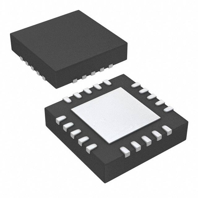


 工商网监
湘ICP备2023018690号
工商网监
湘ICP备2023018690号
