TPS561201, TPS561208
TPS561201,
TPS561208
ZHCSG73A – APRIL 2017 –
REVISED SEPTEMBER
2020
ZHCSG73A – APRIL 2017 – REVISED SEPTEMBER 2020
www.ti.com.cn
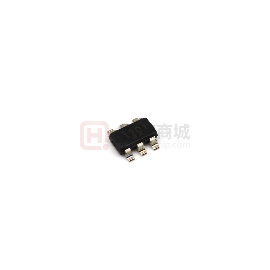
采用 6 引脚 SOT-23 封装的 TPS56120x 4.5V 至 17V 输入、1A 同步降压稳压器
1 特性
• TPS561201 和 TPS561208 1A 转换器集成了
140mΩ 和 84mΩ FET
• {1}D-CAP2{2} 模式控制,用于快速瞬态响应
• 输入电压范围:4.5V 至 17V
• 输出电压范围:0.76V 至 7V
• 脉冲跳跃模式 (TPS561201) 或持续电流模式
(TPS561208)
• 580kHz 开关频率
• 低关断电流(低于 10µA)
• 2% 反馈电压精度 (25°C)
• 从预偏置输出电压启动
• 逐周期过流限制
• 断续模式过流保护
• 非锁存欠压保护 (UVP) 和热关断 (TSD) 保护
• 固定软启动:1.0ms
• 使用 TPS56120x 并借助 WEBENCH® 电源设计器
创建定制设计方案
• 数字机顶盒 (STB)
• 监控
3 说明
TPS561201 和 TPS561208 是采用 SOT-23 封装的简
单易用型 1A 同步降压转换器。
此器件被优化为使用尽可能少的外部组件即可运行,并
且可以实现低待机电流。
这些开关模式电源 (SMPS) 器件采用 D-CAP2 模式控
制,从而提供快速瞬态响应,并且在无需外部补偿组件
的情况下支持专用聚合物等低等效串联电阻 (ESR) 输
出电容器以及超低 ESR 陶瓷电容器。
TPS561201 可在脉冲跳跃模式下运行,从而能在轻载
运行期间保持高效率。TPS561201 和 TPS561208 可
提供 6 引脚 1.6 × 2.9 (mm) SOT (DDC) 封装,额定结
温范围为 –40°C 至 125°C。
器件信息
器件型号
TPS561201
TPS561208
2 应用
• 数字电视电源
• 高清蓝光™光盘播放器
• 网络家庭终端设备
(1)
(1)
封装
SOT (6)
封装尺寸(标称值)
1.60mm x 2.90mm
如需了解所有可用封装,请参阅数据表末尾的可订购产品附
录。
100%
90%
TPS561201
GND
2
VOUT
COUT
3
VIN
VBST
SW
EN
VIN
VFB
80%
70%
6
5
EN
Efficiency
1
4
VOUT
60%
50%
40%
30%
Vout = 1.05 V
Vout = 1.5 V
Vout = 3.3 V
Vout = 5 V
20%
CIN
10%
0
0.001
简化原理图
0.01
0.1
Output Current (A)
1
D001
TPS561201 效率
本文档旨在为方便起见,提供有关
TI 产品中文版本的信息,以确认产品的概要。有关适用的官方英文版本的最新信息,请访问
Copyright
© 2021 Texas Instruments Incorporated
Submit Document Feedback
www.ti.com,其内容始终优先。TI 不保证翻译的准确性和有效性。在实际设计之前,请务必参考最新版本的英文版本。
Product Folder Links: TPS561201 TPS561208
English Data Sheet: SLVSC95
1
�TPS561201, TPS561208
www.ti.com.cn
ZHCSG73A – APRIL 2017 – REVISED SEPTEMBER 2020
Table of Contents
1 特性................................................................................... 1
2 应用................................................................................... 1
3 说明................................................................................... 1
4 Revision History.............................................................. 2
5 Pin Configuration and Functions...................................3
Pin Functions.................................................................... 3
6 Specifications.................................................................. 4
6.1 Absolute Maximum Ratings........................................ 4
6.2 ESD Ratings............................................................... 4
6.3 Recommended Operating Conditions.........................4
6.4 Thermal Information....................................................4
6.5 Electrical Characteristics.............................................5
6.6 Typical Characteristics................................................ 6
7 Detailed Description........................................................9
7.1 Overview..................................................................... 9
7.2 Functional Block Diagram........................................... 9
7.3 Feature Description.....................................................9
7.4 Device Functional Modes..........................................10
8 Application and Implementation.................................. 12
8.1 Application Information............................................. 12
8.2 Typical Application.................................................... 12
9 Power Supply Recommendations................................18
10 Layout...........................................................................19
10.1 Layout Guidelines................................................... 19
10.2 Layout Example...................................................... 19
11 Device and Documentation Support..........................20
11.1 Device Support........................................................20
11.2 Receiving Notification of Documentation Updates.. 20
11.3 Support Resources................................................. 20
11.4 Trademarks............................................................. 20
11.5 Electrostatic Discharge Caution.............................. 20
11.6 Glossary.................................................................. 20
12 Mechanical, Packaging, and Orderable
Information.................................................................... 20
4 Revision History
Changes from Revision * (April 2017) to Revision A (September 2020)
Page
• 更新了整个文档的表、图和交叉参考的编号格式................................................................................................ 1
• Replaced 图 6-5 and 图 6-6 ............................................................................................................................... 6
2
Submit Document Feedback
Copyright © 2021 Texas Instruments Incorporated
Product Folder Links: TPS561201 TPS561208
�TPS561201, TPS561208
www.ti.com.cn
ZHCSG73A – APRIL 2017 – REVISED SEPTEMBER 2020
5 Pin Configuration and Functions
1
GND
2
SW
3
VIN
TPS561201
VBST
6
EN
5
VFB
4
图 5-1. 6-Pin SOTDDC Package (Top View)
Pin Functions
PIN
NAME
DESCRIPTION
NO.
GND
1
Ground pin source terminal of low-side power NFET as well as the ground terminal for controller circuit.
Connect sensitive VFB to this GND at a single point.
SW
2
Switch node connection between high-side NFET and low-side NFET
VIN
3
Input voltage supply pin. The drain terminal of high-side power NFET
VFB
4
Converter feedback input. Connect to output voltage with feedback resistor divider.
EN
5
Enable input control. Active high and must be pulled up to enable the device.
VBST
6
Supply input for the high-side NFET gate drive circuit. Connect 0.1-µF capacitor between VBST and SW pins.
Submit Document Feedback
Copyright © 2021 Texas Instruments Incorporated
Product Folder Links: TPS561201 TPS561208
3
�TPS561201, TPS561208
www.ti.com.cn
ZHCSG73A – APRIL 2017 – REVISED SEPTEMBER 2020
6 Specifications
6.1 Absolute Maximum Ratings
over operating free-air temperature range (unless otherwise noted)(1)
Input voltage
MIN
MAX
UNIT
VIN, EN
–0.3
19
V
VBST
–0.3
25
V
VBST (10-ns transient)
–0.3
27
V
VBST (vs SW)
–0.3
6.5
V
VFB
–0.3
6.5
V
SW
–2
19
V
–3.5
21
V
Operating junction temperature, TJ
–40
150
°C
Storage temperature, Tstg
–55
150
°C
SW (10 ns transient)
(1)
Stresses beyond those listed under Absolute Maximum Ratings may cause permanent damage to the device. These are stress ratings
only, which do not imply functional operation of the device at these or any other conditions beyond those indicated under
Recommended Operating Conditions. Exposure to absolute-maximum-rated conditions for extended periods may affect device
reliability.
6.2 ESD Ratings
VALUE
V(ESD)
(1)
(2)
Electrostatic
discharge
Human-body model (HBM), per ANSI/ESDA/JEDEC JS-001(1)
±3000
Charged-device model (CDM), per JEDEC specification JESD22-C101(2)
±1500
UNIT
V
JEDEC document JEP155 states that 500-V HBM allows safe manufacturing with a standard ESD control process.
JEDEC document JEP157 states that 250-V CDM allows safe manufacturing with a standard ESD control process.
6.3 Recommended Operating Conditions
over operating free-air temperature range (unless otherwise noted)
MIN
VIN
Supply input voltage
VI
Input voltage
TJ
MAX
4.5
17
VBST
–0.1
23
VBST (10-ns transient)
–0.1
26
VBST(vs SW)
–0.1
6.0
EN
–0.1
17
VFB
–0.1
5.5
SW
–1.8
17
SW (10 ns transient)
–3.5
20
–40
125
Operating junction temperature
UNIT
V
V
°C
6.4 Thermal Information
THERMAL METRIC(1)
TPS561201 and
TPS561208
DDC (SOT)
UNIT
6 PINS
4
RθJA
Junction-to-ambient thermal resistance
90.8
°C/W
RθJC(top)
Junction-to-case (top) thermal resistance
42.3
°C/W
RθJB
Junction-to-board thermal resistance
16.3
°C/W
Submit Document Feedback
Copyright © 2021 Texas Instruments Incorporated
Product Folder Links: TPS561201 TPS561208
�TPS561201, TPS561208
www.ti.com.cn
ZHCSG73A – APRIL 2017 – REVISED SEPTEMBER 2020
TPS561201 and
TPS561208
THERMAL METRIC(1)
UNIT
DDC (SOT)
6 PINS
ψJT
Junction-to-top characterization parameter
2.6
°C/W
ψJB
Junction-to-board characterization parameter
16.3
°C/W
(1)
For more information about traditional and new thermal metrics, see the Semiconductor and IC Package Thermal Metrics application
report, SPRA953.
6.5 Electrical Characteristics
TJ = –40°C to 125°C, V = 12 V (unless otherwise noted)
PARAMETER
TEST CONDITIONS
MIN
TYP
MAX
UNIT
SUPPLY CURRENT
IVIN
Operating – non-switching
supply current
VIN current, EN = 5 V, VFB =
0.8 V
IVINSDN
Shutdown supply current
VIN current, EN = 0 V
TPS561201
380
520
TPS561208
590
750
1
10
µA
µA
LOGIC THRESHOLD
VENH
EN high-level input voltage
EN
VENL
EN low-level input voltage
EN
REN
EN pin resistance to GND
VEN = 12 V
1.6
V
0.8
V
900
kΩ
225
400
749
768
787
mV
0
±0.1
µA
VFB VOLTAGE AND DISCHARGE RESISTANCE
VFB threshold voltage
VO = 1.05 V, IO = 10 mA, Eco-mode™ operation
VFBTH
VFB threshold voltage
VO = 1.05 V, continuous mode operation
IVFB
VFB input current
VFB = 0.8 V
RDS(on)h
High-side switch resistance
TA = 25°C, VBST – SW = 5.5 V
RDS(on)l
Low-side switch resistance
TA = 25°C
774
mV
MOSFET
140
mΩ
84
mΩ
CURRENT LIMIT
Iocl
Current limit
DC current, VOUT = 1.05 V, L1 = 2.2 µH
1.2
1.6
2.0
A
THERMAL SHUTDOWN
TSDN
Thermal shutdown threshold(1)
Shutdown temperature
Hysteresis
160
°C
25
ON-TIME TIMER CONTROL
tOFF(MIN)
Minimum off time
VFB = 0.5 V
220
310
ns
Soft-start time
Internal soft-start time
1.0
ms
Switching frequency
VIN = 12 V, VO = 1.05 V, FCCM mode
580
kHz
SOFT START
tss
Frequency
Fsw
OUTPUT UNDERVOLTAGE AND OVERVOLTAGE PROTECTION
VUVP
Output UVP threshold
THICCUP_WAI
Hiccup wait time
1.8
ms
Hiccup time before restart
15
ms
T
THICCUP_RE
Hiccup detect (H > L)
65%
UVLO
Submit Document Feedback
Copyright © 2021 Texas Instruments Incorporated
Product Folder Links: TPS561201 TPS561208
5
�TPS561201, TPS561208
www.ti.com.cn
ZHCSG73A – APRIL 2017 – REVISED SEPTEMBER 2020
TJ = –40°C to 125°C, V = 12 V (unless otherwise noted)
PARAMETER
TEST CONDITIONS
MIN
Wake up VIN voltage
UVLO
UVLO threshold
Shut down VIN voltage
3.3
Hysteresis VIN voltage
(1)
TYP
MAX
4.0
4.3
3.6
UNIT
V
0.4
Not production tested
6.6 Typical Characteristics
VIN = 12 V (unless otherwise noted)
0.762
0.45
FB Voltage (V)
Buck Quiescent Current (mA)
0.5
0.4
0.761
0.76
0.35
0.3
-50
-20
10
40
70
TJ - Junction Temperature (qC)
100
0.759
-50
130
-20
10
40
70
TJ - Junction Temperature (qC)
100
图 6-1. TPS561201 Supply Current vs Junction
Temperature
130
D002
D001
图 6-2. VFB Voltage vs Junction Temperature
1.45
1.23
EN Pin UVLO - High (V)
EN Pin UVLO - Low (V)
1.2
1.17
1.14
1.11
1.08
1.42
1.39
1.36
1.33
1.05
1.02
-50
-20
10
40
70
TJ - Junction Temperature (qC)
100
130
-20
D004
图 6-3. EN Pin UVLO Low Voltage vs Junction
Temperature
6
1.3
-50
10
40
70
TJ - Junction Temperature (qC)
100
130
D003
图 6-4. EN Pin UVLO High Voltage vs Junction
Temperature
Submit Document Feedback
Copyright © 2021 Texas Instruments Incorporated
Product Folder Links: TPS561201 TPS561208
�TPS561201, TPS561208
ZHCSG73A – APRIL 2017 – REVISED SEPTEMBER 2020
250
130
230
120
210
Low Side Rds_on (mŸ)
High Side Rds_on (mŸ)
www.ti.com.cn
190
170
150
130
110
110
100
90
80
70
60
90
50
70
±50
10
±20
40
70
100
Junction Temperature (ƒC)
500
Switching Frequency (KHz)
600
560
540
Vout = 1.05 V
Vout = 3.3 V
Vout = 5 V
500
4
6
8
10
12
Input Voltage (V)
14
16
50
70
90
110
130
C006
300
200
100
0
0.001
18
D007
0.01
0.1
Output Current (A)
1
D009
VIN = 12 V
图 6-7. TPS561208 Switching Frequency vs Input
Voltage
图 6-8. TPS561201 Switching Frequency vs Output
Current
100%
100%
90%
90%
80%
80%
70%
70%
60%
60%
Efficiency
Efficiency
30
400
Iout = 10 mA
50%
40%
30%
50%
40%
30%
Vin = 5 V
Vin = 9 V
Vin = 12 V
Vin = 15 V
20%
10%
0
0.001
10
图 6-6. Low-Side Rds-on vs Junction Temperature
600
580
±10
Junction Temperature (ƒC)
620
520
±30
C005
图 6-5. High-Side Rds-on vs Junction Temperature
Switching Frequency (KHz)
±50
130
0.01
0.1
Output Current (A)
Vin = 5 V
Vin = 9 V
Vin = 12 V
Vin = 15 V
20%
10%
1
0
0.001
D010
0.01
0.1
Output Current (A)
1
D011
图 6-9. TPS561201 VOUT = 1.05 V, Efficiency, L = 2.2 图 6-10. TPS561201 VOUT = 1.5 V, Efficiency, L = 2.2
µH
µH
Submit Document Feedback
Copyright © 2021 Texas Instruments Incorporated
Product Folder Links: TPS561201 TPS561208
7
�TPS561201, TPS561208
www.ti.com.cn
100%
100%
90%
90%
80%
80%
70%
70%
60%
60%
Efficiency
Efficiency
ZHCSG73A – APRIL 2017 – REVISED SEPTEMBER 2020
50%
40%
30%
40%
30%
Vin = 5 V
Vin = 9 V
Vin = 12 V
Vin = 15 V
20%
10%
0
0.001
50%
0.01
0.1
Output Current (A)
20%
Vin = 9 V
Vin = 12 V
Vin = 15 V
10%
0
0.001
1
D012
图 6-11. TPS561201 VOUT = 3.3 V, Efficiency, L = 3.3
µH
0.01
0.1
Output Current (A)
1
D013
图 6-12. TPS561201 VOUT = 5 V, Efficiency, L = 4.7
µH
100%
1
90%
80%
0.8
Efficiency
Efficiency
70%
0.6
0.4
60%
50%
40%
30%
Vin = 5 V
Vin = 9 V
Vin = 12 V
Vin = 15 V
0.2
0
0.001
0.01
0.1
Output Current (A)
10%
D014
90%
80%
80%
70%
70%
60%
60%
Efficiency
Efficiency
100%
90%
50%
40%
0.01
0.1
Output Current (A)
1
D015
图 6-14. TPS561208 VOUT = 1.5 V, Efficiency, L = 2.2
µH
100%
50%
40%
30%
30%
Vin = 5 V
Vin = 9 V
Vin = 12 V
Vin = 15 V
20%
10%
0.01
0.1
Output Current (A)
20%
Vin = 9 V
Vin = 12 V
Vin = 15 V
10%
1
0
0.001
D016
图 6-15. TPS561208 VOUT = 3.3 V, Efficiency, L = 3.3
µH
8
0
0.001
1
图 6-13. TPS561208 VOUT = 1.05 V, Efficiency, L =
2.2 µH
0
0.001
Vin = 5 V
Vin = 9 V
Vin = 12 V
Vin = 15 V
20%
0.01
0.1
Output Current (A)
1
D017
图 6-16. TPS561208 VOUT = 5 V, Efficiency, L = 4.7
µH
Submit Document Feedback
Copyright © 2021 Texas Instruments Incorporated
Product Folder Links: TPS561201 TPS561208
�TPS561201, TPS561208
www.ti.com.cn
ZHCSG73A – APRIL 2017 – REVISED SEPTEMBER 2020
7 Detailed Description
7.1 Overview
The TPS561201 and TPS561208 are 1-A synchronous step-down converters. The proprietary D-CAP2 mode
control supports low-ESR output capacitors such as specialty polymer capacitors and multi-layer ceramic
capacitors without complex external compensation circuits. The fast transient response of D-CAP2 mode control
can reduce the output capacitance required to meet a specific level of performance.
7.2 Functional Block Diagram
EN 5
VUVP
VOVP
VFB
+
UVP
Hiccup
Ref
Soft Start
SS
6
VBST
2
SW
1
GND
UVLO
4
Voltage
Reference
VIN
VREG5
Regulator
+
OVP
3
PWM
+
+
HS
Control Logic
Ton
One-Shot
XCON
VREG5
TSD
LS
OCL
threshold
OCL
+
+
ZC
7.3 Feature Description
7.3.1 Adaptive On-Time Control and PWM Operation
The main control loop of the TPS561201 is adaptive on-time pulse width modulation (PWM) controller that
supports a proprietary D-CAP2 mode control. The D-CAP2 mode control combines adaptive on-time control with
an internal compensation circuit for pseudo-fixed frequency and low external component count configuration with
both low ESR and ceramic output capacitors. It is stable even with virtually no ripple at the output.
At the beginning of each cycle, the high-side MOSFET is turned on. This MOSFET is turned off after internal one
shot timer expires. This one shot duration is set proportional to the converter input voltage, VIN, and inversely
proportional to the output voltage, VO, to maintain a pseudo-fixed frequency over the input voltage range, hence
it is called adaptive on-time control. The one-shot timer is reset and the high-side MOSFET is turned on again
when the feedback voltage falls below the reference voltage. An internal ramp is added to reference voltage to
simulate output ripple, eliminating the need for ESR induced output ripple from D-CAP2 mode control.
7.3.2 Pulse Skip Control (TPS561201)
The TPS561201 and TPS561208 are designed with Advanced Eco-mode to maintain high light load efficiency.
As the output current decreases from heavy load condition, the inductor current is also reduced and eventually
comes to point that the rippled valley touches zero level, which is the boundary between continuous conduction
Submit Document Feedback
Copyright © 2021 Texas Instruments Incorporated
Product Folder Links: TPS561201 TPS561208
9
�TPS561201, TPS561208
www.ti.com.cn
ZHCSG73A – APRIL 2017 – REVISED SEPTEMBER 2020
and discontinuous conduction modes. The rectifying MOSFET is turned off when the zero inductor current is
detected. As the load current further decreases, the converter runs into discontinuous conduction mode. The ontime is kept almost the same as it was in continuous conduction mode so that it takes longer time to discharge
the output capacitor with smaller load current to the level of the reference voltage. This makes the switching
frequency lower and proportional to the load current, and keeps the light load efficiency high. The transition point
to the light load operation IOUT(LL) current can be calculated in 方程式 1.
IOUT(LL) =
(V - VOUT ) ´ VOUT
1
´ IN
2 ´ L ´ fSW
VIN
(1)
7.3.3 Soft Start and Pre-Biased Soft Start
The TPS561201 and TPS561208 have an internal 1.0-ms soft start. When the EN pin becomes high, the internal
soft-start function begins ramping up the reference voltage to the PWM comparator. If the output capacitor is prebiased at start-up, the devices initiate switching and start ramping up only after the internal reference voltage
becomes greater than the feedback voltage VFB. This scheme ensures that the converters ramp up smoothly
into regulation point.
7.3.4 Current Protection
The output overcurrent limit (OCL) is implemented using a cycle-by-cycle valley detect control circuit. The switch
current is monitored during the OFF state by measuring the low-side FET drain to source voltage. This voltage is
proportional to the switch current. To improve accuracy, the voltage sensing is temperature compensated.
During the on-time of the high-side FET switch, the switch current increases at a linear rate determined by Vin,
Vout, the on-time, and the output inductor value. During the on-time of the low-side FET switch, this current
decreases linearly. The average value of the switch current is the load current Iout. If the monitored current is
above the OCL level, the converter maintains low-side FET on and delays the creation of a new set pulse, even
the voltage feedback loop requires one, until the current level becomes OCL level or lower. In subsequent
switching cycles, the on-time is set to a fixed value and the current is monitored in the same manner.
There are some important considerations for this type of over-current protection. The load current is higher than
the overcurrent threshold by one half of the peak-to-peak inductor ripple current. Also, when the current is being
limited, the output voltage tends to fall as the demanded load current can be higher than the current available
from the converter. This can cause the output voltage to fall. When the VFB voltage falls below the UVP
threshold voltage, the UVP comparator detects it. And then, the device will shut down after the UVP delay time
(typically 24 µs) and restart after the hiccup time (typically 15 ms).
When the overcurrent condition is removed, the output voltage returns to the regulated value.
7.3.5 Undervoltage Lockout (UVLO) Protection
UVLO protection monitors the internal regulator voltage. When the voltage is lower than UVLO threshold voltage,
the device is shut off. This protection is non-latching.
7.3.6 Thermal Shutdown
The device monitors the temperature of itself. If the temperature exceeds the threshold value (typically 160°C),
the device is shut off. This is a non-latch protection.
7.4 Device Functional Modes
7.4.1 Normal Operation
When the input voltage is above the UVLO threshold and the EN voltage is above the enable threshold, the
TPS561208 can operate in their normal switching modes. Normal continuous conduction mode (CCM) occurs
when the minimum switch current is above 0 A. In CCM, the TPS561208 operates at a quasi-fixed frequency of
580 kHz.
7.4.2 Eco-mode Operation
When the TPS561201 and TPS561208 are in the normal CCM operating mode and the switch current falls to 0
A, the TPS561201 begins operating in pulse skipping Eco-mode. Each switching cycle is followed by a period of
10
Submit Document Feedback
Copyright © 2021 Texas Instruments Incorporated
Product Folder Links: TPS561201 TPS561208
�TPS561201, TPS561208
www.ti.com.cn
ZHCSG73A – APRIL 2017 – REVISED SEPTEMBER 2020
energy saving sleep time. The sleep time ends when the VFB voltage falls below the Eco-mode threshold
voltage. As the output current decreases, the perceived time between switching pulses increases.
7.4.3 Standby Operation
When the TPS561201 and TPS561208 are operating in either normal CCM or Eco-mode, they can be placed in
standby by asserting the EN pin low.
Submit Document Feedback
Copyright © 2021 Texas Instruments Incorporated
Product Folder Links: TPS561201 TPS561208
11
�TPS561201, TPS561208
www.ti.com.cn
ZHCSG73A – APRIL 2017 – REVISED SEPTEMBER 2020
8 Application and Implementation
Note
Information in the following applications sections is not part of the TI component specification, and TI
does not warrant its accuracy or completeness. TI’s customers are responsible for determining
suitability of components for their purposes. Customers should validate and test their design
implementation to confirm system functionality.
8.1 Application Information
The devices are typical step-down DC-DC converters. It typically uses to convert a higher dc voltage to a lower
dc voltage with a maximum available output current of 1 A. The following design procedure can be used to select
component values for the TPS561201 and TPS561208. Alternately, the WEBENCH® software can be used to
generate a complete design. The WEBENCH software uses an iterative design procedure and accesses a
comprehensive database of components when generating a design. This section presents a simplified
discussion of the design process.
8.2 Typical Application
The application schematic in 图 8-1 was developed to meet the previous requirements. This circuit is available
as the evaluation module (EVM). The sections provide the design procedure.
图 8-1 shows the TPS561201 and TPS561208 4.5-V to 17-V Input, 1.05-V output converter schematics.
C7 0.1 uF
6
1
GND
VOUT = 1.05 V / 1 A L1
2
VOUT
VBST
R3 10.0 k
5
SW
EN
VIN
VFB
EN
2.2 uH
C9
3
C8
4
VOUT
R1 3.09 k
22 uF 22 uF
R2
10 k
1
C1
C2
C3
C4
Not Installed 1
10 uF 10 uF 0.1 uF
VIN
VIN = 4.5 to 17 V
1
图 8-1. TPS561201 and TPS561208 1.05-V/1-A Reference Design
8.2.1 Design Requirements
表 8-1 shows the design parameters.
表 8-1. Design Parameters
PARAMETER
Input voltage range
Output voltage
Transient response, 1-A load step
12
EXAMPLE VALUE
4.5 to 17 V
1.05 V
ΔVout = ±5%
Input ripple voltage
400 mV
Output ripple voltage
30 mV
Output current rating
1A
Operating frequency
580 kHz
Submit Document Feedback
Copyright © 2021 Texas Instruments Incorporated
Product Folder Links: TPS561201 TPS561208
�TPS561201, TPS561208
www.ti.com.cn
ZHCSG73A – APRIL 2017 – REVISED SEPTEMBER 2020
8.2.2 Detailed Design Procedure
8.2.2.1 Custom Design With WEBENCH® Tools
Click here to create a custom design using the TPS56120x device with the WEBENCH® Power Designer.
1. Start by entering the input voltage (VIN), output voltage (VOUT), and output current (IOUT) requirements.
2. Optimize the design for key parameters such as efficiency, footprint, and cost using the optimizer dial.
3. Compare the generated design with other possible solutions from Texas Instruments.
The WEBENCH Power Designer provides a customized schematic along with a list of materials with real-time
pricing and component availability.
In most cases, these actions are available:
• Run electrical simulations to see important waveforms and circuit performance
• Run thermal simulations to understand board thermal performance
• Export customized schematic and layout into popular CAD formats
• Print PDF reports for the design, and share the design with colleagues
Get more information about WEBENCH tools at www.ti.com/WEBENCH.
8.2.2.2 Output Voltage Resistors Selection
The output voltage is set with a resistor divider from the output node to the VFB pin. TI recommends to use 1%
tolerance or better divider resistors. Start by using 方程式 2 to calculate VOUT.
To improve efficiency at very light loads, consider using larger value resistors. Too high of resistance will be more
susceptible to noise and voltage errors from the VFB input current will be more noticeable.
R1 ö
æ
VOUT = 0.768 ´ ç 1 +
÷
R2
è
ø
(2)
8.2.2.3 Output Filter Selection
The LC filter used as the output filter has double pole at:
FP =
1
2p LOUT ´ COUT
(3)
At low frequencies, the overall loop gain is set by the output set-point resistor divider network and the internal
gain of the device. The low frequency phase is 180 degrees. At the output filter pole frequency, the gain rolls off
at a –40 dB per decade rate and the phase drops rapidly. D-CAP2 introduces a high frequency zero that
reduces the gain roll off to –20 dB per decade and increases the phase to 90 degrees one decade above the
zero frequency. The inductor and capacitor for the output filter must be selected so that the double pole of 方程
式 3 is located below the high frequency zero but close enough that the phase boost provided be the high
frequency zero provides adequate phase margin for a stable circuit. To meet this requirement use the values
recommended in 表 8-2.
表 8-2. Recommended Component Values
L1 (µH)
OUTPUT VOLTAGE
(V)
R1
(kΩ)
R2
(kΩ)
MIN
TYP
MAX
C8 + C9
(µF)
1
3.09
10.0
2.2
2.2
4.7
20 to 68
1.05
3.74
10.0
2.2
2.2
4.7
20 to 68
1.2
5.76
10.0
2.2
2.2
4.7
20 to 68
1.5
9.53
10.0
2.2
2.2
4.7
20 to 68
1.8
13.7
10.0
2.2
2.2
4.7
20 to 68
2.5
22.6
10.0
3.3
3.3
4.7
20 to 68
Submit Document Feedback
Copyright © 2021 Texas Instruments Incorporated
Product Folder Links: TPS561201 TPS561208
13
�TPS561201, TPS561208
www.ti.com.cn
ZHCSG73A – APRIL 2017 – REVISED SEPTEMBER 2020
表 8-2. Recommended Component Values (continued)
L1 (µH)
OUTPUT VOLTAGE
(V)
R1
(kΩ)
R2
(kΩ)
MIN
TYP
MAX
C8 + C9
(µF)
3.3
33.2
10.0
3.3
3.3
4.7
20 to 68
5
54.9
10.0
3.3
4.7
4.7
20 to 68
6.5
75
10.0
3.3
4.7
4.7
20 to 68
The inductor peak-to-peak ripple current, peak current and RMS current are calculated using 方程式 4, 方程式 5,
and 方程式 6. The inductor saturation current rating must be greater than the calculated peak current and the
RMS or heating current rating must be greater than the calculated RMS current.
Use 580 kHz for fSW. Make sure the chosen inductor is rated for the peak current of 方程式 5 and the RMS
current of 方程式 6.
IlP -P =
VIN(MAX) - VOUT
VOUT
´
VIN(MAX)
LO ´ fSW
IlPEAK = IO +
(4)
IlP -P
2
ILO(RMS) = IO2 +
(5)
1
IlP -P2
12
(6)
For this design example, the calculated peak current is 1.69 A and the calculated RMS current is 1.11 A. The
inductor used is a WE 744311330 with a peak current rating of 11 A and an RMS current rating of 6.5 A.
The capacitor value and ESR determines the amount of output voltage ripple. The TPS561201 and TPS561208
are intended for use with ceramic or other low-ESR capacitors. Recommended values range from 20 µF to 68
µF. Use 方程式 7 to determine the required RMS current rating for the output capacitor.
ICO(RMS) =
VOUT ´ (VIN - VOUT )
12 ´ VIN ´ LO ´ fSW
(7)
For this design, two TDK C3216X5R0J226M 22-µF output capacitors are used. The typical ESR is 2 mΩ each.
The calculated RMS current is 0.286 A.
8.2.2.4 Input Capacitor Selection
The TPS561201 and TPS561208 require an input decoupling capacitor and a bulk capacitor is needed
depending on the application. TI recommends a ceramic capacitor over 10 µF for the decoupling capacitor. An
additional 0.1-µF capacitor (C3) from pin 3 to ground is optional to provide additional high frequency filtering.
The capacitor voltage rating needs to be greater than the maximum input voltage.
8.2.2.5 Bootstrap Capacitor Selection
A 0.1-µF ceramic capacitor must be connected between the VBST to SW pin for proper operation. TI
recommends to use a ceramic capacitor.
14
Submit Document Feedback
Copyright © 2021 Texas Instruments Incorporated
Product Folder Links: TPS561201 TPS561208
�TPS561201, TPS561208
www.ti.com.cn
ZHCSG73A – APRIL 2017 – REVISED SEPTEMBER 2020
8.2.3 Application Curves
3.00%
3.00%
TPS561201
TPS561208
2.00%
Output Voltage (V)
Output Voltage (V)
2.00%
1.00%
0.00
-1.00%
1.00%
0.00
-1.00%
-2.00%
-2.00%
-3.00%
-3.00%
0
0.2
0.4
0.6
Output Current (A)
0.8
0
1
0.2
D018
图 8-2. Load Regulation VIN = 5 V
0.4
0.6
Output Current (A)
0.8
1
D019
D018
图 8-3. Load Regulation VIN = 12 V
100%
1.07
TPS561201
TPS561208
1.065
90%
80%
70%
1.06
Efficiency
Output Voltage (V)
TPS561201
TPS561208
1.055
1.05
60%
50%
40%
30%
Vin = 5 V
Vin = 9 V
Vin = 12 V
Vin = 15 V
20%
1.045
10%
1.04
4
6
8
TPS56201 IOUT = 0.5 A
10
12
Input Voltage (V)
14
16
18
0
0.001
0.01
0.1
Output Current (A)
D020
1
D021
TPS56208 IOUT = 10 mA
图 8-4. Line Regulation
图 8-5. TPS561201 VOUT = 1.05 V, Efficiency L = 2.2
µH
50 mV/div
100 mV/div
5 V/div
5 V/div
1 A/div
500 mA/div
4 us/div
1 us/div
图 8-6. TPS561201 Input Voltage Ripple
图 8-7. TPS561201 Output Voltage Ripple, IOUT = 10
mA
Submit Document Feedback
Copyright © 2021 Texas Instruments Incorporated
Product Folder Links: TPS561201 TPS561208
15
�TPS561201, TPS561208
www.ti.com.cn
ZHCSG73A – APRIL 2017 – REVISED SEPTEMBER 2020
20 mV/div
20 mV/div
5 V/div
5 V/div
500 mA/div
500 mA/div
1 us/div
1 us/div
图 8-8. TPS561201 Output Voltage Ripple, IOUT =
0.25 A
图 8-9. TPS561201 Output Voltage Ripple, IOUT = 1
A
50 mV/div
20 mV/div
500 mA/div
5 V/div
100 us/div
1 us/div
图 8-10. TPS561208 Output Voltage Ripple, IOUT = 0
A
50 mV/div
图 8-11. TPS561201 Transient Response, 0.1 to 1 A
50 mV/div
500 mA/div
500 mA/div
100 us/div
100 us/div
图 8-12. TPS561201 Transient Response, 0.5 to 1.5
A
16
图 8-13. TPS561208 Transient Response 0.1 to 1 A
Submit Document Feedback
Copyright © 2021 Texas Instruments Incorporated
Product Folder Links: TPS561201 TPS561208
�TPS561201, TPS561208
www.ti.com.cn
ZHCSG73A – APRIL 2017 – REVISED SEPTEMBER 2020
5 V/div
5 V/div
5 V/div
5 V/div
500 mV/div
500 mV/div
1 ms/div
2 ms/div
图 8-14. TPS561201 Start-Up Relative to VI
图 8-15. TPS561201 Start-Up Relative to EN
5 V/div
5 V/div
5 V/div
5 V/div
500 mV/div
500 mV/div
100 us/div
10 ms/div
图 8-16. TPS561201 Shutdown Relative to VI
图 8-17. TPS561201 Shutdown Relative to EN
Submit Document Feedback
Copyright © 2021 Texas Instruments Incorporated
Product Folder Links: TPS561201 TPS561208
17
�TPS561201, TPS561208
ZHCSG73A – APRIL 2017 – REVISED SEPTEMBER 2020
www.ti.com.cn
9 Power Supply Recommendations
The TPS561201 and TPS561208 are designed to operate from input supply voltage in the range of 4.5 V to 17
V. Buck converters require the input voltage to be higher than the output voltage for proper operation. The
maximum recommended operating duty cycle is 75%. Using that criteria, the minimum recommended input
voltage is VO / 0.75.
18
Submit Document Feedback
Copyright © 2021 Texas Instruments Incorporated
Product Folder Links: TPS561201 TPS561208
�TPS561201, TPS561208
www.ti.com.cn
ZHCSG73A – APRIL 2017 – REVISED SEPTEMBER 2020
10 Layout
10.1 Layout Guidelines
1. VIN and GND traces should be as wide as possible to reduce trace impedance. The wide areas are also of
advantage from the view point of heat dissipation.
2. The input capacitor and output capacitor should be placed as close to the device as possible to minimize
trace impedance.
3. Provide sufficient vias for the input capacitor and output capacitor.
4. Keep the SW trace as physically short and wide as practical to minimize radiated emissions.
5. Do not allow switching current to flow under the device.
6. A separate VOUT path should be connected to the upper feedback resistor.
7. Make a Kelvin connection to the GND pin for the feedback path.
8. Voltage feedback loop should be placed away from the high-voltage switching trace, and preferably has
ground shield.
9. The trace of the VFB node should be as small as possible to avoid noise coupling.
10.The GND trace between the output capacitor and the GND pin should be as wide as possible to minimize its
trace impedance.
10.2 Layout Example
VOUT
GND
Additional
Vias to the
GND plane
OUTPUT
CAPACITOR
Vias to the
internal SW
node copper
BOOST
CAPACITOR
OUTPUT
INDUCTOR
Vias to the
internal SW
node copper
VIN
GND
VBST
SW
EN
VIN
TO ENABLE
CONTROL
FEEDBACK
RESISTORS
VFB
INPUT BYPAS
CAPACITOR
SW node copper
pour area on internal
or bottom layer
图 10-1. TPS561201 and TPS561208 Layout
Submit Document Feedback
Copyright © 2021 Texas Instruments Incorporated
Product Folder Links: TPS561201 TPS561208
19
�TPS561201, TPS561208
www.ti.com.cn
ZHCSG73A – APRIL 2017 – REVISED SEPTEMBER 2020
11 Device and Documentation Support
11.1 Device Support
11.1.1 Development Support
11.1.1.1 Custom Design With WEBENCH® Tools
Click here to create a custom design using the TPS56120x device with the WEBENCH® Power Designer.
1. Start by entering the input voltage (VIN), output voltage (VOUT), and output current (IOUT) requirements.
2. Optimize the design for key parameters such as efficiency, footprint, and cost using the optimizer dial.
3. Compare the generated design with other possible solutions from Texas Instruments.
The WEBENCH Power Designer provides a customized schematic along with a list of materials with real-time
pricing and component availability.
In most cases, these actions are available:
• Run electrical simulations to see important waveforms and circuit performance
• Run thermal simulations to understand board thermal performance
• Export customized schematic and layout into popular CAD formats
• Print PDF reports for the design, and share the design with colleagues
Get more information about WEBENCH tools at www.ti.com/WEBENCH.
11.2 Receiving Notification of Documentation Updates
To receive notification of documentation updates, navigate to the device product folder on ti.com. Click on
Subscribe to updates to register and receive a weekly digest of any product information that has changed. For
change details, review the revision history included in any revised document.
11.3 Support Resources
TI E2E ™ support forums are an engineer's go-to source for fast, verified answers and design help — straight
from the experts. Search existing answers or ask your own question to get the quick design help you need.
Linked content is provided "AS IS" by the respective contributors. They do not constitute TI specifications and do
not necessarily reflect TI's views; see TI's Terms of Use.
11.4 Trademarks
蓝光™ is a trademark of Blu-ray Disc Association.
Eco-mode™ and TI E2E™ are trademarks of Texas Instruments.
WEBENCH® is a registered trademark of Texas Instruments.
is a registered trademark of Texas Instruments.
所有商标均为其各自所有者的财产。
11.5 Electrostatic Discharge Caution
This integrated circuit can be damaged by ESD. Texas Instruments recommends that all integrated circuits be handled
with appropriate precautions. Failure to observe proper handling and installation procedures can cause damage.
ESD damage can range from subtle performance degradation to complete device failure. Precision integrated circuits may
be more susceptible to damage because very small parametric changes could cause the device not to meet its published
specifications.
11.6 Glossary
TI Glossary
This glossary lists and explains terms, acronyms, and definitions.
12 Mechanical, Packaging, and Orderable Information
The following pages include mechanical, packaging, and orderable information. This information is the most
current data available for the designated devices. This data is subject to change without notice and revision of
this document. For browser-based versions of this data sheet, refer to the left-hand navigation.
20
Submit Document Feedback
Copyright © 2021 Texas Instruments Incorporated
Product Folder Links: TPS561201 TPS561208
�重要声明和免责声明
TI 提供技术和可靠性数据(包括数据表)、设计资源(包括参考设计)、应用或其他设计建议、网络工具、安全信息和其他资源,不保证没
有瑕疵且不做出任何明示或暗示的担保,包括但不限于对适销性、某特定用途方面的适用性或不侵犯任何第三方知识产权的暗示担保。
这些资源可供使用 TI 产品进行设计的熟练开发人员使用。您将独自承担以下全部责任:(1) 针对您的应用选择合适的 TI 产品,(2) 设计、验
证并测试您的应用,(3) 确保您的应用满足相应标准以及任何其他安全、安保或其他要求。这些资源如有变更,恕不另行通知。TI 授权您仅可
将这些资源用于研发本资源所述的 TI 产品的应用。严禁对这些资源进行其他复制或展示。您无权使用任何其他 TI 知识产权或任何第三方知
识产权。您应全额赔偿因在这些资源的使用中对 TI 及其代表造成的任何索赔、损害、成本、损失和债务,TI 对此概不负责。
TI 提供的产品受 TI 的销售条款 () 或 TI.com.cn 上其他适用条款/TI 产品随附的其他适用条款的约束。TI 提供这些资源并不会扩展或以其他方
式更改 TI 针对 TI 产品发布的适用的担保或担保免责声明。IMPORTANT NOTICE
邮寄地址:Texas Instruments, Post Office Box 655303, Dallas, Texas 75265
Copyright © 2020,德州仪器 (TI) 公司
�PACKAGE OPTION ADDENDUM
www.ti.com
10-Dec-2020
PACKAGING INFORMATION
Orderable Device
Status
(1)
Package Type Package Pins Package
Drawing
Qty
Eco Plan
(2)
Lead finish/
Ball material
MSL Peak Temp
Op Temp (°C)
Device Marking
(3)
(4/5)
(6)
TPS561201DDCR
ACTIVE
SOT-23-THIN
DDC
6
3000
RoHS & Green
SN
Level-1-260C-UNLIM
-40 to 125
1201
TPS561201DDCT
ACTIVE
SOT-23-THIN
DDC
6
250
RoHS & Green
SN
Level-1-260C-UNLIM
-40 to 125
1201
TPS561208DDCR
ACTIVE
SOT-23-THIN
DDC
6
3000
RoHS & Green
SN
Level-1-260C-UNLIM
-40 to 85
1208
TPS561208DDCT
ACTIVE
SOT-23-THIN
DDC
6
250
RoHS & Green
SN
Level-1-260C-UNLIM
-40 to 85
1208
(1)
The marketing status values are defined as follows:
ACTIVE: Product device recommended for new designs.
LIFEBUY: TI has announced that the device will be discontinued, and a lifetime-buy period is in effect.
NRND: Not recommended for new designs. Device is in production to support existing customers, but TI does not recommend using this part in a new design.
PREVIEW: Device has been announced but is not in production. Samples may or may not be available.
OBSOLETE: TI has discontinued the production of the device.
(2)
RoHS: TI defines "RoHS" to mean semiconductor products that are compliant with the current EU RoHS requirements for all 10 RoHS substances, including the requirement that RoHS substance
do not exceed 0.1% by weight in homogeneous materials. Where designed to be soldered at high temperatures, "RoHS" products are suitable for use in specified lead-free processes. TI may
reference these types of products as "Pb-Free".
RoHS Exempt: TI defines "RoHS Exempt" to mean products that contain lead but are compliant with EU RoHS pursuant to a specific EU RoHS exemption.
Green: TI defines "Green" to mean the content of Chlorine (Cl) and Bromine (Br) based flame retardants meet JS709B low halogen requirements of


 工商网监
湘ICP备2023018690号
工商网监
湘ICP备2023018690号
