TPS61253A
SLVSDE4D – MARCH 2017 – REVISED JANUARY 2021
TPS61253A 3.8-MHz, 5-V / 4-A Boost Converter in 1.2-mm x 1.3-mm WCSP
1 Features
3 Description
•
•
•
The TPS6125xA device provides a power supply
solution for battery-powered portable applications.
With the input voltage ranging from 2.3 V to 5.5
V, the device supports the applications powered by
the Li-Ion batteries with the extended voltage range.
Different fixed output voltage versions are available of
4.5 V, 4.7 V, 5 V, and 5.2 V. The TPS6125xA supports
up to 1500-mA load current from a battery discharged
as low as 3 V.
•
•
•
•
•
•
•
•
•
•
•
•
•
Wide input voltage range from 2.3 V to 5.5 V
Fixed output voltage: 4.5 / 4.7 / 5.0 / 5.2 V
Two FETs integrated: 35-mΩ LS-FET, 60-mΩ HSFET
IOUT ≥ 1500-mA continuously at VOUT = 5 V and
VIN ≥ 3 V
42-µA quiescent current from input
4-A switching valley current limit
3.8-MHz switching frequency
Selectable auto PFM, forced PWM, and ultrasonic
mode
Support pass-through mode
±2% output voltage accuracy
600-µs soft-start time
Hiccup-mode short protection
Load disconnection during shutdown
Thermal shutdown
Total solution size < 25 mm2
Create a custom design using the TPS61253A
with the WEBENCH® Power Designer
The TPS6125xA operates at typical 3.8-MHz
switching frequency. The TPS6125xA can be flexibly
configured at the Auto PFM mode, forced PWM
mode, or ultrasonic mode. The Auto PFM mode
can benefit with the high efficiency at the light load.
The forced PWM operation can make the switching
frequency be constant crossing the whole load range.
The ultrasonic mode keeps the switching frequency
always larger than 25 kHz at any load condition to
avoid the acoustic noise.
TPS6125xA has a built-in 600-µs soft start to avoid
the inrush current at start-up. When the output is
shorted, the device enters into the hiccup mode and
recovers automatically after the short releases. During
the shutdown, the load is completely disconnected
from the input end with maximum 1.3-μA current
being consumed.
2 Applications
•
•
•
•
•
Smart phones
Portable speaker
USB charging ports
NFC PA supply
Li battery to 5-V power conversion
Device Information
(1)
PART NUMBER
PACKAGE(1)
BODY SIZE (NOM)
TPS61253A
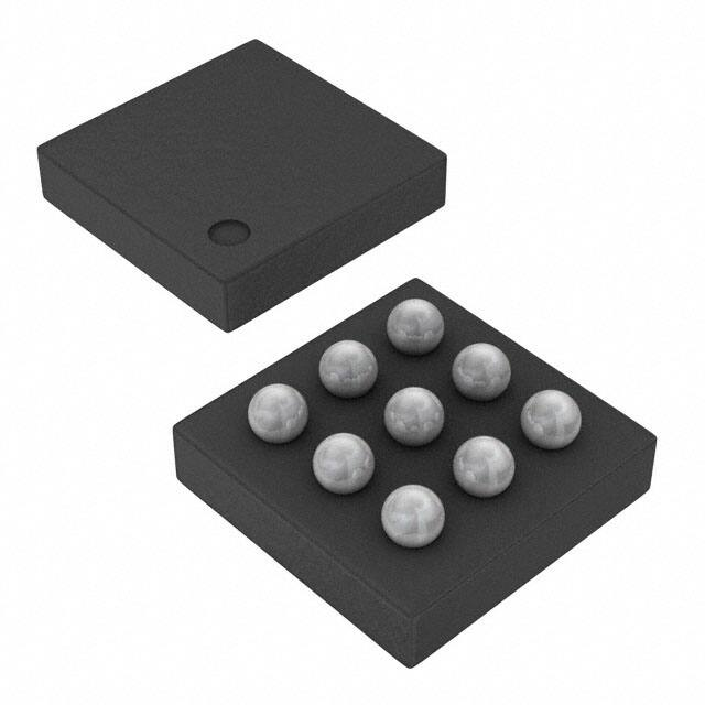
DSBGA (9)
1.2 mm × 1.3 mm
For all available packages, see the orderable addendum at
the end of the data sheet.
L
VOUT
VIN
SW
VOUT
CIN
COUT
VIN
Forced PWM (High)
MODE
Ultrasonic (Floating)
Auto PFM (Low)
OFF
ON
EN
GND
Typical Schematic
An IMPORTANT NOTICE at the end of this data sheet addresses availability, warranty, changes, use in safety-critical applications,
intellectual property matters and other important disclaimers. PRODUCTION DATA.
�TPS61253A
www.ti.com
SLVSDE4D – MARCH 2017 – REVISED JANUARY 2021
Table of Contents
1 Features............................................................................1
2 Applications..................................................................... 1
3 Description.......................................................................1
4 Revision History.............................................................. 2
5 Device Comparison......................................................... 3
6 Pin Configuration and Functions...................................4
7 Specifications.................................................................. 5
7.1 Absolute Maximum Ratings........................................ 5
7.2 ESD Ratings............................................................... 5
7.3 Recommended Operating Conditions.........................5
7.4 Thermal Information....................................................5
7.5 Electrical Characteristics.............................................6
7.6 Timing Requirements.................................................. 7
7.7 Switching Characteristics............................................7
7.8 Typical Characteristics................................................ 8
8 Detailed Description...................................................... 11
8.1 Overview................................................................... 11
8.2 Functional Block Diagram......................................... 12
8.3 Feature Description...................................................12
8.4 Device Functional Modes..........................................14
9 Application and Implementation.................................. 16
9.1 Application Information............................................. 16
9.2 Typical Application ................................................... 16
10 Layout...........................................................................23
10.1 Layout Guidelines................................................... 23
10.2 Layout Example...................................................... 23
10.3 Thermal Considerations..........................................23
11 Device and Documentation Support..........................24
11.1 Device Support .......................................................24
11.2 Documentation Support ......................................... 24
11.3 Receiving Notification of Documentation Updates.. 24
11.4 Support Resources................................................. 24
11.5 Trademarks............................................................. 24
11.6 Electrostatic Discharge Caution.............................. 24
11.7 Glossary.................................................................. 25
4 Revision History
NOTE: Page numbers for previous revisions may differ from page numbers in the current version.
Changes from Revision C (November 2020) to Revision D (January 2021)
Page
• Adding HS FET to the functional block diagram............................................................................................... 12
Changes from Revision B (October 2020) to Revision C (November 2020)
Page
• Removed TPS612532A from the header............................................................................................................1
• Added the device information table.................................................................................................................... 1
Changes from Revision A (December 2017) to Revision B (October 2020)
Page
• Added TPS612532A to TPS6125x data sheet................................................................................................... 1
• Updated the numbering format for tables, figures and cross-references throughout the document...................1
• Updated Device Comparison Table ................................................................................................................... 3
• Changed TPS612531A to TPS612532A in Output Voltage ...............................................................................6
Changes from Revision * (March 2017) to Revision A (December 2017)
Page
• Changed from 5.1 V to 5.2 V in the Specific Features column of the Device Comparison Table for
TPS612592A...................................................................................................................................................... 3
2
Submit Document Feedback
Copyright © 2021 Texas Instruments Incorporated
Product Folder Links: TPS61253A
�TPS61253A
www.ti.com
SLVSDE4D – MARCH 2017 – REVISED JANUARY 2021
5 Device Comparison
(1)
PART NUMBER
OUTPUT VOLTAGE
SW VALLEY
CURRENT LIMIT
(TYP.)
DC START-UP CURRENT
LIMT (TYP.)
SPECIFIC
FEATURES
TPS61253A
5V
4A
1.5 A
Supports output 5
V, up to 1500 mA
TPS612532A
5V
4A
1.5 A
Supports output 5
V, up to 1500
mA with output
discharge function
TPS61254A(1)
4.5 V
2.5 A
0.75 A
Supports output
4.5 V, up to 1000
mA
TPS61255A(1)
4.7 V
4A
1.5 A
Supports output
4.5 V, up to 1500
mA
TPS612561A(1)
5V
2.5 A
0.75 A
Supports output 5
V, up to 1000 mA
TPS61258A(1)
4.5 V
4A
1.5 A
Supports output
4.5 V, up to 1500
mA
TPS612592A(1)
5.2 V
4A
0.75 A
Supports output
5.2 V, up to 1500
mA
TPS612531A(1)
5V
4A
1.5 A
Supports output 5
V, up to 1500 mA
with PFM/PWM
mode only
Preview. Contact TI factory for more information.
Submit Document Feedback
Copyright © 2021 Texas Instruments Incorporated
Product Folder Links: TPS61253A
3
�TPS61253A
www.ti.com
SLVSDE4D – MARCH 2017 – REVISED JANUARY 2021
6 Pin Configuration and Functions
A1
A2
A3
B1
B2
B3
C1
C2
C3
Figure 6-1. 9-Pin DSBGA YFF Package (Top View)
Table 6-1. Pin Functions
PIN
DESCRIPTION
B3
I
This is the enable pin of the device. Connecting this pin to ground forces the device into
shutdown mode. Pulling this pin high enables the device. There is an internal resistor pulled
to GND.
C1, C2
–
Ground pin
C3
–
Operation mode selection pin
Mode = Low, the device works in the Auto PFM mode with good light load efficiency.
Mode = High, the device is in the forced PWM mode, keep the switching frequency be
constant crossing the whole load range.
Mode = Floating, the device works in the ultrasonic mode; it keeps the switching frequency
larger than 25 kHz to avoid the acoustic frequency toward no load condition.
B1, B2
I/O
NO.
EN
GND
MODE
SW
VIN
VOUT
4
I/O
NAME
The switch pin of the converter. It is connected to the drain of the internal low-side power
FET and the source of the internal high-side power FET.
A3
I
Power supply input
A1, A2
O
Boost converter output
Submit Document Feedback
Copyright © 2021 Texas Instruments Incorporated
Product Folder Links: TPS61253A
�TPS61253A
www.ti.com
SLVSDE4D – MARCH 2017 – REVISED JANUARY 2021
7 Specifications
7.1 Absolute Maximum Ratings
over operating free-air temperature range (unless otherwise noted)(1)
Voltage range at terminals
MIN
MAX
UNIT
Voltage at VIN, EN, MODE, VOUT
–0.3
6
V
Voltage at SW
–0.3
7
V
-65
150
°C
Storage temperature, Tstg
(1)
Stresses beyond those listed under Absolute Maximum Ratings may cause permanent damage to the device. These are stress
ratings only, which do not imply functional operation of the device at these or any other conditions beyond those indicated under
Recommended Operating Conditions. Exposure to absolute-maximum-rated conditions for extended periods may affect device
reliability.
7.2 ESD Ratings
VALUE
Human-body model (HBM), per ANSI/ESDA/JEDEC
V(ESD)
(1)
(2)
Electrostatic discharge
JS-001(1)
UNIT
±2000
Charged-device model (CDM), per JEDEC specification JESD22C101(2)
V
±500
JEDEC document JEP155 states that 500-V HBM allows safe manufacturing with a standard ESD control process. Manufacturing with
less than 500-V HBM is possible with the necessary precautions.
JEDEC document JEP157 states that 250-V CDM allows safe manufacturing with a standard ESD control process. Manufacturing with
less than 250-V CDM is possible with the necessary precautions.
7.3 Recommended Operating Conditions
Over operating free-air temperature range unless otherwise noted.
MIN
VIN
Input voltage
L
Effective inductance
COUT
Effective output capacitance
3.5
TJ
Operating junction temperature
–40
NOM
MAX
2.3
0.33
5
UNIT
5.5
V
1.3
µH
30
µF
125
ºC
7.4 Thermal Information
TPS6125xA
THERMAL
METRIC(1)
YFF (DSBGA)
UNIT
9 PINS
RθJA
Junction-to-ambient thermal resistance
108.3
°C/W
RθJC(top)
Junction-to-case (top) thermal resistance
1.2
°C/W
RθJB
Junction-to-board thermal resistance
28.8
°C/W
ψJT
Junction-to-top characterization parameter
0.6
°C/W
ψJB
Junction-to-board characterization parameter
28.9
°C/W
(1)
For more information about traditional and new thermal metrics, see the Semiconductor and IC Package Thermal Metrics application
report, SPRA953.
Submit Document Feedback
Copyright © 2021 Texas Instruments Incorporated
Product Folder Links: TPS61253A
5
�TPS61253A
www.ti.com
SLVSDE4D – MARCH 2017 – REVISED JANUARY 2021
7.5 Electrical Characteristics
VIN = 2.3 V to 4.85 V , VOUT = 5 V , TJ = –40°C to 125°C ; Typical values are at VIN = 3.6 V , TJ = 25°C, unless
otherwise noted.
PARAMETER
TEST CONDITIONS
MIN
TYP
MAX
UNIT
SUPPLY CURRENT
VIN_UVLO
VIN rising
2.2
2.3
V
VIN falling
2.1
2.2
V
Quiescent current into VIN pin
VIN = 3.6 V, VOUT = 5 V , EN = VIN Device not
switching
42
50
µA
Quiescent current into VOUT pin
VIN = 3.6 V, VOUT = 5 V , EN = VIN Device not
switching
6.6
12
µA
Shutdown current
EN = GND , VIN = 2.3 V to 5.5 V, –40 °C ≤ TJ
≤ 85°C
0.05
1.3
µA
5
5.1
V
Input voltage under voltage
lockout (UVLO) threshold
IQ
ISD
OUTPUT VOLTAGE
VOUT
RDIS
PWM Operation
2.3 V ≤ VIN ≤ 4.85V, IOUT = 0mA, PWM
operation. Open Loop
PFM Operation
Auto PFM Mode
100.8
%VOUT
Ultrasonic Operation
Ultrasonic Mode
101.6
%VOUT
output discharge resistor
VOUT = 5 V, TPS612532A
4.9
350
Ω
POWER SWITCHES
RDSON
Low-side FET on resistance
35
55
mΩ
High-side FET on resistance
60
80
mΩ
CURRENT LIMIT
ILIM_SW
ILIM_DC
Switching valley current limit at
Auto PFM / Ultrasonic Mode
TPS61253A
3.4
4
4.6
A
Switching valley current limit at
Forced PWM Mode
TPS61253A
3.35
3.95
4.55
A
DC startup current limit
TPS61253A
1
1.5
A
EN AND MODE LOGIC
VEN_H
EN logic high threshold
VEN_L
EN logic low threshold
REN
EN pull-down resistor
VMODE_H
Mode logic high threshold
VMODE_L
Mode logic low threshold
0.4
VMODE_F
Mode pin floating voltage
0.75
IMODE_UP
Pull up current
1
µA
IMODE_DO
Pull down current
1
µA
150
ºC
20
ºC
WN
1.2
0.4
V
V
930
kΩ
1.2
V
V
0.8
0.85
V
PROTECTION
6
TSD_R
Thermal shutdown rising
threshold
TSD_HYS
Thermal protection hysteresis
Submit Document Feedback
Copyright © 2021 Texas Instruments Incorporated
Product Folder Links: TPS61253A
�TPS61253A
www.ti.com
SLVSDE4D – MARCH 2017 – REVISED JANUARY 2021
7.6 Timing Requirements
VIN = 2.3 V to 4.85 V , VOUT = 5 V , TJ = –40 °C to 125 °C ; Typical values are at VIN = 3.6 V , TJ = 25 °C, unless
otherwise noted.
MIN
NOM
MAX
UNIT
HICCUP OFF TIME
tHCP_ON
Hiccup on time
VIN = 3.6 V, VOUT = 5 V
1000
µs
tHCP_OFF
Waiting time for the restart
VIN = 3.6 V, VOUT = 5 V
20
ms
tEN_DELAY Startup delay time
Time from EN high to start switching, No load
70
µs
tSS
Time from EN high to VOUT, No load
600
µs
START UP TIME
Soft start time
7.7 Switching Characteristics
VIN = 2.3 V to 4.85 V , VOUT = 5 V , TJ = –40 °C to 125 °C ; Typical values are at VIN = 3.6 V , TJ = 25 °C, unless
otherwise noted.
PARAMETER
fSW
TEST CONDITIONS
Switching frequency, PWM mode
VIN = 3.6 V, VOUT = 5 V
Switching frequency, Ultrasonic
mode
VIN = 3.6 V, VOUT = 5 V
MIN
TYP
3800
25
MAX
UNIT
kHz
kHz
Submit Document Feedback
Copyright © 2021 Texas Instruments Incorporated
Product Folder Links: TPS61253A
7
�TPS61253A
www.ti.com
SLVSDE4D – MARCH 2017 – REVISED JANUARY 2021
100
100
90
90
80
80
70
70
Efficiency (%)
Efficiency (%)
7.8 Typical Characteristics
60
50
40
60
50
40
30
30
20
VIN = 2.7 V
VIN = 3.6 V
VIN = 4.3 V
20
10
0.0001
0.001
VOUT = 5 V
0.01
Load (A)
0.1
L = 0.56 µH
1
Auto PFM
FPWM
USM
10
0
0.0001
2
Auto PFM Mode
Figure 7-1. Efficiency vs Load
1
L = 0.56 µH
2
VIN = 3.6 V
Figure 7-2. Efficiency vs Load
VIN = 2.7 V
VIN = 3.6 V
VIN = 4.3 V
VIN = 2.7 V
VIN = 3.6 V
VIN = 4.3 V
0.08
AC Output Voltage (V)
DC Output Voltage (V)
0.1
0.1
5.1
5.05
5
4.95
0.06
0.04
0.02
4.9
0.0001
0
0.001
VOUT = 5 V
0.01
Load (A)
0.1
1
2
0
0.2
L = 0.56 µH
0.4
VOUT = 5 V
Figure 7-3. DC Output Voltage vs Load
0.6
0.8
Load (A)
1
L = 0.56 µH
1.2
1.4 1.5
Auto PFM Mode
Figure 7-4. AC Output Voltage vs Load
5.02
80
75
5.015
70
65
5.01
Output Voltage (V)
ON Resistance (m:)
0.01
Load (A)
VOUT = 5 V
5.15
60
55
50
45
40
35
5.005
5
4.995
4.99
30
HS_FET
LS_FET
25
20
-40
-20
0
20
40
60
80
Junction Temperature (qC)
100
Figure 7-5. RDS(ON) vs Temperature
8
0.001
120
4.985
4.98
-40
-20
0
20
40
60
80
Junction Temperature (qC)
100
120
Figure 7-6. VOUT vs Temperature
Submit Document Feedback
Copyright © 2021 Texas Instruments Incorporated
Product Folder Links: TPS61253A
�TPS61253A
www.ti.com
SLVSDE4D – MARCH 2017 – REVISED JANUARY 2021
10
Quiescent Current from VOUT (PA)
Quiecent Current from VIN (PA)
46
44
42
40
38
36
TJ = -40 qC
TJ = 25 qC
TJ = 85 qC
34
32
TJ = -40 qC
TJ = 25 qC
TJ = 85 qC
9.5
9
8.5
8
7.5
7
6.5
6
5.5
5
2
2.5
3
3.5
4
Input Voltage (V)
4.5
5
Figure 7-7. Quiescent Current (from VIN) vs Input
Voltage
2
2.5
3
3.5
4
Input Voltage (V)
5
Figure 7-8. Quiescent Current (from VOUT) vs
Input Voltage
4.2
0.1
TJ = -40 qC
TJ = 25 qC
TJ = 85 qC
0.09
0.08
4.1
0.07
Current Limit (A)
Shutdown Current (PA)
4.5
0.06
0.05
0.04
0.03
4
3.9
0.02
TJ = -40 qC
TJ = 25 qC
TJ = 85 qC
0.01
0
3.8
2
2.5
3
3.5
4
Input Voltage (V)
4.5
5
Figure 7-9. Shutdown Current vs Input Voltage
2
2.5
3
3.5
4
Input Voltage (V)
4.5
5
Figure 7-10. Current Limit (Auto PFM) vs Input
Voltage
4.2
1.7
TJ = -40 qC
TJ = 25 qC
TJ = 85 qC
1.6
Current Limit (A)
Current Limit (A)
4.1
4
3.9
1.5
1.4
TJ = -40 qC
TJ = 25 qC
TJ = 85 qC
3.8
1.3
2
2.5
3
3.5
4
Input Voltage (V)
4.5
5
Figure 7-11. Current Limit (Forced PWM) vs Input
Voltage
2
2.5
3
3.5
4
Input Voltage (V)
4.5
5
Figure 7-12. DC Startup Current Limit vs Input
Voltage
Submit Document Feedback
Copyright © 2021 Texas Instruments Incorporated
Product Folder Links: TPS61253A
9
�TPS61253A
www.ti.com
SLVSDE4D – MARCH 2017 – REVISED JANUARY 2021
0.6
1.2
Rising
Falling
Rising
Falling
1.18
Mode Low (V)
Mode High (V)
0.55
1.16
1.14
0.5
0.45
1.12
1.1
-40
-20
0
20
40
60
80
Junction Temperature (qC)
100
0.4
-40
120
Figure 7-13. Mode High Rising / Falling vs
Temperature
-20
0
20
40
60
80
Junction Temperature (qC)
100
120
Figure 7-14. Mode Low Rising / Falling vs
Temperature
2.25
0.81
Rising
Falling
0.808
VIN UVLO (V)
Mode Floating (V)
2.2
0.806
0.804
2.15
2.1
0.802
0.8
-40
-20
0
20
40
60
80
Junction Temperature (qC)
100
120
Figure 7-15. Mode Floating vs Temperature
2.05
-40
10
60
Junction Temperature (qC)
110
Figure 7-16. VIN UVLO vs Temperature
1
Rising
Falling
0.95
EN Threshold (V)
0.9
0.85
0.8
0.75
0.7
0.65
0.6
-40
10
60
Junction Temperature (qC)
110
Figure 7-17. EN Threshold vs Temperature
10
Submit Document Feedback
Copyright © 2021 Texas Instruments Incorporated
Product Folder Links: TPS61253A
�TPS61253A
www.ti.com
SLVSDE4D – MARCH 2017 – REVISED JANUARY 2021
8 Detailed Description
8.1 Overview
The TPS6125xA synchronous step-up converter typically operates at a quasi-constant 3.8-MHz frequency pulse
width modulation (PWM) from the moderate-to-heavy load currents. During the PWM operation, the converter
uses a quasi-constant on-time valley current mode control scheme to achieve the excellent line / load regulation
and allows the use of a small inductor and ceramic capacitors. Based on the VIN / VOUT ratio, a simple circuit
predicts the required on-time. At the beginning of the switching cycle, the low-side N-MOS switch is turned on
and the inductor current ramps up to a peak current that is defined by the on-time and the inductance. In the
second phase, once the on-timer has expired, the rectifier FET is turned on and the inductor current decays to a
preset valley current threshold. Then, the switching cycle repeats by setting the on timer again and activating the
low-side N-MOS switch.
At the light load current conditions, the TPS6125xA can be flexibly configured at the Auto PFM mode, the
forced PWM or the ultrasonic mode. At the Auto PFM mode, the TPS6125xA converter operates in Power Save
Mode with pulse frequency modulation (PFM) and improves the efficiency. For forced PWM mode, the switching
frequency is the same at the light load as that of heavy load. The ultrasonic mode is a unique control feature that
keeps the switching frequency above 25 kHz to avoid the acoustic audible frequencies toward virtually no load
condition.
In general, a dc/dc step-up converter can only operate in "true" boost mode, that is the output “boosted” by a
certain amount above the input voltage. The TPS6125xA device operates differently as it can smoothly transition
in and out of pass-through operation (VIN exceeds the preset out of Boost). Therefore the output can be kept as
close as possible to its regulation limits even though the converter is subject to an input voltage that tends to be
excessive.
Internal soft start and loop compensation simplify the design process while minimizing the number of external
components.
Submit Document Feedback
Copyright © 2021 Texas Instruments Incorporated
Product Folder Links: TPS61253A
11
�TPS61253A
www.ti.com
SLVSDE4D – MARCH 2017 – REVISED JANUARY 2021
8.2 Functional Block Diagram
L
VIN
CIN
VIN
SW
VIN
VOUT
VOUT
UVLO
N-MOSFET
P-MOSFET
COUT
Thermal
Shutdown
ON
EN
Gate Driver
Current Sense
OFF
Logic
VOUT
REF
FB
MODE
Soft Start
Control
Pulse Modulator
RUP
RLOW
Forced PWM (High)
Ultrasonic (Floating)
Auto PFM (Low)
Fault Protection
(OVP, Short)
VOUT
GND
8.3 Feature Description
8.3.1 Start-up
The TPS6125xA integrates an internal circuit that controls the ramp up of the output voltage during start-up and
prevents the converter from the large inrush current. When the device is enabled, the high-side rectifying switch
turns on to charge the output capacitor linearly which is called the pre-charge phase. During the pre-charge
phase, the output current is limited to the pre-charge current limit ILIM_DC. The pre-charge phase terminates
until the output voltage getting close to the input voltage.
Once the output capacitor has been biased close to the input voltage, the device starts switching which is called
the soft-start phase. During the soft start phase, there is a soft-start voltage controlling the FB pin voltage, and
the output voltage rising slope follows the soft-start voltage slope. The device finishes the soft-start phase and
operates normally when the nominal output voltage is reached.
Table 8-1. Start-up Mode Description
MODE
DESCRIPTION
CONDITION
Pre-charge
VOUT linearly starts up without switching
VOUT < VIN - 300 mV
Boost soft start
VOUT starts up wih switching phrase
VOUT_BOOST ≥ VOUT ≥ VIN - 300 mV
8.3.2 Enable and Disable
The device is enabled by setting EN pin to a voltage above 1.2 V and VIN above UVLO threshold. At first, the
internal reference is activated and the internal analog circuits are settled. Afterwards, the start-up is activated
12
Submit Document Feedback
Copyright © 2021 Texas Instruments Incorporated
Product Folder Links: TPS61253A
�TPS61253A
www.ti.com
SLVSDE4D – MARCH 2017 – REVISED JANUARY 2021
and the output voltage ramps up. With the EN pin pulled to ground, the device enters shutdown mode. In
shutdown mode, the TPS6125xA stops switching and the internal control circuitry is turned off.
8.3.3 Undervoltage Lockout (UVLO)
The undervoltage lockout circuit prevents the device from malfunctioning at the low input voltage of the battery
from the excessive discharge. The device starts operation once the rising VIN trips the undervoltage lockout
(UVLO) threshold and it disables the output stage of the converter once the VIN is below UVLO falling threshold.
8.3.4 Current Limit Operation
During the start-up phase, the output current is limited to the pre-charge current limit which is specified as the
ILIM_DC in Section 7.5.
The TPS6125xA employs a valley current sensing scheme at the normal boost switching phase. When the
output load is increased, the cycle-by-cycle valley current limit will be triggered. As shown in Figure 8-1, the
maximum continuous output current, prior to entering the current limit operation, can be defined by Equation 1:
IOUT _ LIM
D
'IL
1
(1 D) u (IVALLEY _ LIM
1
'IL )
2
(1)
VIN u K
VOUT
(2)
VIN D
u
L
f
(3)
where
•
•
•
•
IOUT_LIM is the output current limit, IVALLEY_LIM is switching valley current limit
ΔIL is the peak-peak inductor current ripple
D is the duty cycle, f is the switching frequency, η is the efficiency, L is the inductor
VOUT is the output voltage, VIN is the input voltage
Load
increasing
IOUT_LIM
IVALLEY_LIM
IOUT
(1-D)T
DT
T=1/f
¨,L = (VIN / L) x (D / f)
Figure 8-1. Current Limit Operation
Submit Document Feedback
Copyright © 2021 Texas Instruments Incorporated
Product Folder Links: TPS61253A
13
�TPS61253A
www.ti.com
SLVSDE4D – MARCH 2017 – REVISED JANUARY 2021
If the output current is further increased and triggers the short protection threshold (typical 6 A of inductor
current), the TPS6125xA enters into hiccup mode. Once the hiccup is triggered, the device turns on the highside FET for around 1 ms with the pre-charge current limit and stops for around 20 ms. The hiccup on / off cycle
repeats again and again if the short condition is present. Figure 8-2 illustrates the TPS6125xA working scheme
of the hiccup mode. The average current and thermal will be much lowered at the hiccup steady state and the
device can recover automatically as long as the short releases.
Output short
VOUT
Auto recovery
when short releases
IL_SHORT
IL
Waiting time
Figure 8-2. Hiccup Mode Short Protection
8.3.5 Load Disconnection
The advantage of TPS6125xA is that this converter disconnects the output from the input of the power supply
when it is disabled. In case of a connected battery, it prevents it from being discharged during shutdown of the
converter.
8.3.6 Thermal Shutdown
The TPS6125xA has a built-in temperature sensor that monitors the internal junction temperature, TJ. If the
junction temperature exceeds the threshold (typical 150 °C), the device goes into the thermal shutdown, and
the high-side and low-side FETs are turned off. When the junction temperature falls below the thermal shutdown
falling threshold (typical 130 °C), the device resumes the operation.
8.4 Device Functional Modes
8.4.1 Auto PFM Mode
The device integrates Power Save Mode with pulse frequency modulation (Auto PFM) to improve the efficiency
at the light load. At the light load operation, when the valley current of the inductor triggers the Auto PFM
threshold, the device enters into Auto PFM mode operation. During the Auto PFM operation, the output voltage
is regulated at typically 100.8% of voltage of the heavy load with the off-time extended to lower the switching
frequency. The Auto PFM operation exists when valley current exceeds the Auto PFM threshold. Figure 8-3
shows the output voltage behavior of Auto PFM operation.
14
Submit Document Feedback
Copyright © 2021 Texas Instruments Incorporated
Product Folder Links: TPS61253A
�TPS61253A
www.ti.com
SLVSDE4D – MARCH 2017 – REVISED JANUARY 2021
PWM Operation
(Medium to Heavy Load)
PFM Operation (Light Load)
VOUT
VOUT_NORM
(1+0.8%) x VOUT_NORM
Figure 8-3. Output Voltage in Auto PFM / PWM Mode
8.4.2 Forced PWM Mode
In forced PWM mode, the TPS6125xA keeps the switching frequency being constant for the whole load range.
When the load current decreases, the output of the internal error amplifier decreases as well to lower the
inductor peak current and delivers less power from input to output. The high-side FET is not turned off even if
the current through the FET goes negative to keep the switching frequency being the same as that of the heavy
load.
8.4.3 Ultrasonic Mode
The ultrasonic mode is an unique control feature that keeps the switching frequency above the acoustic audible
frequency toward no load condition. The ultrasonic mode control circuit monitors the switching frequency and
keeps the switching frequency above 25 kHz to avoid the acoustic band. The output voltage becomes typically
1.6% higher than PWM operation. Figure 8-4 illustrates the details of ultrasonic mode operation.
VOUT
Ultrasonic Mode
(at super light load)
PWM Operation
(Medium to Heavy Load)
fUSM
VOUT_NORM
(1+1.6%) x VOUT_NORM
Figure 8-4. Ultrasonic Mode Operation
8.4.4 Pass-Through Mode
When the input voltage is higher than VOUT + 0.1 V and VOUT is higher than the nominal output voltage, the
device automatically enters Pass-Through mode. In Pass-Through mode, the high-side FET is fully turned on
and the low-side switch is turned off. The output voltage follows the input with the drop caused by the inductor
resistance and the high-side FET resistance.
Submit Document Feedback
Copyright © 2021 Texas Instruments Incorporated
Product Folder Links: TPS61253A
15
�TPS61253A
www.ti.com
SLVSDE4D – MARCH 2017 – REVISED JANUARY 2021
9 Application and Implementation
Note
Information in the following applications sections is not part of the TI component specification,
and TI does not warrant its accuracy or completeness. TI’s customers are responsible for
determining suitability of components for their purposes, as well as validating and testing their design
implementation to confirm system functionality.
9.1 Application Information
With a wide input voltage range of 2.3 V to 5.5 V, the TPS6125xA supports applications powered by Li-Ion
batteries with extended voltage range. Intended for the low-power applications, it supports up to 1500-mA load
current from a battery discharged as low as 3 V and allows the use of low cost chip inductor and capacitors.
Different fixed voltage output versions are available from 4.5 V o 5.2 V. The TPS6125xA offers a very small
solution size due to minimum amount of external components. It allows the use of small inductors and input
capacitors to achieve a small solution size. During the pass-through mode, the output voltage is biased to the
input voltage.
9.2 Typical Application
L
VIN
VOUT
SW
VOUT
0.56 uH
CIN
4.7uF
COUT1
10 uF
VIN
COUT2
4.7 uF
COUT3
4.7 uF
Forced PWM (High)
MODE
Ultrasonic (Floating)
Auto PFM (Low)
OFF
ON
EN
GND
Figure 9-1. Typical Application Circuit
9.2.1 Design Requirements
In this example, TPS6125xA is used to design a 5-V output Boost converter. The TPS6125xA can be powered
by one-cell Li-ion battery. It supports up to 1500-mA output current from the input voltage as low as 3.0 V. During
shutdown, the load is completely disconnected from the battery.
9.2.2 Detailed Design Procedure
9.2.2.1 Custom Design With WEBENCH® Tools
Click here to create a custom design using the TPS61253A device with the WEBENCH® Power Designer.
1. Start by entering the input voltage (VIN), output voltage (VOUT), and output current (IOUT) requirements.
2. Optimize the design for key parameters such as efficiency, footprint, and cost using the optimizer dial.
3. Compare the generated design with other possible solutions from Texas Instruments.
The WEBENCH Power Designer provides a customized schematic along with a list of materials with real-time
pricing and component availability.
In most cases, these actions are available:
• Run electrical simulations to see important waveforms and circuit performance
• Run thermal simulations to understand board thermal performance
16
Submit Document Feedback
Copyright © 2021 Texas Instruments Incorporated
Product Folder Links: TPS61253A
�TPS61253A
www.ti.com
•
•
SLVSDE4D – MARCH 2017 – REVISED JANUARY 2021
Export customized schematic and layout into popular CAD formats
Print PDF reports for the design, and share the design with colleagues
Get more information about WEBENCH tools at www.ti.com/WEBENCH.
9.2.2.2 Inductor Selection
A boost converter normally requires two main passive components for storing energy during the conversion, an
inductor and an output capacitor. It is advisable to select an inductor with a saturation current rating higher than
the possible peak current flowing through the power switches.
The inductor peak current varies as a function of the load, the input and output voltages. It can be estimated
using Equation 4.
IL(PEAK) =
VIN g D
I
+ OUT
2gfgL
(1 - D)
with D = 1 -
VIN g h
VOUT
(4)
Selecting an inductor with insufficient saturation current can lead to excessive peak current in the converter.
This could eventually harm the device and reduce its reliability. When selecting the inductor, as well as
the inductance, parameters of importance are: the maximum current rating, series resistance, and operating
temperature. The inductor DC current rating should be greater (by some margin) than the maximum input
average current, refer to Equation 5 for more details.
IL(DC) =
VOUT
1
g
g IOUT
VIN
h
(5)
The TPS6125xA series of step-up converters could support operating with an effective inductance in the range
of 0.33 µH to 1.3 µH and with effective output capacitance in the range of 3.5 µF to 30 µF. The internal
compensation is optimized for an output filter of the inductance between 0.56 µH and 1 µH and output
capacitance from 5 µF to10 µF. Larger or smaller inductor and capacitor values can be used to optimize the
performance of the device for specific operating conditions. For more details, see Section 9.2.2.5.
In high-frequency converter applications, the efficiency is essentially affected by the inductor AC resistance (that
is, quality factor) and to a smaller extent by the inductor DCR value. To achieve high efficiency operation, care
should be taken in selecting inductors featuring a quality factor above 25 at the switching frequency. Increasing
the inductor value produces lower RMS current, but degrades transient response. For a given physical inductor
size, increased inductance usually results in an inductor with lower saturation current.
The total losses of the coil consist of both the losses in the DC resistance, R(DC) , and the following frequency
dependent components:
•
•
•
•
The losses in the core material (magnetic hysteresis loss, especially at high switching frequencies)
Additional losses in the conductor from the skin effect (current displacement at high frequencies)
Magnetic field losses of the neighboring windings (proximity effect)
Radiation losses
The following inductor series from different suppliers have been used with the TPS6125xA converters.
Table 9-1. List of Inductors
MANUFACTURER(1)
(1)
SERIES
DESCRIPTION
DIMENSIONS (W × L × H)
Colicraft
XEL3515-561MEB
0.56 μH, 21.5 mΩ DCR, 6.5 A Isat
3.2 mm × 3.5 mm × 1.5 mm
Murata
1277AS-H-1R0M=P2
1 μH, 34 mΩ DCR, 4.6 A Isat
3.2 mm × 2.5 mm × 1.2 mm
See Section 11.1.1.
9.2.2.3 Output Capacitor
For the output capacitor, it is recommended to use small ceramic capacitors placed as close as possible to
the VOUT and GND pins of the IC. If, for any reason, the application requires the use of large capacitors
Submit Document Feedback
Copyright © 2021 Texas Instruments Incorporated
Product Folder Links: TPS61253A
17
�TPS61253A
www.ti.com
SLVSDE4D – MARCH 2017 – REVISED JANUARY 2021
which cannot be placed close to the IC, using a smaller ceramic capacitor in parallel to the large one is highly
recommended. This small capacitor should be placed as close as possible to the VOUT and GND pins of the IC.
To get an estimate of the recommended minimum output capacitance, Equation 6 can be used.
CMIN =
IOUT g (VOUT
-
VIN )
f g DV g VOUT
(6)
where
•
•
f is the switching frequency which is 3.8 MHz (typ.)
ΔV is the maximum allowed output ripple
With a chosen ripple voltage of 25 mV, a minimum effective capacitance of 7 μF is needed for maximum
1500-mA load. The capacitor can be smaller if the load is lower or the ripple can be larger. The total ripple is
larger due to the ESR of the output capacitor. This additional component of the ripple can be calculated using
Equation 7
VESR = IOUT g RESR
(7)
An MLCC capacitor with twice the value of the calculated minimum should be used due to DC bias effects. This
is required to maintain control loop stability. The output capacitor requires either an X7R or X5R dielectric. Y5V
and Z5U dielectric capacitors, aside from their wide variation in capacitance over temperature, become resistive
at high frequencies. There are no additional requirements regarding minimum ESR. Larger capacitors cause
lower output voltage ripple as well as lower output voltage drop during load transients but the total effective
output capacitance value should not exceed ca. 30 µF.
DC bias effect: high cap. ceramic capacitors exhibit DC bias effects, which have a strong influence on the
effective capacitance of the device. Therefore, the right capacitor value has to be chosen very carefully. Package
size and voltage rating in combination with material are responsible for differences between the rated capacitor
value and effective capacitance. For instance, a 10-µF X5R 6.3-V 0603 MLCC capacitor would typically show an
effective capacitance of less than 4 µF under 5 V bias condition.
9.2.2.4 Input Capacitor
Multilayer ceramic capacitors are an excellent choice for input decoupling of the step-up converter since they
have extremely low ESR and are available in small footprints. Input capacitors should be located as close as
possible to the device. While a 4.7-μF input capacitor is sufficient for most applications, larger values can be
used to reduce input current ripple without limitations.
Take care when using only ceramic input capacitors. When a ceramic capacitor is used at the input and the
power is being supplied through long wires, such as from a wall adapter, a load step at the output can induce
ringing at the VIN pin. This ringing can couple to the output and be mistaken as loop instability or could even
damage the part. Additional "bulk" capacitance (electrolytic or tantalum) should in this circumstance be placed
between CIN and the power source lead to reduce ringing that can occur between the inductance of the power
source leads and CIN.
9.2.2.5 Checking Loop Stability
The first step of circuit and stability evaluation is to look from a steady-state perspective at the following signals:
•
•
•
Switching node, SW
Inductor current, IL
Output ripple voltage, VOUT(AC)
These are the basic signals that need to be measured when evaluating a switching converter. When the
switching waveform shows large duty cycle jitter or the oscillation happens for the output voltage or inductor
current, the regulation loop can be unstable. This is often a result of board layout, L-C combination, or both.
As a next step in the evaluation of the regulation loop, the load transient response is tested. The time between
the application of the load transient and the turn on of the high-side FET, the output capacitor must supply all of
18
Submit Document Feedback
Copyright © 2021 Texas Instruments Incorporated
Product Folder Links: TPS61253A
�TPS61253A
www.ti.com
SLVSDE4D – MARCH 2017 – REVISED JANUARY 2021
the current required by the load. VOUT immediately shifts by an amount equal to ΔI(LOAD) × ESR, where ESR is
the effective series resistance of COUT. ΔI(LOAD) begins to charge or discharge COUT generating a feedback error
signal used by the regulator to return VOUT to its steady-state value. The results are most easily interpreted when
the device operates in PWM mode.
During this recovery time, VOUT can be monitored for settling time, overshoot, or ringing that helps judge the
stability of the converter. Without any ringing, the loop has usually more than 45° of phase margin. Because the
damping factor of the circuitry is directly related to several resistive parameters (for example, MOSFET rDS(on))
that are temperature dependent, the loop stability analysis has to be done over the input voltage range, load
current range, and temperature range.
Submit Document Feedback
Copyright © 2021 Texas Instruments Incorporated
Product Folder Links: TPS61253A
19
�TPS61253A
www.ti.com
SLVSDE4D – MARCH 2017 – REVISED JANUARY 2021
9.2.2.6 Application Curves
CH1: VOUT_5VOffset
10 mV / Div
CH1: VOUT_5VOffset
20 mV / Div
CH2: SW
3 V / Div
CH2: SW
3 V / Div
CH4: IL
700 mA / Div
CH4: IL
200 mA / Div
0.1 s / Div
2 s / Div
VIN = 3.6 V
COUT = 10 μF + 2x
4.7 μF
VOUT = 5 A
Load = 10 mA
L = 0.56 μH
Auto PFM
VIN = 3.6 V
COUT = 10 μF + 2x
4.7 μF
VOUT = 5 A
Load = 1000 mA
L = 0.56 μH
Auto PFM
Figure 9-3. Steady 1000 mA
Figure 9-2. Steady 10 mA
CH1: VOUT_5VOffset
60 mV / Div
CH1: VOUT_5VOffset
20 mV / Div
CH2: SW
2 V / Div
CH3: Io
1 A / Div
CH4: IL
500 mA / Div
CH4: IL
1 A / Div
5 s / Div
5 ms / Div
VIN = 3.6 V
COUT = 10 μF + 2x
4.7 μF
VOUT = 5 A
Load = 0 mA
L = 0.56 μH
Auto PFM
VIN = 3.6 V
COUT = 10 μF + 2x
4.7 μF
Figure 9-4. Steady Ultrasonic Mode
CH1: VOUT
3 V / Div
VOUT = 5 A
Auto PFM
L = 0.56 μH
Figure 9-5. Load Sweep
CH1: VOUT_5Voffset
200 mV / Div
CH2: EN
1 V / Div
CH3: Io
1 A / Div
CH4: Load
300 mA / Div
CH4: IL
2 A / Div
500 s / Div
50 s / Div
VIN = 3.6 V
COUT = 10 μF + 2x
4.7 μF
VOUT = 5 A
Load = 0 mA
L = 0.56 μH
Auto PFM
VIN = 3.6 V
COUT = 10 μF +
2x4.7 μF
L = 0.56 μH
Auto PFM
Figure 9-7. Load Transient
Figure 9-6. Start-up by EN
20
VOUT = 5 V
Load = 0.5 A to 1 A,
20 μs/A
Submit Document Feedback
Copyright © 2021 Texas Instruments Incorporated
Product Folder Links: TPS61253A
�TPS61253A
www.ti.com
SLVSDE4D – MARCH 2017 – REVISED JANUARY 2021
CH1: VOUT
3 V / Div
CH1: VOUT_5Voffset
200 mV / Div
CH3: Io
1 A / Div
CH4: IL
1 A / Div
CH4: IL
2 A / Div
50 s / Div
VIN = 3.6 V
COUT = 10 μF
5 ms / Div
VOUT = 5 V
Load = 0.5 A to 1 A,
20 μs/A
L = 0.56 μH
Auto PFM
VIN = 3.6 V
COUT = 10 μF +
2x4.7 μF
Figure 9-8. Load Transient with 10 μF COUT
VOUT = 5 V
Auto PFM
L = 0.56 μH
Figure 9-9. Short Output
9.2.3 System Examples
For the < 1000 mA output current application, the output capacitors could be less. Figure 9-10 shows the typical
application circuit for the lower current applications.
L
VIN
VOUT
SW
VOUT
1 uH
CIN
4.7uF
COUT1
10 uF
VIN
Forced PWM (High)
MODE
Ultrasonic (Floating)
Auto PFM (Low)
OFF
ON
EN
GND
Figure 9-10. Typical Application with Minimum Output Capacitance
Submit Document Feedback
Copyright © 2021 Texas Instruments Incorporated
Product Folder Links: TPS61253A
21
�TPS61253A
www.ti.com
SLVSDE4D – MARCH 2017 – REVISED JANUARY 2021
Power Supply Recommendations
The power supply can be three-cell alkaline, NiCd or NiMH, or one-cell Li-Ion or Li-Polymer battery. The input
supply should be well regulated with the rating of TPS6125xA. If the input supply is located more than a
few inches from the device, additional bulk capacitance may be required in addition to the ceramic bypass
capacitors. An electrolytic or tantalum capacitor with a value of 47 µF is a typical choice.
22
Submit Document Feedback
Copyright © 2021 Texas Instruments Incorporated
Product Folder Links: TPS61253A
�TPS61253A
www.ti.com
SLVSDE4D – MARCH 2017 – REVISED JANUARY 2021
10 Layout
10.1 Layout Guidelines
For all switching power supplies, the layout is an important step in the design, especially at high peak currents
and high switching frequencies. If the layout is not carefully done, the regulator can show stability problems as
well as EMI problems. Therefore, use wide and short traces for the main current path and for the power ground
tracks. The input capacitor, output capacitor, and the inductor should be placed as close as possible to the IC.
Use a common ground node for power ground and a different one for control ground to minimize the effects of
ground noise. Connect these ground nodes at any place close to the ground pins of the IC.
10.2 Layout Example
x
GND
x
x
CIN
VIN
xx
xx
xx
xx
MODE
GND
GND
EN
SW
SW
VIN
VOUT
VOUT
GND
COUT1
COUT2
VOUT
SW
Figure 10-1. Recommended Layout
10.3 Thermal Considerations
Implementation of integrated circuits in low-profile and fine-pitch surface-mount packages typically requires
special attention to power dissipation. Many system-dependent issues such as thermal coupling, airflow, added
heat sinks and convection surfaces, and the presence of other heat-generating components affect the powerdissipation limits of a given component.
The following are three basic approaches for enhancing thermal performance:
•
•
•
Improving the power dissipation capability of the PCB design
Improving the thermal coupling of the component to the PCB
Introducing airflow in the system
As power demand in portable designs is more and more important, designers must figure the best tradeoff between efficiency, power dissipation and solution size. Due to integration and miniaturization, junction
temperature can increase significantly which could lead to bad application behaviors (that is, premature thermal
shutdown or worst case reduce device reliability).
Junction-to-ambient thermal resistance is highly dependent on application and board-layout. In applications
where high maximum power dissipation exists, special care must be paid to thermal dissipation issues in board
design. The device operating junction temperature (TJ) should be kept below 125°C.
Submit Document Feedback
Copyright © 2021 Texas Instruments Incorporated
Product Folder Links: TPS61253A
23
�TPS61253A
www.ti.com
SLVSDE4D – MARCH 2017 – REVISED JANUARY 2021
11 Device and Documentation Support
11.1 Device Support
11.1.1 Third-Party Products Disclaimer
TI'S PUBLICATION OF INFORMATION REGARDING THIRD-PARTY PRODUCTS OR SERVICES DOES NOT
CONSTITUTE AN ENDORSEMENT REGARDING THE SUITABILITY OF SUCH PRODUCTS OR SERVICES
OR A WARRANTY, REPRESENTATION OR ENDORSEMENT OF SUCH PRODUCTS OR SERVICES, EITHER
ALONE OR IN COMBINATION WITH ANY TI PRODUCT OR SERVICE.
11.1.2 Development Support
11.1.2.1 Custom Design With WEBENCH® Tools
Click here to create a custom design using the TPS61253A device with the WEBENCH® Power Designer.
1. Start by entering the input voltage (VIN), output voltage (VOUT), and output current (IOUT) requirements.
2. Optimize the design for key parameters such as efficiency, footprint, and cost using the optimizer dial.
3. Compare the generated design with other possible solutions from Texas Instruments.
The WEBENCH Power Designer provides a customized schematic along with a list of materials with real-time
pricing and component availability.
In most cases, these actions are available:
• Run electrical simulations to see important waveforms and circuit performance
• Run thermal simulations to understand board thermal performance
• Export customized schematic and layout into popular CAD formats
• Print PDF reports for the design, and share the design with colleagues
Get more information about WEBENCH tools at www.ti.com/WEBENCH.
11.2 Documentation Support
11.2.1 Related Documentation
For related documentation see the following:
TPS61253AEVM-803 User's Guide, SLVUAP5
11.3 Receiving Notification of Documentation Updates
To receive notification of documentation updates, navigate to the device product folder on ti.com. Click on
Subscribe to updates to register and receive a weekly digest of any product information that has changed. For
change details, review the revision history included in any revised document.
11.4 Support Resources
TI E2E™ support forums are an engineer's go-to source for fast, verified answers and design help — straight
from the experts. Search existing answers or ask your own question to get the quick design help you need.
Linked content is provided "AS IS" by the respective contributors. They do not constitute TI specifications and do
not necessarily reflect TI's views; see TI's Terms of Use.
11.5 Trademarks
TI E2E™ is a trademark of Texas Instruments.
All trademarks are the property of their respective owners.
11.6 Electrostatic Discharge Caution
This integrated circuit can be damaged by ESD. Texas Instruments recommends that all integrated circuits be handled
with appropriate precautions. Failure to observe proper handling and installation procedures can cause damage.
ESD damage can range from subtle performance degradation to complete device failure. Precision integrated circuits may
be more susceptible to damage because very small parametric changes could cause the device not to meet its published
specifications.
24
Submit Document Feedback
Copyright © 2021 Texas Instruments Incorporated
Product Folder Links: TPS61253A
�TPS61253A
www.ti.com
SLVSDE4D – MARCH 2017 – REVISED JANUARY 2021
11.7 Glossary
TI Glossary
This glossary lists and explains terms, acronyms, and definitions.
Submit Document Feedback
Copyright © 2021 Texas Instruments Incorporated
Product Folder Links: TPS61253A
25
�TPS61253A
www.ti.com
SLVSDE4D – MARCH 2017 – REVISED JANUARY 2021
Mechanical, Packaging, and Orderable Information
The following pages include mechanical, packaging, and orderable information. This information is the most
current data available for the designated devices. This data is subject to change without notice and revision of
this document. For browser-based versions of this data sheet, refer to the left-hand navigation.
26
Submit Document Feedback
Copyright © 2021 Texas Instruments Incorporated
Product Folder Links: TPS61253A
�PACKAGE OPTION ADDENDUM
www.ti.com
20-Jan-2021
PACKAGING INFORMATION
Orderable Device
Status
(1)
Package Type Package Pins Package
Drawing
Qty
Eco Plan
(2)
Lead finish/
Ball material
MSL Peak Temp
Op Temp (°C)
Device Marking
(3)
(4/5)
(6)
TPS612532AYFFR
ACTIVE
DSBGA
YFF
9
3000
RoHS & Green
SNAGCU
Level-1-260C-UNLIM
-40 to 125
2CHI
TPS61253AYFFR
ACTIVE
DSBGA
YFF
9
3000
RoHS & Green
SNAGCU
Level-1-260C-UNLIM
-40 to 85
17NI
TPS61253AYFFT
ACTIVE
DSBGA
YFF
9
250
RoHS & Green
SNAGCU
Level-1-260C-UNLIM
-40 to 85
17NI
(1)
The marketing status values are defined as follows:
ACTIVE: Product device recommended for new designs.
LIFEBUY: TI has announced that the device will be discontinued, and a lifetime-buy period is in effect.
NRND: Not recommended for new designs. Device is in production to support existing customers, but TI does not recommend using this part in a new design.
PREVIEW: Device has been announced but is not in production. Samples may or may not be available.
OBSOLETE: TI has discontinued the production of the device.
(2)
RoHS: TI defines "RoHS" to mean semiconductor products that are compliant with the current EU RoHS requirements for all 10 RoHS substances, including the requirement that RoHS substance
do not exceed 0.1% by weight in homogeneous materials. Where designed to be soldered at high temperatures, "RoHS" products are suitable for use in specified lead-free processes. TI may
reference these types of products as "Pb-Free".
RoHS Exempt: TI defines "RoHS Exempt" to mean products that contain lead but are compliant with EU RoHS pursuant to a specific EU RoHS exemption.
Green: TI defines "Green" to mean the content of Chlorine (Cl) and Bromine (Br) based flame retardants meet JS709B low halogen requirements of


 工商网监
湘ICP备2023018690号
工商网监
湘ICP备2023018690号
