Sample &
Buy
Product
Folder
Technical
Documents
Support &
Community
Tools &
Software
TPS92661-Q1
SLUSBU2A – SEPTEMBER 2014 – REVISED FEBRUARY 2016
High-Brightness LED Matrix Manager for Automotive Headlight Systems
1 Features
•
•
•
1
•
•
•
The TPS92661 device includes a 12-switch series
array for bypassing individual LEDs in the string and
a serial communication interface for control and
management by a master microcontroller.
12 Series LED Bypass Switches
Multi-Drop UART Communication Interface
Programmable 10-bit PWM Dimming
– Individual Turn-on and Turn-off Times
– Inherent Phase Shift Capability
– Device-to-Device Synchronization
LED Open/Short Detection and Protection
– Fault Reporting
AEC-Q100 Grade 1
Thermally Enhanced Package
– 48-pin, TQFP, Exposed Pad Package
An on-board charge pump rail that can float up to
67 V above GND provides the LED bypass switch
gate drive.The low on-resistance (RDS(on)) of the
bypass switch minimizes conduction loss and power
dissipation.
The TPS92661 device contains a multi-drop universal
asynchronous receiver transmitter (UART) for serial
communication. The turn-on and turn-off times are
programmable for each individual LED in the string.
The PWM frequency is adjustable via an internal
register and multiple devices can be synchronized to
the same frequency and phase.
2 Applications
•
•
The TPS92661 device features open LED protection
as well as open and short LED fault reporting via the
serial interface.
Automotive headlight systems
High-Brightness LED Matrix Systems
3 Description
The TPS92661 device is a compact, highly-integrated
solution for shunt FET dimming for large arrays of
high-brightness LEDs in applications such as
automotive headlights.
The TQFP package features a feed-through topology
to enable easy routing of signals on single-layer
metal core LED load boards.
Device Information(1)
PART NUMBER
TPS92661-Q1
PACKAGE
PHP (48)
BODY SIZE (NOM)
7.00 mm × 7.00 mm
(1) For all available packages, see the orderable addendum at
the end of the data sheet.
Simplified System Schematic
Driver Module
VBAT
Boost
Voltage
Regulator
5V
3.3 V
Bus
CAN
Xcvr
Buck
Supply
and
Return
Cable
Buck Current
Regulator
Rx
Cable
LED12
LED1
LED12
LED1
TPS92661
LED Matrix
Manager 1
n Channels Matrix
Manager
µC
CAN
Buck Current
Regulator
n Channels Buck Current
Regulators
3.3-V
or
5-V
Auxiliary
Voltage
Regulators
DC Voltage Rail
LED Module
TPS92661
LED Matrix
Manager n
Tx
1
An IMPORTANT NOTICE at the end of this data sheet addresses availability, warranty, changes, use in safety-critical applications,
intellectual property matters and other important disclaimers. PRODUCTION DATA.
�TPS92661-Q1
SLUSBU2A – SEPTEMBER 2014 – REVISED FEBRUARY 2016
www.ti.com
Table of Contents
1
2
3
4
5
6
7
Features ..................................................................
Applications ...........................................................
Description .............................................................
Revision History.....................................................
Pin Configuration and Functions .........................
Specifications.........................................................
1
1
1
2
3
4
6.1
6.2
6.3
6.4
6.5
6.6
4
5
5
5
6
7
10 Layout................................................................... 43
Detailed Description .............................................. 9
11 Device and Documentation Support ................. 44
7.1
7.2
7.3
7.4
7.5
7.6
Absolute Maximum Ratings ......................................
ESD Ratings..............................................................
Recommended Operating Conditions.......................
Thermal Information ..................................................
Electrical Characteristics...........................................
Typical Characteristics ..............................................
Overview ................................................................... 9
Functional Block Diagram ....................................... 10
Feature Description................................................. 10
Device Functional Modes........................................ 20
Programming........................................................... 31
Register Map........................................................... 35
8
Application and Implementation ........................ 38
8.1 Applications Information.......................................... 38
8.2 Design Examples .................................................... 38
9
Power Supply Recommendations...................... 40
9.1
9.2
9.3
9.4
9.5
General Recommendations ....................................
Internal Regulator....................................................
Power Up and Reset...............................................
VIN Power Consumption.........................................
Initialization Set-Up .................................................
40
40
41
41
41
10.1 Layout Guidelines ................................................. 43
10.2 Layout Example .................................................... 43
11.1
11.2
11.3
11.4
Trademarks ...........................................................
Electrostatic Discharge Caution ............................
Export Control Notice............................................
Glossary ................................................................
44
44
44
44
12 Mechanical, Packaging, and Orderable
Information ........................................................... 45
4 Revision History
NOTE: Page numbers for previous revisions may differ from page numbers in the current version.
Changes from Original (September 2014) to Revision A
Page
•
Added output current range specifications in Recommended Operating Conditions table .................................................... 5
•
Added updated text to the section UART Communications Reset to indicate that a communications reset should
only be sent when the device is not transmitting data.......................................................................................................... 23
2
Submit Documentation Feedback
Copyright © 2014–2016, Texas Instruments Incorporated
Product Folder Links: TPS92661-Q1
�TPS92661-Q1
www.ti.com
SLUSBU2A – SEPTEMBER 2014 – REVISED FEBRUARY 2016
5 Pin Configuration and Functions
LED1
LED2
LED3
LED4
LED5
LED6
LED7
LED8
LED9
LED10
LED11
LED12
PHP Package
48-Pin TQFP
Top View
48 47 46 45 44 43 42 41 40 39 38 37
CPP
1
36
LED0
NC
2
35
NC
GND
3
34
GND
EN
4
33
EN
GND
5
32
GND
SYNC
6
31
SYNC
Thermal Pad
GND
7
30
GND
CLK
8
29
CLK
GND
9
28
GND
TX
10
27
TX
GND
11
26
GND
RX
12
25
RX
GND
VIN
ADR0
NC
NC
NC
NC
NC
ADR2
ADR1
VIN
VCC
13 14 15 16 17 18 19 20 21 22 23 24
Pin Functions
PIN
I/O
DESCRIPTION
NAME
NO.
ADR0
22
I
Least significant bit (LSB) of device address. Connect to VIN or GND.
ADR1
15
I
Second bit of device address. Connect to VIN or GND.
ADR2
16
I
Most significant bit (MSB) of device address. Connect to VIN or GND.
I
System clock. This clock is provided externally (by the microcontroller unit or an external
oscillator) and is the primary clock for the device.
I
Charge pump output. Bypass with a ceramic capacitor with a minimum value of 0.1 µF to
LED12.
I
Enable pins. The device is active when EN is high or in reset when EN is low. Connect to
microcontroller unit output or tie to VCC or VIN for enable at power-up.
CLK
CPP
EN
8
29
1
4
33
GND
3, 5, 7, 9, 11,
24, 26, 28,
30, 32, 34
—
Device system ground. All pins MUST be connected for proper operation.
LED0
36
O
Connect to cathode of LED1.
LED1
37
O
Connect to anode of LED1 and cathode of LED2.
LED2
38
O
Connect to anode of LED2 and cathode of LED3.
Submit Documentation Feedback
Copyright © 2014–2016, Texas Instruments Incorporated
Product Folder Links: TPS92661-Q1
3
�TPS92661-Q1
SLUSBU2A – SEPTEMBER 2014 – REVISED FEBRUARY 2016
www.ti.com
Pin Functions (continued)
PIN
I/O
DESCRIPTION
NAME
NO.
LED3
39
O
Connect to anode of LED3 and cathode of LED4.
LED4
40
O
Connect to anode of LED4 and cathode of LED5.
LED5
41
O
Connect to anode of LED5 and cathode of LED6.
LED6
42
O
Connect to anode of LED6 and cathode of LED7.
LED7
43
O
Connect to anode of LED7 and cathode of LED8.
LED8
44
O
Connect to anode of LED8 and cathode of LED9.
LED9
45
O
Connect to anode of LED9 and cathode of LED10.
LED10
46
O
Connect to anode of LED10 and cathode of LED11.
LED11
47
O
Connect to anode of LED11 and cathode of LED12.
LED12
48
O
Connect to anode of LED12.
2, 17, 18, 19,
20, 21, 35
—
No connection.
I/O
Received data pins. Connect one RX pin of first device to microcontroller unit TX output and
use second pin to connect to a RX pin of the second device. All other devices use both pins
to route the RX line through each device.
I/O
Synchronization pins. Allows synchronization of multiple TPS92661 devices on the same
network. May be driven by the microcontroller unit, or one TPS92661 device may be
programmed via the serial interface to provide this pulse. Only one device should drive this
signal. May be left unconnected if not used.
I/O
Transmitted data pins. Connect one TX pin of first device to microcontroller unit RX input and
use second pin to connect to a TX pin of the second device. All other devices use both pins
to route the TX line through each device. This pin requires a 100kΩ pull-up resistor.
O
Output of the on-board 3.3-V LDO. This pin requires a ceramic output capacitor with a value
of 0.1 µF or greater. Tie to the VIN pin for 5-V microcontroller unit systems.
I
5-V power supply input for device. Bypass with a ceramic capacitor with a minimum value of
0.1 µF.
-
Connect to system GND.
NC
12
RX
25
6
SYNC
31
10
TX
27
VCC
13
14
VIN
23
Thermal Pad
6 Specifications
6.1 Absolute Maximum Ratings (1) (2)
Over operating free-air temperature range (unless otherwise noted)
Input voltage
MIN
MAX
VIN, VCC to GND
–0.3
7
CPP to GND
–0.3
67
CPP to LED12
–0.3
7
LEDx to GND
–0.3
60
LEDx to LED(x-1)
–0.3
7
SYNC, EN, CLK, TX, RX, ADR0-2 to GND
–0.3
7
–40
150
Storage temperature range, Tstg
(1)
(2)
4
UNIT
V
°C
Stresses beyond those listed under Absolute Maximum Ratings may cause permanent damage to the device. These are stress ratings
only, which do not imply functional operation of the device at these or any other conditions beyond those indicated under Recommended
Operating Conditions. Exposure to absolute-maximum-rated conditions for extended periods may affect device reliability.
If Military/Aerospace specified devices are required, contact the Texas Instruments Sales/Office/Distributors for availability and
specifications.
Submit Documentation Feedback
Copyright © 2014–2016, Texas Instruments Incorporated
Product Folder Links: TPS92661-Q1
�TPS92661-Q1
www.ti.com
SLUSBU2A – SEPTEMBER 2014 – REVISED FEBRUARY 2016
6.2 ESD Ratings
Human body model (HBM), per AEC Q100-002
V(ESD)
(1)
Electrostatic discharge
(1)
Charged device model (CDM), per AEC Q100011
MIN
MAX
–2000
2000
–750
750
All Pins
UNIT
V
AEC Q100-002 indicates HBM stressing is done in accordance with the ANSI/ESDA/JEDEC JS-001 specification.
6.3 Recommended Operating Conditions
over operating free-air temperature range (unless otherwise noted)
MIN
VIN
Supply input voltage range
VI
Input voltage range per channel LEDx to LED(x-1)
NOM
MAX
4.5
UNIT
5.5
V
5.0
V
LEDx to LED(x-1), continuous
2.0
LEDx to LED(x-1), pulsed, 1-ms
duration
4.0
IO
Output current range
fCLK
CLK frequency (1)
DCLK
CLK duty cycle
tEW
EN input pulse width low
50
ns
tESS
EN setup to serial start
24/fCLK
s
tSW
SYNC input pulse width
1/fCLK
VIH
High-level input voltage
1.9
VIL
Low-level input voltage
GND – 0.3 V
0.8
V
TA
Ambient temperature
–40
125
°C
TJ
Junction temperature
–40
150
°C
(1)
0.1
16
40%
60%
A
MHz
s
VVCC + 0.3 V
V
Minimum fclk is applicable only when CKWEN bit is set. fclk as low as 0 Hz is possible when bit is not set.
6.4 Thermal Information
TPS92661-Q1
THERMAL METRIC (1)
TQFP (PHP)
UNITS
48 Pins
RθJA
Junction-to-ambient thermal resistance
25.7
RθJC(top)
Junction-to-case (top) thermal resistance
10.5
RθJB
Junction-to-board thermal resistance
6.1
ψJT
Junction-to-top characterization parameter
0.2
ψJB
Junction-to-board characterization parameter
6.0
RθJC(bot)
Junction-to-case (bottom) thermal resistance
0.3
(1)
°C/W
For more information about traditional and new thermal metrics, see the Semiconductor and IC Package Thermal Metrics application
report, SPRA953.
Submit Documentation Feedback
Copyright © 2014–2016, Texas Instruments Incorporated
Product Folder Links: TPS92661-Q1
5
�TPS92661-Q1
SLUSBU2A – SEPTEMBER 2014 – REVISED FEBRUARY 2016
www.ti.com
6.5 Electrical Characteristics
Limits apply over operating junction temperature range –40°C ≤ TJ ≤ +150°C. Typical values represent the most likely
parametric norm at TJ = 25°C. Unless otherwise noted, VIN = 5 V. For digital outputs, CLOAD = 20 pF.
PARAMETER
CONDITIONS
MIN
TYP
MAX
UNIT
GENERAL
IVIN-OP
Input operating bias current
No switching
VIN-UVT
VIN internal POR threshold
VIN rising
VCC-REG
Regulated VCC voltage
0 mA ≤ IVCC ≤ 5 mA
IVCC-LIM
VCC current limit
VCPP
Charge pump operating voltage
fCPP
Charge pump oscillator
frequency
1
mA
4.5
3.1
3.3
VVIN = 5 V, 0 V ≤ VSW ≤ –60 V
1.3
3.5
V
V
10
mA
6.2
V
2.3
3.3
MHz
LED MATRIX SWITCHES
(1)
RDS(on)
LED switch on-resistance
RALL(on)
All switches on-resistance
IDS(off)
OFF state switch leakage current
VTH-S
LED short threshold voltage
0 V ≤ VSW ≤ –60 V
0.52
VTH-O
LED OPEN threshold voltage
0 V ≤ VSW ≤ –60 V
5
tTO-O
LED OPEN detection and
correction delay
tREP
LED fault reporting delay
tRISE(LEDx)
LEDx drain voltage rise time (2)
tFALL(LEDx)
225
Measured LED12 - LED0
LEDx drain voltage fall time
(2)
1800
mΩ
3400
mΩ
50
µA
1.4
V
6
6.9
V
50
150
ns
5
µs
ILED = 800 mA
2
µs
ILED = 800 mA
2
µs
DIGITAL SPECIFICATIONS
VIH-TH
High-level input voltage threshold
VIL-TH
Low-level input voltage threshold
VOH
High-level output voltage
ISOURCE = 2 mA, VVCC = 4.0 V
VOL
Low-level output voltage
ISINK = 2 mA, VVCC = 4.5 V
IOS
Output short circuit current
(source or sink)
VVCC = 4.5 V
RSP
Internal SYNC pull-down
tWD-TO
CLK watchdog timeout
(2)
tTO
CLK rise to TX output valid
tTZ
CLK rise to TX output tri-state (2)
(1)
(2)
6
1.9
0.8
V
V
4.27
V
0.23
42
V
mA
100
kΩ
32/fCPP
µs
80
ns
80
ns
Single channel on-resitance (RDS(on)) measurement includes internal bond wires. All switches on-resistance (RALL(on)) should be used for
all power calculations. See Internal Switch Resistance for details.
Specified by design. Not production tested.
Submit Documentation Feedback
Copyright © 2014–2016, Texas Instruments Incorporated
Product Folder Links: TPS92661-Q1
�TPS92661-Q1
www.ti.com
SLUSBU2A – SEPTEMBER 2014 – REVISED FEBRUARY 2016
6.6 Typical Characteristics
6
6
5.4
5.4
4.8
Input Operating Bias Current (mA)
Input Operating Bias Current (mA)
TA = 25°C free air unless otherwise specified
fPWM = 732 Hz
fPWM = 146 Hz
4.2
3.6
3
2.4
1.8
1.2
0.6
0
-40
-25
-10
5
20 35 50 65 80
Ambient Temperature (°C)
95
2.4
1.8
fPWM = 4185 Hz
fPWM = 523 Hz
fPWM = 209 Hz
1.2
0.6
-25
-10
5
20 35 50 65 80
Ambient Temperature (°C)
95
110 125
D011
1.35
Input Operating Bias Current (mA)
Input Operating Bias Current (mA)
3
VVIN = 5.5 V
fCLK = 8.57 MHz
Figure 2. Input Voltage Current vs Temperature
6
4.8
4.2
3.6
3
fPWM = 916 Hz
fPWM = 229 Hz
2.4
1.8
1.2
0.6
-25
-10
5
20 35 50 65 80
Ambient Temperature (°C)
95
1.3
1.25
1.2
1.15
1.1
-40
110 125
-21
-2
D012
VVIN = 5.5 V
fCLK = 15 MHz
Figure 3. Input Voltage Current vs Temperature
17
36
55
74
93
Junction Temperature ( oC)
112
131
150
D015
Figure 4. Input Operating Bias Current, NonSwitching vs. Junction Temperature
2.8
3.35
All Switches On-Resistance :
IVCC = No Load
IVCC = 5 mA
3.34
Regulated VCC Voltage (V)
3.6
D010
5.4
3.33
3.32
3.31
3.3
3.29
3.28
3.27
3.26
3.25
-40
4.2
0
-40
110 125
VVIN = 5.5 V
fCLK = 6 MHz
Figure 1. Input Voltage Current vs Temperature
0
-40
4.8
-21
-2
17
36
55
74
93
Junction Temperature ( oC)
112
131
150
2.6
2.4
2.2
2
1.8
1.6
1.4
-40
-21
D016
Figure 5. Regulated VCC Voltage vs Junction
Temperature
-2
17
36
55
74
93
Junction Temperature (oC)
112
131
150
D017
Figure 6. All Switches On-Resistance vs Junction
Temperature
Submit Documentation Feedback
Copyright © 2014–2016, Texas Instruments Incorporated
Product Folder Links: TPS92661-Q1
7
�TPS92661-Q1
SLUSBU2A – SEPTEMBER 2014 – REVISED FEBRUARY 2016
www.ti.com
Typical Characteristics (continued)
2.26
2.24
2.22
2.2
2.18
2.16
2.14
2.12
2.1
-40
-21
-2
17
36
55
74
93
Junction Temperature ( oC)
112
131
150
1.2
6.4
1.1
6.2
1
6
0.9
5.8
0.8
5.6
0.7
-40
-21
D018
Figure 7. Charge Pump Oscillator Frequency vs
Junction Temperature
8
1.3
6.8
VTH-S (Short)
VTH-O (Open) 6.6
-2
17
36
55
74
93
Junction Temperature ( oC)
112
131
LED Open Threshold (V)
1.4
2.3
2.28
LED Short Threshold (V)
Charge Pump Oscillator Frequency (MHz)
TA = 25°C free air unless otherwise specified
5.4
150
D019
Figure 8. Channel Open and Short Protection
Thresholds vs Junction Temperature
Submit Documentation Feedback
Copyright © 2014–2016, Texas Instruments Incorporated
Product Folder Links: TPS92661-Q1
�TPS92661-Q1
www.ti.com
SLUSBU2A – SEPTEMBER 2014 – REVISED FEBRUARY 2016
7 Detailed Description
7.1 Overview
The TPS92661 lighting matrix manager (LMM) device, in conjunction with a buck switching current regulator,
enables a fully dynamic matrix beam solution where each LED can be individually controlled. This type of control
of an LED array is ideally suited for dynamic headlight applications where adaptive beam forming requires pixel
level control of the array.
The TPS92661 device configures 12 series connected low voltage switches (MOSFETs) that can float up to 67 V
above ground potential. Each switch connects in parallel to one LED, thereby creating individual shunt paths
across each LED of a series string of 12 LEDs. LED strings with fewer LEDs can be used, however the unused
channels should be physically shorted externally to reduce unnecessary internal power consumption.
Each switch has an individual driver, overvoltage protection circuit and diagnostics circuit referenced to the
source of that switch. This configuration allows for fully dynamic operation with the switches above it and below
it. The device monitors overvoltage conditions on each switch and automatically protects them in the event of an
open LED connection. The device detects open LED conditions as well as shorted LED conditions and reports
them through the fault reporting network.
All twelve internal bypass switches can be individually pulse width modulated (PWM) at a programmed frequency
and duty cycle. This PWM dimming topology provides Inherent phase shifting capability. In addition, the switch
transitions during PWM dimming are slew rate limited to mitigate any EMI concerns due to the di/dt and dv/dt of
the switching action.
The TPS92661 device also provides multi-drop UART communications capability between a host MCU and up to
8 slave TPS92661 devices. The UART receives data corresponding to the desired PWM information for all 12
internal switches. In addition, it can send back fault and other diagnostic data to the host MCU. Hardware
connections on the three address pins allows addressing of the eight devices.
An internal regulator accepts the 5-V power supply input for the TPS92661 device and generates a 3.3-V
regulated output for the I/O buffers used in the internal UART. The internal regulator can be bypassed by
shorting VIN to VCC if 5-V communication is desired.
The combination of features in the TPS92661 device provides the ideal interface for individual control of high
current LED arrays. The Figure 27 shows a dynamic headlight application using multiple TPS92661 devices. The
electronic control unit (ECU), usually attached to the outside of the headlight, contains the master MCU, a boost
pre-regulator stage that takes the variable battery voltage and steps it up to a stable DC voltage rail. The
application includes multiple channels of buck current regulators to provide a stable current through each series
string of 12 high brightness LEDs. The TPS92661 device should reside on the LED load board where it is as
close as possible to the LEDs to which it directly connects.
This location has two major benefits.
• The close proximity minimizes distributed inductance and parasitic capacitance associated with the cable
connection between ECU board and LED load board. When PWM dimming with a parallel shunt FET, locating
the switch close to the LED prevents large ringing during each transition.
• The close proximity offers better thermal connection
Ultimately, the TPS92661 device enables an optimal partition for a flexible, high performing dynamic headlight
system.
Submit Documentation Feedback
Copyright © 2014–2016, Texas Instruments Incorporated
Product Folder Links: TPS92661-Q1
9
�TPS92661-Q1
SLUSBU2A – SEPTEMBER 2014 – REVISED FEBRUARY 2016
www.ti.com
7.2 Functional Block Diagram
CPP
Charge Pump
CPP
VIN
CPP
LED12
VIN
Level
Shifters
Linear
Regulator
Driver with LED
Fault Detection
VCC
CPP
GND
Level
Shifters
Regulators
Driver with LED
Fault Detection
Logic
and
Registers
EN
LED11
LED10
ADR2
ADR1
ADR0
CPP
SYNC
Level
Shifters
LED2
Driver with LED
Fault Detection
CLK
LED1
CPP
RX
Level
Shifters
TX
Communications
VCC
Switch Array
Driver with LED
Fault Detection
LED0
7.3 Feature Description
7.3.1 Controlling the Internal LED Bypass Switches
The TPS92661 device (LED Matrix Manager) consists of 12 series connected bypass switches between
terminals LED12 and LED0. Each bypass switch, when driven to an off state, allows the string current to flow
through the corresponding parallel-connected LED, turning the LED on. Conversely, driving the bypass switch to
an on state shunts the current through the bypass switch and turns the LED off.
10
Submit Documentation Feedback
Copyright © 2014–2016, Texas Instruments Incorporated
Product Folder Links: TPS92661-Q1
�TPS92661-Q1
www.ti.com
SLUSBU2A – SEPTEMBER 2014 – REVISED FEBRUARY 2016
Feature Description (continued)
7.3.2 Internal Switch Resistance
Each single switch (connected between LEDn and LEDn–1) has a measurable typical RDS(on) value of 225 mΩ.
This measurement includes the actual on-resistance (RDS(on)) of the switch and the resistance of the two
internally connected bond wires. When multiple series switches are on, the effective resistance is not simply the
number of channels multiplied by 225 mΩ because there are not two conducting bond wires for every seriesconnected switch. For this reason the all-switches on-resistance (RALL(on)) is specified in the Electrical
Characteristics table. This value includes the twelve RDS(on) on-resistances and the resistance of the bond wires
at each end of the series connected switches.
The dominant power loss mechanism In the TPS92661 device, is I2R loss through the switches. Other power
loss sources are always less than 50 mW. When calculating the power dissipation of the TPS92661 device
switches, use Equation 1 for the best estimation of this power loss.
æ n ö
RDS(on )(x _ channels ) = R ALL(on )(max ) ´ ç ÷ = 238 mW ´ n
è 12 ø
•
where n is the number of channels
(1)
See the 6 LED, 1.5-A Application section for a sample calculation.
7.3.3 PWM Dimming
The TPS92661 device provides 10-bit PWM dimming of each individual LED. The LED turn-on and turn-off times
are separately programmed for each LED. The LEDxON registers and LEDxOFF registers (where x = 1 to 12)
determine the LED turn-on and turn-off times, respectively, within the PWM dimming period. Phase shifting can
be accomplished by staggering the LEDxON times or LEDxOFF times. The 10-bit internal PWM Period Counter
(TCNT) is compared against the LEDxON and LEDxOFF values.
When TCNT reaches the programmed LEDxON value for a given LED, the corresponding bypass switch is
turned off to force current through the LED. Similarly, when TCNT reaches the programmed LEDxOFF value, the
bypass switch is turned on to turn off the LED. TCNT counts continuously from 0 to 1023 and returns to 0 again.
The LED PWM dimming period equals 1024 times the internally divided, programmable PWM clock period.
Figure 9 shows an example of LED PWM using values of LEDxON = 250 and LEDxOFF = 800.
Voltage
1023
LEDxOFF
800
LEDxON
250
Current
TCNT
0
LEDx
current
Time
Figure 9. LED PWM Example
Because the LEDxON and LEDxOFF times are completely programmable, this allows the system flexibility to
phase shift the leading edge (LED On), the trailing edge (LED Off), or double-edge PWM.
The comparison circuitry consists of a digital comparator, along with an AND gate to allow that particular
comparison to propagate to the LED switch. The TCNT counter value is continuously compared against the value
programmed into the LED On/Off registers. The ENON bit that corresponds to that particular LED determines
whether or not that comparison has any effect at the LED. The logic is represented in Figure 10.
Submit Documentation Feedback
Copyright © 2014–2016, Texas Instruments Incorporated
Product Folder Links: TPS92661-Q1
11
�TPS92661-Q1
SLUSBU2A – SEPTEMBER 2014 – REVISED FEBRUARY 2016
www.ti.com
Feature Description (continued)
LEDX Pin
TCNT[9:0]
A
LEDxOFF[9:0]
B
A==B
LEDx Turn Off
ENOFF[x]
TCNT[9:0]
A
LEDxON[9:0]
B
S
Q
R
Q
A==B
LEDX-1 Pin
LEDx Turn On
ENON[x]
Figure 10. PWM Dimming Control Logic
7.3.4 PWM Clock
The PWM clock that drives TCNT is a divided-down version of the CLK input. The divider is programmed by
writing to the PWM clock divider register (PCKDIV). The divider comprises two dividers in series: a power-of-2
clock divider followed by a decimal count divider (see Figure 11 and PWM Clock Divider Register (PCKDIV) for
PCKDIV bitmap). Upon power-up, the PWM clock divider is programmed to a divisor value of 16.
LMM
PCKDIV
CLK
Power-of-Two
Divider
Decimal
Divider
TCNT
10-bit
Counter
Figure 11. PWM Clock Divider
7.3.5 PWM Synchronization
Upon power-up, the TCNT counter is reset to 0. The TCNT counter is clocked by the internal PWM clock. In
order to correctly synchronize multiple TPS92661 devices on the same network, two conditions must be met:
• All TPS92661 devices must be clocked by the same clock on the CLK terminal.
• All TPS92661 devices must be programmed with the same PWM clock dividers (PCKDIV).
Assuming that these conditions are met, the TPS92661 devices may be synchronized by either of two methods:
1. As shown in Figure 12, the TPS92661 device includes a synchronization input/output (SYNC) and a
synchronization master bit (SCMAST) in the system configuration register (SYSCFG). If SCMAST is set to 1,
the TPS92661 device drives the SYNC terminal. The TPS92661 device generates a high pulse that is onehalf of a PWM period on SYNC when TCNT and the PWM clock divider are about to roll over to 0. This
SYNC signal can be fed to other TPS92661 devices. In other words, either the MCU can drive SYNC, or only
one TPS92661 device should have SCMAST set to 1. The rest of the TPS92661 devices on the network
must have SCMAST set to 0. If SCMAST is set to 0 (the default value), a low-to-high transition on SYNC at
least one CLK cycle resets both TCNT and the PWM clock divider to 0 after internally synchronizing to the
rising edge of CLK. SYNC is a feed-through signal that may be tied to the next TPS92661 device in order to
synchronize multiple TPS92661 devices with respect to each other.
NOTE
In order to prevent bus contention, ensure that the network design includes only one
synchronization master.
12
Submit Documentation Feedback
Copyright © 2014–2016, Texas Instruments Incorporated
Product Folder Links: TPS92661-Q1
�TPS92661-Q1
www.ti.com
SLUSBU2A – SEPTEMBER 2014 – REVISED FEBRUARY 2016
Feature Description (continued)
2. The TCNT counter and PWM clock divider can both be reset to 0 at any time by issuing a broadcast write
synchronization command. Due to UART bit sampling variability, the synchronization is guaranteed to be
within only 16 CLK cycles between TPS92661 devices.
SYSCFG
SCMAST
SYNC
SYNC
Rising Edge
Detector
SYNC CMD Pulse
CLR
PWM Clock Divider and TCNT
CLK
CLK
Figure 12. PWM Synchronization
Figure 13 and Figure 14 show an example of two non-synchronized TPS92661 devices and two synchronized
devices respectively. In this example all twelve channels on each device are programmed with LEDON = 0 and
LEDOFF = 128. In the non-synchronized example TCNT = 0 occurs at two different places in time. By using the
SYNC function, TCNT = 0 occurs simultaneously for both devices.
CH1: (Dark Blue) Device 1 LED string voltage
CH2: (Light Blue) Device 2 LED string voltage
CH3: (Pink) SYNC signal as generated by 1 device
Figure 13. Non-Synchronized TPS92661 Devices
CH1: (Dark Blue) Device 1 LED string voltage
CH2: (Light Blue) Device 2 LED string voltage
CH3: (Pink) SYNC signal as generated by 1 device
Figure 14. Actively Synchronized TPS92661 Devices
Submit Documentation Feedback
Copyright © 2014–2016, Texas Instruments Incorporated
Product Folder Links: TPS92661-Q1
13
�TPS92661-Q1
SLUSBU2A – SEPTEMBER 2014 – REVISED FEBRUARY 2016
www.ti.com
Feature Description (continued)
7.3.6 Switch Slew Control
The gate drive control of each series switch slows the rate of change of current through the device. This control
eases EMI requirements and aids in the system operation. The switching transition controls the current through
the switch at each edge to approximately 800 mA/2 µs. The internal circuitry of the device controls the slew rate.
The user cannot change the slew rate. The rise and fall slew rates are matched to ensure accurate
representation of the PWM duty cycle. These slew rates assume no LED string capacitance.
LED_n TON
ILED_n
Slope: 800mA/2µsec
Typical
Figure 15. TPS92661 Slew Rate Control
7.3.7 Effect of Phase Shifting LED Duty Cycles
Figure 16 and Figure 17 show the effective system input current (CH4, green trace) and V(LED12-LED0) string
voltage (CH1, blue trace) for various phase shift settings. The results illustrate the advantages of adjusting the
phase shift value to minimize the variation in input current. Figure 16 illustrates a zero phase shift condition by
setting all twelve LEDxON values to zero and all twelve LEDxOFF values to 128. Figure 17 illustrates optimal
phase shifting where all twelve LEDxON values are spaced by a count of 85 (0, 85, 170, 235, ...). The input
current variation is greatly reduced with optimal phase shifting as all twelve channels do not draw current from
the input simultaneously. This reduces demands on the energy storage capacitance at the system input.
No Phase Shift
Duty Cycle = 128/1024
Phase Shift = 85
Figure 16. Single Channel,
Duty Cycle = 128/1024
Figure 17. Single Channel
7.3.8 LED Fault Detection and Protection
Each individual bypass switch is driven by a floating driver which is powered by the charge pump (see Functional
Block Diagram). The steady floating driver supply also enables continuous protection and monitoring of LED
open and short events.
14
Submit Documentation Feedback
Copyright © 2014–2016, Texas Instruments Incorporated
Product Folder Links: TPS92661-Q1
�TPS92661-Q1
www.ti.com
SLUSBU2A – SEPTEMBER 2014 – REVISED FEBRUARY 2016
Feature Description (continued)
In the event of an OPEN LED failure, an internal comparator monitors the drain-to-source voltage of the internal
switch. If the voltage exceeds VTH-O (typical 6 V) the device overrides the switch-off signal and turns on the
switch. This action maintains current flow in the rest of the LED string in the presence of a faulty or damaged
LED and protects the internal switch. The internal latch holds this state until a subsequent on and off cycle at
which time the switch attempts to turn off again, and the condition is re-evaluated. The protection circuit also sets
the corresponding bit in the FAULT register described in the Diagnostic Registers section . The controller can poll
this register to determine whether a fault has occurred.
The microcontroller can clear the fault bit in the register by writing it to zero. If the fault is still present the
hardware will set the bit back to one at the next sample point. This feature allows the microcontroller to perform
multiple checks of the LED fault so that false LED faults can be filtered via software.
Similar to LED open detection, an LED short is detected via monitoring the drain-to-source voltage of the internal
switch. If the voltage does not exceed the VTH-S threshold by the end of the PWM cycle, the same fault register
bit is set. Both short and open cases are handled by the same register as each case has the equivalent
outcome, which is that the channel is bypassed. (see Figure 18)
Floating
Gate Driver
Supply
LED_n+1
+
R
Q
R is
dominant
S
Ref OV
+
Gate
Driver
Ref Short
LED_n
Sync and
Level Shift
Into Fault
Register
Gate Driver
Level Shift
Circuitry
Figure 18. Fault Detection Block
Submit Documentation Feedback
Copyright © 2014–2016, Texas Instruments Incorporated
Product Folder Links: TPS92661-Q1
15
�TPS92661-Q1
SLUSBU2A – SEPTEMBER 2014 – REVISED FEBRUARY 2016
www.ti.com
Feature Description (continued)
7.3.8.1 Fault Reporting and Timing
Fault detection and protection occur immediately and are independent of any internal clock. The device detects
an overvoltage condition when the channel voltage rises to the OVP (overvoltage protection) comparator
threshold. The channel switch is then latched ON with a delay of approximately 50 ns (typical). This detection
generates a fault signal that is sent to the internal fault register when TCNT = LEDxOFF where it can be polled
by the user. Similarly, the short detection fault signal is sent with the same timing. The Diagnostic Registers are
updated in a maximum time of one full PWM period (a PWM count of 1024). Due to internal propagation delays
the LED On-time count must conform to Equation 2 for accurate fault reporting. For typical applications this may
require fault reporting to be ignored at duty cycles less than 1%.
LEDn On-Time
æ (tRISE + tREP )
ö
´ fCLK ÷ + 4
LEDnON _ TIME _ COUNT ³ ç
ç PCKDIV
÷
è
ø
(2)
tON(min) .
Switch
Closed
VLEDn+1 to VLEDn
6-V OVP
t1
t2
tRISE(LEDx) .
t3
tREP .
//
1 PWM period
maximum
t1 LEDxON = TCNT
t2 Open detected
t3 FAULT register updated
Figure 19. LED Open Fault Detect Timing
7.3.8.1.1 LED Open Fault Detect Timing Example
In an LED open event, 12 LEDs are being turned on sequentially, creating the staircase waveform as shown in
Figure 20. At approximately time = 280 µs, LED6 is commanded to turn on but it is open. The TPS92661 device
fault circuit immediately clamps the node by turning the channel switch ON. As the LEDs in the string are turned
off, the previously open LED remains shorted for that cycle as the system has detected the fault and forced the
switch to stay on. Other channels continue to operate normally.
.
16
Submit Documentation Feedback
Copyright © 2014–2016, Texas Instruments Incorporated
Product Folder Links: TPS92661-Q1
�TPS92661-Q1
www.ti.com
SLUSBU2A – SEPTEMBER 2014 – REVISED FEBRUARY 2016
Feature Description (continued)
Figure 20. LED Open Detection and Protection
7.3.9 Glitch-Free Operation
To help eliminate glitches in the LED current during register updates, the TPS92661 device implements the
atomic multi-byte writes function and the synchronous updates function.
7.3.9.1 Atomic Multi-Byte Writes
Because the LEDxON and LEDxOFF registers are 10-bits wide and span across multiple bytes, there is a
chance that during the time between the serial transmission of the lower eight bits and the upper two bits the
resulting register value is wrong. To overcome this problem, the communications protocol provides for atomic
multi-byte writes. This function updates all of the desired registers at one time, only after receiving an entire
transaction frame. For example, only after the entire nine-byte transaction frame has been successfully received,
does the device issue a write command to registers 00H-04H (which represent the LED1ON, LED2ON, LED3ON
and LED4ON registers) and transfers it to the final registers. This transfer has the additional benefit of updating
the final registers only if the cyclical redundancy check (CRC) for the transaction frame is correct.
7.3.9.2 Synchronous Updates
Serial communications are asynchronous to the TCNT period. The device can write LEDxON and LEDxOFF with
any value from 0x000 to 0x3FF at any time within the TCNT period. Consider a situation where there are no
timing restrictions on updating the final registers. When the device receives a new LEDxOFF value while the
corresponding LED is on and TCNT is already greater than the new LEDxOFF value, the LED remains on until it
reaches the LEDxOFF value in the next TCNT period. This can appear as a glitch in LED light output.
To overcome this issue, the device writes a new value LEDxOFF and stores it in a temporary register. The
device updates the final register only after TCNT reaches the next LEDxON register value. The converse is true
for write commands to a particular LEDxON. In that case, the device updates the final register only after TCNT
reaches the next LEDxOFF value. This sequence allows the device to update the LEDxOFF registers at the
corresponding LED turn-on time and update the LEDxON registers at the corresponding LED turn-off time.
When LEDxON and LEDxOFF are both set to the same value, the device interprets the setting as an LED off
condition. This is equivalent to clearing the ENON bit for that particular LED. The next time TCNT reaches the
common LEDxON and LEDxOFF value, the device ignores LEDxON and the LED turns off (if it was on) and
remains off until the device writes LEDxON and/or LEDxOFF and updates each with a different value. More
specifically, the LEDOFF comparison takes precedence over the LEDON comparison. Figure 21 illustrates an
update example. Case (1) shows the resulting single PWM cycle on time that would occur if the writing of the
registers were not handled through a temporary register. Case (2) shows the functionality of the TPS92661,
where the register update is controlled, eliminating a false conduction cycle.
Submit Documentation Feedback
Copyright © 2014–2016, Texas Instruments Incorporated
Product Folder Links: TPS92661-Q1
17
�TPS92661-Q1
SLUSBU2A – SEPTEMBER 2014 – REVISED FEBRUARY 2016
www.ti.com
Feature Description (continued)
LEDxOFF changed
LEDxOFF (old)
LEDxOFF (new)
LEDxON
TCNT
t
(1) LED current with glitch
due to LEDxOFF change
(2) Glitch-free LED current
t
LEDxOFF change takes effect at first
LEDxON after the change occurred
Figure 21. Glitch-Free LED Dimming Operation
7.3.9.2.1 LEDxON = LEDxOFF Boundary Condition
The synchronous update method removes a large majority of glitches that could be caused in the light output, but
one case should be considered. The reason is based on the synchronous update technique and can occur when
reducing the PWM duty cycle to zero. If the duty cycle is controlled by the LEDxOFF time, the LEDxON count is
fixed each cycle. To dim, the LEDxOFF count gradually reduces. Because of the way the LEDx ON/OFF updates
occur, a glitch can occur at the point when LEDxON = LEDxOFF causing the LED to remain on for a single cycle.
The recommended method to turn a channel fully off is to avoid the implementation of LEDxON = LEDxOFF and
use the corresponding ENON bit in the Enable Register for that channel. For example, to dim a given channel to
zero duty cycle: LEDxOFF reduces to LEDxON+1, then sets that channel's ENON bit to 0.
7.3.10 Internal Oscillator and Watchdog Timers
The TPS92661 device includes two watchdog timers: a Clock Watchdog Timer and a Communications Watchdog
Timer. The clock watchdog timer operates using a free-running internal oscillator. The communications watchdog
timer operates using the incoming CLK signal. Both watchdog timers only operate when enabled after power-up
by writing their respective enable bits to a 1 in the SYSCFG register (CKWEN for the clock watchdog timer and
CMWEN for the communications watchdog timer). The Default LED State Register (DEFLED) determines which
state the LEDs are placed in during a watchdog timeout period. (see the Default LED State Register (DEFLED) )
section for details.
The Figure 22 shows the subsequent state flow after a watchdog timer limit is reached.
18
Submit Documentation Feedback
Copyright © 2014–2016, Texas Instruments Incorporated
Product Folder Links: TPS92661-Q1
�TPS92661-Q1
www.ti.com
SLUSBU2A – SEPTEMBER 2014 – REVISED FEBRUARY 2016
Feature Description (continued)
POR Completes
NO
Normal
operation
Comms WD
Overflow
Is CMWEN = 1?
Clock WD Overflow
YES
NO
YES
Clock Returns
Is CKWEN = 1?
Apply On/Off to
LEDs per
DEFLED
register setting
YES
Comms WD
Overflow?
Clock Returns
YES
NO
UART Reception
No: Comms
Not Processed
Hold DC State
Is Clock
Present?
Figure 22. Watchdog Timer Overflow Flow Chart
7.3.10.1 Clock Watchdog Timer
If the external CLK input stops toggling for 32 internal oscillator cycles ( approximately 14 µs, typical) the clock
watchdog timer times out and all of the LEDs are turned on or off according to the programmed values in the
DEFLED register. They remain in that state until CLK begins toggling again. During this time, the device does not
receive or transmit UART communications. The device does not reset the internal registers in the event of clock
loss, and the LEDs begin turning on and off according to their LEDxON/LEDxOFF register settings only when the
clock returns. If the clock watchdog timer is not enabled the TPS92661 is capable of operating at frequencies
down to 0 Hz.
~2.3MHz
Count 25 WD Ticks
Internal WD
Oscillator
Q5
5-Bit Counter
CLR
TPS92661 CLOCK Pin
Go to state
defined by
DEFLED
Registers
0xC2-0xC3
Clear on rise or fall
Register 0xC1
Bit D3
CKWEN
Figure 23. Clock Watchdog Timer Logic
7.3.10.2 Communications Watchdog Timer
Similarly, if the CLK remains running but the device receives no transaction with a correct CRC for a period of
222 CLK cycles, the communications watchdog timer times out and the device sets the LEDs to the state defined
in the DEFLED register. Only after a valid UART command has been received with a correct CRC do normal
PWM duty cycles resume on the LED outputs.
Submit Documentation Feedback
Copyright © 2014–2016, Texas Instruments Incorporated
Product Folder Links: TPS92661-Q1
19
�TPS92661-Q1
SLUSBU2A – SEPTEMBER 2014 – REVISED FEBRUARY 2016
www.ti.com
Feature Description (continued)
Count 222 CLOCK Ticks
TPS92661 CLOCK Pin
Q22
22-Bit Counter
Correct UART Packet
Received (CRC pass)
CLR
Go to state
defined by
DEFLED
Registers
0xC2-0xC3
Register 0xC1
Bit D2
CMWEN
Figure 24. Communications Watchdog Timer Logic
7.4 Device Functional Modes
The TPS92661 device may be configured and controlled using a MCU connected via a standard serial UART. Up
to eight devices may be connected to the same UART to form a network.
7.4.1 Digital Interface Connections
7.4.1.1 Address (ADR0, ADR1, and ADR2 Pins)
The address pins should be tied to VIN or GND to set the address of the TPS92661. Up to eight TPS92661s
can exist on the same network. See Table 2 for a summary of device address configurations. The address is
actively decoded and is never latched.
7.4.1.2 Clock (CLK Pin)
The CLK pin is the input for the primary system clock. It serves as the time basis for both the UART, as well as
the LED PWM hardware. The device functions with a clock input as high as 16 MHz. The clock rate should be
selected based on the desired UART bit rate. CLOCK can be provided by the PWM peripheral of the master
microcontroller, or by a local oscillator. All TPS92661s on the same network should share the same clock.
7.4.1.3 Internal Charge Pump (CPP Pin)
The CPP pin functions as the output of the internal charge pump. The device uses the charge pump voltage as
the gate drive voltage for the internal floating switches. Bypass the CPP pin to the LED12 pin with a capacitor
with a value of at least 0.1 µF.
7.4.1.4 Enable (EN Pin)
The ENABLE pin is an active-high enable signal for the TPS92661 device. When driven low, it resets all internal
switches, state machines, and registers to their default states. The reset state of the switches is closed, and
registers are reset (see Table 7). The managing microcontroller can actively drive this pin. Alternatively tie this
pin to VCC or VIN to enable the device at power-up. The EN pin input has internal protections against charge
injection and requires no series resistor when tied to one of the local power rails.
7.4.1.5 GND Pin
Proper operation of the TPS92661 device requires that all GND pins MUST be tied to system ground.
7.4.1.6 Receive (RX Pin)
The RX pin is the TPS92661 UART input. It should be connected to the UART Tx pin of the MCU, as well as the
other TPS92661 RX pins on the network. The bit rate of data transmitted on this pin should be at CLOCK / 16,
and is fixed at that bit rate.
20
Submit Documentation Feedback
Copyright © 2014–2016, Texas Instruments Incorporated
Product Folder Links: TPS92661-Q1
�TPS92661-Q1
www.ti.com
SLUSBU2A – SEPTEMBER 2014 – REVISED FEBRUARY 2016
Device Functional Modes (continued)
7.4.1.7 Synchronization (SYNC Pin)
The SYNC pin synchronizes the internal PWM counter of the TPS92661 device. At reset, the SYNC pin acts as
an input, and a low-to-high pulse on this pin resets the TCNT register to 0x000. When an external microcontroller
drives this pin, the pulse should be generated at the LED PWM frequency. To calculate this frequency, use
Equation 3.
fPWM = CLOCK / Programmed Divisor / 1024
(3)
Writing a ‘1’ to the SCMAST bit in the SYSCFG register programs the SYNC pin to function as an output.
Establish only one TPS92261 device as the master if the application requires this output configuration. To
prevent contention on the SYNC line configure only one SYNC master (driver) in the system at a time. The
SYNC pin is internally pulled down and can remain unconnected if it is not used.
7.4.1.8 Transmit (TX Pin)
The TX pin is the UART output of the TPS92661 device. Connected the TX pin to the microcontroller UART RX
pin. The bit rate of data transmitted on this pin is fCLK/16, and is fixed at that bit rate. Connect all TX pins on each
TPS92661 device that are on the same network. Connect a single, 100-kΩ pull-up resistor from TX to VCC.
Because the TX pin is a tri-state output, an external pull-up resistor is required to avoid triggering false start
conditions at the microcontroller UART.
7.4.1.9 Primary Power Supply (VIN Pin)
The VIN pin is the primary power supply input for the TPS92661 device. Connect the VIN pin to a nominally 5-V
supply, and include a bypass capacitor nearby with a value of at least 0.1-µF.
7.4.1.10 On-Board 3.3-V Supply (VCC Pin)
The VCC pin is the input for the positive rail of the internal digital I/Os. See the Internal Regulator section for
configuration guidelines.
7.4.2 Internal Pin-to-Pin Resistance
There are pin pairs for each digital I/O on the TPS92661 device. This allows for easy routing between multiple
devices on a single sided PCB. To help estimate the voltage drop across the pin-to-pin connection, see
Figure 26.
25
VIN
14
8
CLK
20
29
Resistance (:)
SYNC
6
31
RX
12
25
TX
10
27
17.5
15
12.5
10
7.5
EN
4
Enable
Tx
Rx
Sync
Clock
V(in)
22.5
23
33
5
2.5
0
-40
Figure 25. Pin-to-Pin Internal Resistance
-20
0
20
40
60
80
100
Ambitent Temperature (°C)
120
140
D014
Figure 26. Pin-to-Pin Cross-Device Resistance
7.4.3 UART Physical Layer
The microcontroller unit UART communicates with the TPS92661 device using serial TTL signaling. The TX and
RX lines are connected to the TPS92661 device as shown in Figure 27. The pairs of TX and RX pins on the
TPS92661 device are feed-through pins, and either pin may be used to connect the TPS92661 device to the
network.
Submit Documentation Feedback
Copyright © 2014–2016, Texas Instruments Incorporated
Product Folder Links: TPS92661-Q1
21
�TPS92661-Q1
SLUSBU2A – SEPTEMBER 2014 – REVISED FEBRUARY 2016
www.ti.com
Device Functional Modes (continued)
A tri-state buffer drives the TX output. In order to prevent false START bit detection by the microcontroller unit
when a TPS92661 device releases the bus, place an external, 100-kΩ pull-up resistor on the RX input return line
of the microcontroller unit.
MCU
TX
TPS92661
U1
RX
RX
TPS92661
U2
RX
UART
RX
TX
RX
UART
TX
TX
TX
Figure 27. Communications Connections
7.4.4 UART Clock and Baudrate
The UART operates with eight data bits, one stop bit and no parity (8 – 1). Figure 28 shows the waveform for an
individual byte transfer on the TTL UART.
VCC
Logic 1
START
³0´
Bit 0
Bit 1
Bit 2
Bit 3
Bit 4
Bit 5
Bit 6
Bit 7
STOP
³1´
GND
Logic 0
Figure 28. UART 8 – 1 Signaling
A logic “1” state occurs when the device drives the line to the VCC voltage. A logic “0” state occurs when the
device drives the line to system ground. The line remains in the high/logic “1” state when idle. Figure 29 and
Figure 30 illustrate sending actual data bytes and are intended to represent what an actual UART waveform
displays on an oscilloscope or logic analyzer.
5h
Ch
VCC
Logic 1
START
³0´
Bit 0
³1´
Bit 1
³0´
Bit 2
³1´
Bit 3
³0´
Bit 4
³0´
Bit 5
³0´
Bit 6
³1´
Bit 7
³1´
STOP
³1´
GND
Logic 0
Figure 29. UART Sending 0xC5 Byte (1100 0101)
6h
2h
VCC
Logic 1
START
³0´
Bit 0
³0´
Bit 1
³1´
Bit 2
³1´
Bit 3
³0´
Bit 4
³0´
Bit 5
³1´
Bit 6
³0´
GND
Bit 7
³0´
STOP
³1´
Logic 0
Figure 30. UART Sending 0x26 Byte (0010 0110)
The baud rate is based on the CLOCK input and is one-sixteenth of the CLOCK input frequency (see Table 1 for
some examples). The UART uses 16× oversampling on the incoming asynchronous RX signal.
22
Submit Documentation Feedback
Copyright © 2014–2016, Texas Instruments Incorporated
Product Folder Links: TPS92661-Q1
�TPS92661-Q1
www.ti.com
SLUSBU2A – SEPTEMBER 2014 – REVISED FEBRUARY 2016
Table 1. UART Baud Rate Examples
CLK FREQUENCY (MHz)
BAUD RATE (kbps)
6.4
400
8.0
500
12.8
800
16.0
1000
Set the master microcontroller unit to support the same baud rate as is defined by the input CLOCK frequency.
7.4.5 UART Communications Reset
The microcontroller unit can reset the device UART and protocol state machine by holding the RX input low for a
period of at least 12 bit times (16 × 12 CLK periods). This period signifies a break in communications and causes
the TPS92661 devices on the network to reset to a known-good state for receiving the next command frame. A
communications reset should never be issued while the device is transmitting data.
NOTE
A communications reset does not reset the registers and does not halt normal LED PWM
operation.
7.4.6 UART Device Addressing
Connecting terminals ADR2, ADR1, and ADR0 to GND or VCC sets the device address for each TPS92661
device. This allows up to eight different devices (addressable (0h to 7h)) for a total of 8 × 12 = 96 LEDs per
array. See Table 2 for device address configuration.
Table 2. Device Address Configurations
ADR2
ADR1
ADR0
DEVICE ADDRESS
0
0
0
0
0
0
1
1
0
1
0
2
0
1
1
3
1
0
0
4
1
0
1
5
1
1
0
6
1
1
1
7
7.4.7 UART Communications Protocol
The UART communication process uses a command/response protocol mastered by the MCU to write and read
the registers on each TPS92661 device. This means that the TPS92661 device never initiates traffic onto the
network. The protocol maps the registers into an address space on each device. All of the registers are readwrite (R/W). See the Registers section for a register list.
The MCU uses the protocol to initiate a communication transaction by sending a command frame. This command
frame addresses either one TPS92661 device directly or broadcasts to all TPS92661 devices on the network.
This addressing may cause a response frame to be sent back from the slave TPS92661 device depending on
the command type of the command frame. There are three types of command frames:
• Single Device Write from MCU to a specific TPS92661 device (1, 2, 5, 10 or 15 bytes of data)
• Single Device Read from MCU to a specific TPS92661 device (1, 2, 5, 10 or 15 bytes of data)
• Broadcast Write from the MCU to all TPS92661 devices (0, 1, 2, 5, 10 or 15 bytes of data)
There is only one response frame type. An addressed slave following a ‘Single Device Read’ command from the
master MCU sends his frame type.
All command and response frames are multi-byte and the total number of transmitted bytes depends on the
specific command type being communicated.
Submit Documentation Feedback
Copyright © 2014–2016, Texas Instruments Incorporated
Product Folder Links: TPS92661-Q1
23
�TPS92661-Q1
SLUSBU2A – SEPTEMBER 2014 – REVISED FEBRUARY 2016
www.ti.com
7.4.7.1 Example 1:
Command frame with CMD_TYPE = “2” (Single Device Write of 5 Bytes):
DESCRIPTION
NUMBER OF BYTES
Command Frame Init
1
Starting Register Address
1
Data
5
CRC
2
Total
9
7.4.7.2 Example 2:
Response frame with RESP_BYTES = ”2”:
DESCRIPTION
NUMBER OF BYTES
Response Frame Init
1
Data
2
CRC
2
Total
5
7.4.7.3 Example 3:
Broadcast Write Synchronization Command frame (Init = B8h):
DESCRIPTION
NUMBER OF BYTES
Command Frame Init
1
CRC
2
Total
3
The Transaction Frame Description section describes the construction of these frames and the various byte
types transmitted.
7.4.8 Transaction Frame Description
There are four byte-types used within a transaction frame. These include the following:
• Frame Initialization (1 byte)
• Register Address (1 byte)
• N Data Bytes (N = 0, 1, 2, 5, 10 or 15)
• Cyclic Redundancy Code (CRC) error checking (2 bytes)
Write & Read Command Frame Structure:
Cmd Frame Init
Register Address
N Bytes of Data
CRC checksum
Response Frame Structure:
Rsp Frame Init
N Bytes of Data
CRC checksum
Synchronization Command Frame Structure:
Cmd Frame Init
24
CRC checksum
Submit Documentation Feedback
Copyright © 2014–2016, Texas Instruments Incorporated
Product Folder Links: TPS92661-Q1
�TPS92661-Q1
www.ti.com
SLUSBU2A – SEPTEMBER 2014 – REVISED FEBRUARY 2016
7.4.9 Frame Initialization Byte
The frame initialization byte identifies the frame as being either a command frame or response frame. The
command frame byte includes fields specifying the request type (which details the number of bytes to be sent)
and the slave device ID. The response frame includes the number of bytes to be received by the microcontroller.
Command Frame Init
Response Frame Init
7
FRM_TYPE = 1
FRM_TYPE = 0
6
5
4
CMD_TYPE
RESERVED
3
2
1
DEVID_DATACNT
RESP_BYTES
0
The fields shown in the frame initialization byte above are described in the table below.
Value
(Binary)
FRM_TYPE
Bit 7
# of Bytes
in Frame
0
Response Frame
1
Command Frame
0000
5
Single Device Write (1 byte of data)
0001
6
Single Device Write (2 bytes of data)
0010
9
Single Device Write (5 bytes of data)
0011
14
Single Device Write (10 bytes of data)
0100
19
Single Device Write (15 bytes of data)
0101
Reserved
0110
CMD_TYPE
Bits 6:3
Description
Reserved
0111
4+n
1000
4
Broadcast Write (see DEVID_DATACNT for number of bytes of data)
Single Device Read (1 byte of data)
1001
4
Single Device Read (2 bytes of data)
1010
4
Single Device Read (5 bytes of data)
1011
4
Single Device Read (10 bytes of data)
1100
4
Single Device Read (15 bytes of data)
1101
Reserved
1110
Reserved
1111
Reserved
For Single Device Write or Read:
bbb
3-bit device ID (defined by the terminals ADR2…ADR0)
For Broadcast Write:
DEVID_DATACNT
Bits 2:0
000
Synchronization Command (no data)
001
1 byte of data
010
2 bytes of data
011
5 bytes of data
100
10 bytes of data
101
15 bytes of data
110-111
RESP_BYTES
Bits 2:0
Reserved. These values are reserved for future use and must not be written.
000
1 data byte to follow (plus two bytes for CRC)
001
2 data bytes to follow (plus two bytes for CRC)
010
5 data bytes to follow (plus two bytes for CRC)
011
10 data bytes to follow (plus two bytes for CRC)
100
15 data bytes to follow (plus two bytes for CRC)
101-111
Reserved
Submit Documentation Feedback
Copyright © 2014–2016, Texas Instruments Incorporated
Product Folder Links: TPS92661-Q1
25
�TPS92661-Q1
SLUSBU2A – SEPTEMBER 2014 – REVISED FEBRUARY 2016
www.ti.com
7.4.10 Register Address
The protocol allows 1, 2, 5, 10 or 15 successive register locations from the addressed register to be written by a
single command frame. The register address byte identifies the first TPS92661 device register being written or
read, as described in the Register Map section.
7.4.11 Data Bytes
The frame initialization byte specifies the number of data bytes to be included in the frame.
7.4.12 CRC Bytes
CRC-16-IBM calculates the CRC bytes. The CRC bytes allow detection of errors within the transaction frame.
The device increments the CRC Error Count Register (CERRCNT) each time a CRC error occurs (see Register
Map for details).
7.4.13 Registers
The registers in the TPS92661 device contain programmed information and operating status. During the powerup period, the TPS92661 device resets the registers to the default values as listed below. Register addresses
marked RESERVED or not shown in the register map may be written with any value but always returns a 0.
7.4.13.1 LED ON Registers
The device stores the LED ON registers (LEDxON) for each individual LED with 10-bit resolution and organizes
them as groups of five bytes for every four LEDs. This organization creates a total of 15 LED ON registers for the
string of 12 LEDs. The address range used for these registers is 00h to 0Eh. Refer to Table 7 for complete list of
LED ON registers.
ADDR
00h
01h
02h
03h
04h
REGISTER
LED1ONL
LED2ONL
LED3ONL
LED4ONL
LED1_4ONH
D7
D6
LED4ON[9:8]
D5
D4
D3
D2
LED1ON[7:0]
LED2ON[7:0]
LED3ON[7:0]
LED4ON[7:0]
LED3ON[9:8]
LED2ON[9:8]
D1
D0
LED1ON[9:8]
DEFAULT
00000000
00000000
00000000
00000000
00000000
LEDxON[9:0] defines the count value within the 10-bit TCNT period when bypass switch x should be
opened to turn LEDx on (x = 1 to 12).
7.4.13.2 LED OFF Registers
The device stores the LED OFF registers (LEDxOFF) for each individual LED with 10-bit resolution and
organizes them as groups of five bytes for every four LEDs. This organization creates a total of 15 LED OFF
registers for the string of 12 LEDs. The address range used for these registers is 20h to 2Eh. Refer to Table 7 for
complete list of LED OFF registers.
ADDR
20h
21h
22h
23h
24h
26
REGISTER
LED1OFFL
LED2OFFL
LED3OFFL
LED4OFFL
LED1_4OFFH
D7
D6
LED4OFF[9:8]
D5
D4
D3
D2
LED1OFF[7:0]
LED2OFF[7:0]
LED3OFF[7:0]
LED4OFF[7:0]
LED3OFF[9:8]
LED2OFF[9:8]
Submit Documentation Feedback
D1
D0
LED1OFF[9:8]
DEFAULT
00000000
00000000
00000000
00000000
00000000
Copyright © 2014–2016, Texas Instruments Incorporated
Product Folder Links: TPS92661-Q1
�TPS92661-Q1
www.ti.com
SLUSBU2A – SEPTEMBER 2014 – REVISED FEBRUARY 2016
LEDxOFF[9:0] defines the count value within the 10-bit TCNT period when bypass switch x should be
closed to turn LEDx off (x = 1 to 12).
7.4.13.3 Alternate LED On/Off Registers
In the low address space starting at 00h that is defined above, all of the LEDxOFF registers follow all of the
LEDxON registers. The higher address space starting at 40h maps the LEDxON and LEDxOFF pairs together so
that the device requires a write of only 10 data bytes to update both the on and the off times for a given set of
four LEDs. The registers that exist at addresses {40h-5Dh} are an alias for the registers that exist at addresses
{0h-0Eh, 20h-2Eh}. In other words, a write to the register at address 00h affects the register contents at address
40h, and vice versa.
7.4.13.4 Enable Registers
The ENABLE registers (ENON and ENOFF) determine whether a particular LEDxON or LEDxOFF value is
enabled. In other words, an LED turns on only when TCNT reaches LEDxON if the corresponding ENON bit is
set. Conversely, an LED turns off only when TCNT reaches LEDxOFF if the corresponding ENOFF bit is set. In
this way, LEDs may be turned on fully, turned off fully, or modulated at a given duty cycle by programming the
appropriate ENON and ENOFF register bits.
ADDR
B0h
B1h
B2h
B3h
REGISTER
ENONL
ENONH
ENOFFL
ENOFFH
D7
D6
D5
D4
D3
ENON[8:1]
RESERVED
D2
D1
D0
ENON[12:9]
ENOFF[8:1]
RESERVED
ENOFF[12:9]
DEFAULT
00000000
00000000
00000000
00000000
ENON[12:1] determine whether the device uses the corresponding LEDxON to turn on the LED.
0 = Do nothing when TCNT = LEDxON
1 = Turn LED on when TCNT = LEDxON
ENOFF[12:1] determine whether the device uses the corresponding LEDxOFF to turn off the LED.
0 = Do nothing when TCNT = LEDxOFF
1 = Turn LED off when TCNT = LEDxOFF
Submit Documentation Feedback
Copyright © 2014–2016, Texas Instruments Incorporated
Product Folder Links: TPS92661-Q1
27
�TPS92661-Q1
SLUSBU2A – SEPTEMBER 2014 – REVISED FEBRUARY 2016
www.ti.com
7.4.13.5 Control Registers
The control registers allow control and monitoring of several functions. The control registers occupy addresses
C0h through C5h.
7.4.13.5.1 PWM Clock Divider Register (PCKDIV)
ADDR
C0h
REGISTER
PCKDIV
D7
RSVD
D6
RSVD
D5
D4
DDEC[1:0]
D3
RSVD
D2
D1
DPWR2[2:0]
D0
DEFAULT
00000011
DPWR2[2:0]: This 3-bit value sets the power-of-2 divider for the incoming CLK signal before sending it to
the decimal divider. Power-of-2 divider mapping:
DPWR2[2:0]
Divide by:
0
2
1
4
2
8
3
16
4
32
5
64
6
reserved(1)
7
reserved(1)
The default value of DPWR2 is 3. This sets the initial power-of-2 divider to divide-by-16 at reset.
DDEC[1:0]: This 2-bit value sets the decimal divider for the internal signal coming from the power-of-2
divider. Decimal divider mapping:
DDEC1:0]
Divide by:
0
1
1
3
2
5
3
reserved(1)
The default value of DDEC is 0. This sets the initial decimal divider to divide-by-1 at reset. Using the two serially
connected dividers in combination, clock dividers of various values are possible.
(1) If any of the reserved values are written to DPWR2[2:0] or DDEC[1:0], the PWM clock divider is set to
divide-by-16, regardless of any other settings.
PWM Clock Divider
Examples:
DPWR2[2:0] = 0
DDEC[1:0] = 0
→ PWM Clock = CLK / 2
DPWR2[2:0] = 1
DDEC[1:0] = 2
→ PWM Clock = CLK / 20
28
Submit Documentation Feedback
Copyright © 2014–2016, Texas Instruments Incorporated
Product Folder Links: TPS92661-Q1
�TPS92661-Q1
www.ti.com
SLUSBU2A – SEPTEMBER 2014 – REVISED FEBRUARY 2016
7.4.13.5.2 System Configuration Register (SYSCFG)
ADDR
C1h
REGISTER
SYSCFG
D7
D6
D5
RESERVED
D4
D3
CKWEN
D2
CMWEN
D1
SCMAST
D0
PWR
DEFAULT
00000000
PWR: This bit is reset to 0 upon power-up or EN low. It may be written to a 1 by the micro-controller
(MCU). Reading this bit allows the MCU to detect when there has been a power cycle.
0=
A power cycle or EN low has occurred since last write to a ‘1’
1=
No power cycle or EN low has occurred since the last write to a ‘1’
SCMAST: The Synchronization Master bit determines whether the TPS92661 device is a synchronization
master or not. There should be only ONE Sync Master in the system.
0=
Slave. A high input value on SYNC resets TCNT to 0.
1=
Master. The TPS92661 device generates a high pulse one CLK cycle
long on SYNC when TCNT = 1023 and the PWM clock divider is about to
roll over. SYNC may be connected to the next TPS92661 device in order
to synchronize multiple TPS92661 devices with respect to each other.
CMWEN: Communications Watchdog Timer Enable.
0=
Communications watchdog timer disabled
1=
Communications watchdog timer enabled
CKWEN: Clock Watchdog Timer Enable
7.4.13.6
ADDR
C2h
C3h
0=
Clock watchdog timer disabled
1=
Clock watchdog timer enabled
Default LED State Register (DEFLED)
REGISTER
DEFLEDL
DEFLEDH
D7
D6
D5
D4
D3
DEFLED[8:1]
RESERVED
D2
D1
D0
DEFLED[12:9]
DEFAULT
00000000
00000000
DEFLED[12:1]: Default LED State register. This register determines which state to place the LED in
when one of the watchdog timers times out.
0=
LED off
1=
LED on
7.4.13.7 PWM Period Counter Register (TCNT)
ADDR
C4h
C5h
REGISTER
TCNTL
TCNTH
D7
D6
D5
D4
D3
TCNT[7:0]
RESERVED
D2
D1
D0
TCNT[9:8]
DEFAULT
00000000
00000000
TCNT[9:0]: This is the PWM period count value. The TCNT register automatically counts from 0 to 1023
and wraps. It is provided here with read/write access for diagnostic purposes. Writes to the TCNT register
are loaded upon the next rising edge of CLK when there is a SYNC pulse present.
Submit Documentation Feedback
Copyright © 2014–2016, Texas Instruments Incorporated
Product Folder Links: TPS92661-Q1
29
�TPS92661-Q1
SLUSBU2A – SEPTEMBER 2014 – REVISED FEBRUARY 2016
www.ti.com
7.4.13.8 Diagnostic Registers
The diagnostic registers hold the results of various faults and status flags for the system. The diagnostic registers
exist in the address range E0h to E2h.
ADDR
E0h
E1h
E2h
REGISTER
FAULTL
FAULTH
CERRCNT
D7
D6
D5
D4
D3
FAULT[8:1]
RESERVED
D2
D1
FAULT[12:9]
CERRCNT[7:0]
D0
DEFAULT
00000000
00000000
00000000
FAULT[12:1]: Fault Register
0=
an LED fault has not occurred
1=
an LED fault has occurred
The LED open and short fault detection circuitry is sampled just before the corresponding bypass switch
is closed. If a fault exists at this time instant, a 1 is latched into the associated FAULT register bit. The
FAULT register bits must be cleared manually by writing them back to 0. If an LED fault condition still
exists at the next PWM period, the device immediately resets the corresponding FAULT register bit to a
1. Writing the FAULT register bits to 1 has no effect.
CERRCNT[7:0]: CRC Error Count Register
This register value is incremented each time a CRC error is received. This register may be read by the
MCU and then written back to 0 to clear the count. The CERRCNT value saturates at FFh; it does not
wrap back to 0 when it reaches FFh. The CERRCNT register is not automatically cleared when a
communications reset is received. It must be cleared manually by writing it back to 0. Note that the
CERRCNT register can be written to any 8-bit value. This is intended for diagnostic purposes.
30
Submit Documentation Feedback
Copyright © 2014–2016, Texas Instruments Incorporated
Product Folder Links: TPS92661-Q1
�TPS92661-Q1
www.ti.com
SLUSBU2A – SEPTEMBER 2014 – REVISED FEBRUARY 2016
7.5 Programming
7.5.1 Read / Write Register Flow Chart
7.5.1.1 Register Write Flow Chart
Build Write Transaction
Frame
1st
Byte
Build Frame Initialization
Byte
Bit 7 = 1
Bit 6:3 = 4'b0000
Bit 2:0 = TPS92661 Address
2nd
Byte
TPS92661 register address
to write
3rd
Byte
Data byte
Append Least Significant
Byte (LSB) of CRC-16 to
Write Transaction Buffer
4th
Byte
Append Most Significant
Byte (MSB) of CRC-16 to
Write Transaction Buffer
5th
Byte
Calculate CRC-16 of
Bytes 1-3
Send 5 bytes via UART to
TPS92661
Figure 31. Register Write Example
Submit Documentation Feedback
Copyright © 2014–2016, Texas Instruments Incorporated
Product Folder Links: TPS92661-Q1
31
�TPS92661-Q1
SLUSBU2A – SEPTEMBER 2014 – REVISED FEBRUARY 2016
www.ti.com
Programming (continued)
7.5.1.2 Register Read Flow Chart
Build Read Transaction
Frame (4 Bytes)
1st
Byte
Build Frame Initialization
Command Byte
Bit 7 = 1
Bit 6:3 = 4'b1000
Bit 2:0 = TPS92661 Address
Send 4 bytes via UART to
TPS92661
2nd
Byte
TPS92661 register address
to read
Receive 4 bytes via
UART from TPS92661
1st Byte: Frame
Initialization Response
Byte
Bit 7 = 0
Bit 6:3 = 4'b0000
Bit 2:0 = 3'b000
Calculate CRC-16 of
Bytes 1-2
2nd Byte: Read Data
rd
3 Byte: CRC-16 LSB
(Bit Reversed [7:0])
3rd
Byte
Append Least Significant
Byte (LSB) of CRC-16 to
Write Transaction Buffer
Reverse the bit order of
the CRC-16 bytes
[0:7]
Bit 7 Bit 0
Bit 6 Bit 1
Bit 5 Bit 2
Bit 4 Bit 3
----[8:15]
Bit 15 Bit 8
Bit 14 Bit 9
Bit 13 Bit 10
Bit 12 Bit 11
CRC-16 match?
----Compare calculated and reversed
LSB with received LSB
----Compare calculated and reversed
MSB with received MSB
YES
2nd Byte = Read Data
4th Byte: CRC-16 MSB
(Bit Reversed [15:8])
NO
4th
Byte
Append Most Significant
Byte (MSB) of CRC-16 to
Write Transaction Buffer
Calculate CRC-16 of
received Bytes 1-2
Data is invalid.
Discard read byte.
Accumulate error?
Figure 32. Register Read Example
7.5.2 Complete Transaction Example
The pseudo-code below shows a pair of transactions: a write of the LEDOFF times for LEDs 1-4 followed by a
read of the same registers (LED1OFF = 200, LED2OFF = 410, LED3OFF = 620, LED4OFF = 830).
Table 3. Write Command (MCU-to-TPS92661 Device)
tx_init (0x90)
Single device write of 5 bytes (Device ID = 0)
tx_addr (0x20)
Register address = 0x20 (LED1OFFL)
tx_data (0xc8)
LED1OFFL = Low_Byte (200)
tx_data (0x9a)
LED2OFFL = Low_Byte (410)
tx_data (0x6c)
LED3OFFL = Low_Byte (620)
tx_data (0x3e)
LED4OFFL = Low_Byte (830)
tx_data (0xe4)
LED1_4OFFH = High_Byte (830) 4)| | ((byte & 0x0F) > 2) | ((byte & 0x33) > 1) | ((byte & 0x55) > 8 & 0x00FF); // MSByte
/* INSERT MCU-SPECIFIC UART CODE HERE */
// Now we can send it to the matrix network
for(I = 0; I < 5; I++){
lmm_uart_xmit(TxBuf[i]);
}
}
Read Example:
Uint8 lmm_rd_1_reg(Uint8 lmm, Uint8 regaddr)
{
/* DATA WILL BE AVAILABLE IN RxBuf ON RETURN */
Uint8 TxBuf[4];
Uint16 I;
// We must first assemble the request and CRC it
TxBuf[0] = (0xC0 | lmm);
TxBuf[1] = regaddr;
// Get the CRC back
I = crc_16_ibm(TxBuf, 2);
// Process and store bytes
TxBuf[2] = (I & 0x00FF); // LSByte
TxBuf[3] = ((I >> 8) & 0x00FF); // MSByte
// Also make sure we are prepared to receive the data from the LMM
ReturnBytes = 1+1+2; // This is the number of bytes we expect to get back
/* 1 Response Frame Init + 1 Data + 2 CRC */
GatheredBytes = 0;
/* INSERT MCU-SPECIFIC UART CODE HERE */
// Now we can send it to the matrix network
for(I = 0; I < 4; I++){
lmm_uart_xmit(TxBuf[i]);
}
/* INSERT MCU-SPECIFIC UART CODE HERE */
// Now we can send the request to the matrix network
// This is basically pseudo-code for however your MCU receive works
while(GatheredBytes != 4);
// Check the CRC (should be in RxBuf[2] and [3])
if(is_crc_valid(RxBuf, 2)){
return TRUE;
}
else{
return FALSE;}
}
7.6 Register Map
Table 7. Register Map
ADDR
REGISTER
D7
D6
D5
D4
D3
D2
D1
D0
DEFAULT
00h
LED1ONL
LED1ON[7:0]
00000000
01h
LED2ONL
LED2ON[7:0]
00000000
02h
LED3ONL
LED3ON[7:0]
00000000
03h
LED4ONL
LED4ON[7:0]
00000000
LED ON REGISTERS
Submit Documentation Feedback
Copyright © 2014–2016, Texas Instruments Incorporated
Product Folder Links: TPS92661-Q1
35
�TPS92661-Q1
SLUSBU2A – SEPTEMBER 2014 – REVISED FEBRUARY 2016
www.ti.com
Register Map (continued)
Table 7. Register Map (continued)
ADDR
REGISTER
04h
LED1_4ONH
D7
D6
05h
LED5ONL
LED5ON[7:0]
00000000
06h
LED6ONL
LED6ON[7:0]
00000000
07h
LED7ONL
LED7ON[7:0]
00000000
08h
LED8ONL
LED8ON[7:0]
00000000
LED4ON[9:8]
D5
D4
LED3ON[9:8]
LED8ON[9:8]
LED7ON[9:8]
D3
D2
LED2ON[9:8]
D0
DEFAULT
LED1ON[9:8]
00000000
09h
LED5_8ONH
0Ah
LED9ONL
LED9ON[7:0]
00000000
0Bh
LED10ONL
LED10ON[7:0]
00000000
0Ch
LED11ONL
LED11ON[7:0]
00000000
0Dh
LED12ONL
LED12ON[7:0]
0Eh
LED9_12ONH
20h
LED1OFFL
LED1OFF[7:0]
00000000
21h
LED2OFFL
LED2OFF[7:0]
00000000
22h
LED3OFFL
LED3OFF[7:0]
00000000
LED12ON[9:8]
LED11ON[9:8]
LED6ON[9:8]
D1
LED5ON[9:8]
00000000
00000000
LED10ON[9:8]
LED9ON[9:8]
00000000
LED OFF REGISTERS
23h
LED4OFFL
24h
LED1_4OFFH
LED4OFF[7:0]
25h
LED5OFFL
LED5OFF[7:0]
00000000
26h
LED6OFFL
LED6OFF[7:0]
00000000
27h
LED7OFFL
LED7OFF[7:0]
00000000
28h
LED8OFFL
LED8OFF[7:0]
00000000
LED4OFF[9:8]
LED9OFFL
LED9OFF[7:0]
00000000
2Bh
LED10OFFL
LED10OFF[7:0]
00000000
2Ch
LED11OFFL
LED11OFF[7:0]
00000000
LED12OFFL
LED5OFF[9:8]
00000000
LED5_8OFFH
LED9_12OFFH
LED6OFF[9:8]
LED1OFF[9:8]
29h
2Eh
LED7OFF[9:8]
00000000
LED2OFF[9:8]
2Ah
2Dh
LED8OFF[9:8]
LED3OFF[9:8]
LED12OFF[7:0]
LED12OFF[9:8]
LED11OFF[9:8]
00000000
00000000
LED10OFF[9:8]
LED9OFF[9:8]
00000000
LED ONOFF REGISTERS (Remapped LED ON and LED OFF Registers)
36
40h
LED1ONL
LED1ON[7:0]
00000000
41h
LED2ONL
LED2ON[7:0]
00000000
42h
LED3ONL
LED3ON[7:0]
00000000
43h
LED4ONL
44h
LED1_4ONH
LED4ON[7:0]
45h
LED1OFFL
LED1OFF[7:0]
00000000
46h
LED2OFFL
LED2OFF[7:0]
00000000
47h
LED3OFFL
LED3OFF[7:0]
00000000
48h
LED4OFFL
LED4OFF[7:0]
49h
LED1_4OFFH
4Ah
LED5ONL
LED5ON[7:0]
00000000
4Bh
LED6ONL
LED6ON[7:0]
00000000
4Ch
LED7ONL
LED7ON[7:0]
00000000
LED4ON[9:8]
LED3ON[9:8]
LED4OFF[9:8]
LED3OFF[9:8]
00000000
LED2ON[9:8]
LED1ON[9:8]
00000000
00000000
LED2OFF[9:8]
LED1OFF[9:8]
LED8ON[7:0]
00000000
4Dh
LED8ONL
4Eh
LED5_8ONH
4Fh
LED5OFFL
LED5OFF[7:0]
00000000
50h
LED6OFFL
LED6OFF[7:0]
00000000
51h
LED7OFFL
LED7OFF[7:0]
00000000
LED8ON[9:8]
LED7ON[9:8]
00000000
LED6ON[9:8]
Submit Documentation Feedback
LED5ON[9:8]
00000000
Copyright © 2014–2016, Texas Instruments Incorporated
Product Folder Links: TPS92661-Q1
�TPS92661-Q1
www.ti.com
SLUSBU2A – SEPTEMBER 2014 – REVISED FEBRUARY 2016
Register Map (continued)
Table 7. Register Map (continued)
ADDR
REGISTER
52h
LED8OFFL
D7
D6
D5
D4
D3
D2
D1
D0
53h
LED5_8OFFH
54h
LED9ONL
LED9ON[7:0]
00000000
55h
LED10ONL
LED10ON[7:0]
00000000
56h
LED11ONL
LED11ON[7:0]
00000000
LED8OFF[7:0]
LED8OFF[9:8]
LED7OFF[9:8]
DEFAULT
00000000
LED6OFF[9:8]
LED5OFF[9:8]
LED12ON[7:0]
00000000
57h
LED12ONL
58h
LED9_12ONH
59h
LED9OFFL
LED9OFF[7:0]
00000000
5Ah
LED10OFFL
LED10OFF[7:0]
00000000
5Bh
LED11OFFL
LED11OFF[7:0]
00000000
5Ch
LED12OFFL
LED12OFF[7:0]
00000000
5Dh
LED9_12OFFH
LED12ON[9:8]
LED12OFF[9:8]
LED11ON[9:8]
00000000
LED10ON[9:8]
LED11OFF[9:8]
LED10OFF[9:8]
LED9ON[9:8]
LED9OFF[9:8]
00000000
00000000
ENABLE REGISTERS
B0h
ENONL
B1h
ENONH
B2h
ENOFFL
B3h
ENOFFH
ENON[8:1]
RESERVED
00000000
ENON[12:9]
00000000
ENOFF[8:1]
RESERVED
00000000
ENOFF[12:9]
00000000
CONTROL REGISTERS
C0h
PCKDIV
C1h
SYSCFG
C2h
DEFLEDL
C3h
DEFLEDH
C4h
TCNTL
C5h
TCNTH
RSVD
RSVD
DDEC[1:0]
RESERVED
RSVD
CKWEN
DPWR2[2:0]
CMWEN
SCMAST
00000011
PWR
DEFLED[8:1]
RESERVED
00000000
DEFLED[12:9]
TCNT[7:0]
RESERVED
00000000
00000000
00000000
TCNT[9:8]
00000000
DIAGNOSTIC REGISTERS
E0h
FAULTL
E1h
FAULTH
E2h
CERRCNT
FAULT[8:1]
RESERVED
00000000
FAULT[12:9]
CERRCNT[7:0]
00000000
00000000
Submit Documentation Feedback
Copyright © 2014–2016, Texas Instruments Incorporated
Product Folder Links: TPS92661-Q1
37
�TPS92661-Q1
SLUSBU2A – SEPTEMBER 2014 – REVISED FEBRUARY 2016
www.ti.com
8 Application and Implementation
8.1 Applications Information
The TPS92661 is capable of shunting any combination of 12 series LEDs at high frequency and at variable duty
cycles. This type of application requires a high bandwidth current source. The TPS92661 was developed using a
high-side sensing hysteretic buck current source and it is this type that is recommended to power the LED
channels. boost and/or buck-boost inputs may also be used, but makes the implementation more complicated
and lower performance.
8.1.1 Guidelines For Current Source
• Operate at a switching frequency at least 250 times the TPS92661 PWM frequency. A switching frequency
between 500 times the PWM frequency and 2000 times the PWM frequency is recommended.
• Operate current source in CCM (continuous conduction mode).
• Minimize capacitance on each LED channel (capacitance between LED0 and LED12) to avoid excessive over
and undershoot when dimming.
• Monitor the current source output current during dimming to ensure the source is staying close to its DC setpoint level.
• Follow the Layout Guidelines.
8.2 Design Examples
This section offers two design examples. Each helps illustrate how the thermal limitations of a design can vary
depending on overall operating conditions and how the overall system temperature limitations directly affect the
device current rating for a given design. These temperature limitations must be considered on a case-by-case
basis.
8.2.1 12 LED, 1.1-A Application
Step 1. LED Board Requirements
Examine the requirements of the LED load board, assuming the worst case condition: LEDs on continuously.
This example assumes a worst case metal core PCB temperature of 125°C to adequately protect the LEDs.
Calculate the power required to be dissipated by the LED load board alone using Equation 4.
PLED_LOAD = ILED × VLED × n = 1.1 A × 3.33 V × 12 = 43.956 W ≈ 44 W
where
•
n is the number of LEDs
(4)
Step 2. Estimate Device Power Dissipation
Use Figure 1 to estimate the power dissipation in the TPS92661 device. Assuming a 6-MHz clock and a 146-Hz
PWM frequency at 125°C, 4.2 mA at a 5.5-V VCC. The power dissipation calculation is shown in Equation 5.
PTPS92661_CONTROL = 4.2 mA × 5.5 V ≈ 23 mW.
(5)
This value is very small compared to the net power required to be dissipated by the LED load and can be
neglected.
Step 3. Estimate Switch Power Dissipation
Calculate the worst case power dissipated in the TPS92661 switches. Using the worst case RALL(on) of 3400 mΩ
for Equation 6.
PTPS92661_SWITCHES = (1.12 A)2 × 3400 mΩ = 4.114 W
38
Submit Documentation Feedback
(6)
Copyright © 2014–2016, Texas Instruments Incorporated
Product Folder Links: TPS92661-Q1
�TPS92661-Q1
www.ti.com
SLUSBU2A – SEPTEMBER 2014 – REVISED FEBRUARY 2016
Design Examples (continued)
Step 4. Calculate the Temperature Rise
The LED load board controls temperature to a maximum of 125°C. Solder the TPS92661 device to the LED
board to create a very good thermal connection. Using the TPS92661 θJB measurement of 6.1 °C/W, can
calculate the temperature rise between the TPS92661 thermal pad and the junction temperature using
Equation 7.
TJ = TBOARD(max) + TRISE = 125°C + (4.114 × 6.1) ≈ 150°C.
(7)
This is the maximum allowable junction temperature. Any time a TPS92661 internal switch is active, the net
power dissipated by the LED load board is reduced.
A properly designed LED load board inherently supports the additional power dissipation of the TPS92661
device. In this example, if all of the TPS92661 internal switches are on, the LED load board thermal loading
reduces from 44 W to 4.114 W.
8.2.2 6 LED, 1.5-A Application
The TPS92661 can be used for LED loads from 1 to 12 LEDs. When configuring for connections having fewer
than 12 LEDs, the LEDs should be connected as shown in Figure 34.
Unused Inputs Shorted
ILED
Input
LED0
LED1
LED2
LED3
LED4
LED5
LED6
LED7
LED8
LED9
LED10
LED11
LED12
ILED
Return
TPS92661
Figure 34. TPS92661 Connection with 6 LEDs
Step 1. Calculate the LED Load Power
As described in the 12 LED, 1.1-A Application section example, the LED load itself drives the heat sink design.
Assume the LED load board does not reach a temperature beyond what has been considered for the LEDs. In
this case assume the design ensures a maximum heat sink temperature of 90°C for the LED load power
calculated in Equation 8.
PLED_LOAD = ILED× VLED × n = 1.5 A × 3.33 V × 6 ≈ 30 W (max)
where
•
n is the number of LEDs
(8)
Step 2. Estimate the Power Dissipation
Using Figure 3 estimate the power dissipation of the TPS92661 device. Assuming a 8.57-MHz clock and a 523Hz PWM frequency at 125°C read 3 mA at a 5.5-V VCC. This amount of power is so low that it can be
disregarded.
Step 3. Calculate the Worst Case Switches Power Dissipation
Calculate the maximum all switches on-resistance (RALL(on)(MAX)) value for each of the 6 switches that are in use.
Assume the other 6 switches are shorted externally.
PTPS92661_SWITCHES = (1.5 A)2 × RALL(on)(MAX) × (n/12) = (1.5 A)2 × 3400 mΩ × (6/12) = 3.825 W
where
•
n is the number of LEDs
(9)
Submit Documentation Feedback
Copyright © 2014–2016, Texas Instruments Incorporated
Product Folder Links: TPS92661-Q1
39
�TPS92661-Q1
SLUSBU2A – SEPTEMBER 2014 – REVISED FEBRUARY 2016
www.ti.com
Design Examples (continued)
Step 4. Calculate the Temperature Rise
The LED load board controls temperature to a maximum of 90°C. Solder the TPS92661 device to the LED board
to create a very good thermal connection. Using the TPS92661 θJB measurement of 6.1 °C/W, can calculate the
temperature rise between the TPS92661 thermal pad and the junction temperature using
TJ = TBOARD(max) + TRISE = 90°C + (3.825 × 6.1) ≈ 113°C
(10)
This temperature is well within the TPS92661 operating junction temperature range to provide exceptional
performance.
9 Power Supply Recommendations
9.1 General Recommendations
The TPS92661 requires a 5-V supply to power the charge pump, internal logic and references. This rail
generates a 3.3-V supply which can be used for the digital communications as outlined in the Internal Regulator
section. The TPS92661 device is not compatible with logic levels lower then 3.3 V or greater than 5 V. A
separate, high-power supply drives the LED string, as discussed in the LED Fault Detection and Protection
section.
9.2 Internal Regulator
The VCC pin is the output node of the on-board 3.3-V LDO. The VCC pin also acts as the positive voltage rail for
the device digital I/Os. If the TPS92661 device is used with a microcontroller with 3.3-V I/Os, then place an
output capacitor with a value of at least 0.1 µF at the pin for the internal LDO. Due to the internal linear regulator,
an external 3.3-V supply is not required.
If the TPS92661 device is used with 5-V microcontrollers, then the VCC pin MUST be tied to the 5-V VIN pin.
This connection overrides the internal LDO and allows the digital I/Os to signal at 5 V rather than 3.3 V.
In the rare case that the digital signaling exists at a voltage greater than 3.6 V, but less than 4.5 V, then the VCC
pin should be connected to the same voltage as the MCU I/O voltage.
Internal
Linear
Regulator
12 RX
VCC
13
0.1 PF
Internal
Linear
Regulator
12 RX
VIN
5V
VIN
14
VCC
13
VIN
14
VIN
5V
0.1 PF
0.1 PF
Figure 35. Power Connections for 3.3-V MCU
Systems
40
Figure 36. Power Connections for 5-V MCU
Systems
Submit Documentation Feedback
Copyright © 2014–2016, Texas Instruments Incorporated
Product Folder Links: TPS92661-Q1
�TPS92661-Q1
www.ti.com
SLUSBU2A – SEPTEMBER 2014 – REVISED FEBRUARY 2016
Internal Regulator (continued)
Internal
Linear
Regulator
12 RX
MCU I/O
VIN
VCC
13
0.1 PF
VIN
14
VIN
5V
0.1 PF
Figure 37. Power Connections for 3.6-V to 4.5-V MCU Systems
9.3 Power Up and Reset
When VIN is greater than VIN-UVT , all bypass switches are initially on (LEDs off) and the LEDs remain off until the
device is programmed with the corresponding LED and ENABLE registers. After the registers are programmed,
the TPS92661 device modulates the LEDs using the divided-down CLK input as the PWM clock. VIN must be
greater than VIN-UVT prior to sourcing current through the LED string in order to ensure a controlled start-up.
The EN input acts as an active-low reset signal for the TPS92661 device. If EN = 0, the TPS92661 device resets
to the same state as if a power cycle had occurred. All registers are reset to default values and all of the bypass
switches are turned on (LEDs off). Once the device emerges from the reset state by setting EN high, the
registers must be programmed in order for the device to begin normal operation.
9.4 VIN Power Consumption
Power consumption increases with increased clock frequency, with VIN voltage and with temperature. It is
always best to select the lowest VIN and clock frequency the system can tolerate. Guidelines for power drawn by
the device from VIN are provided in the Typical Characteristics section.
9.5 Initialization Set-Up
Figure 38 outlines the steps required to begin communication with a TPS92661 and enable the LEDs. Register
Read and Write code examples are shown in the Programming section.
Submit Documentation Feedback
Copyright © 2014–2016, Texas Instruments Incorporated
Product Folder Links: TPS92661-Q1
41
�TPS92661-Q1
SLUSBU2A – SEPTEMBER 2014 – REVISED FEBRUARY 2016
www.ti.com
Initialization Set-Up (continued)
(&8 LV ³2II´. All
LED related
regulators are
disabled in HW.
Yes
Synchronize?
Program 1
TPS92661 to drive
SYNC, start MCU
Sync, or write
SYNC command.
No
System is powered
up. 5V applied to
TPS92661 VIN.
Program desired
phase shift into
LEDON registers.
MCU
Configuration
Occurs.
Program default
duty cycles into
LEDOFF registers.
TPS92661
ENABLE Used?
Yes
MCU drives
ENABLE High.
No
16 Pulses on
TPS92661
CLOCK?
Program DEFLED
as desired, and set
CKWEN and/or
CMWEN bits.
No
Yes
Send UART
Communications
Reset.
NoWait
:ULWH D ³1´ WR 3:5
bit in TPS92661.
Read back
SYSCFG register.
ERROR:
Unable to
communicate
to address.
Yes
Watchdogs
desired?
Enable Current
Regulators.
Write ENON and
ENOFF bits to
begin LED PWM.
LEDs now on,
MCU writes
LEDOFF to modify
individual LED
brightness.
Yes-Next
Address
No
SYSCFG ==
0x01?
Yes
Additional
TPS92661s in
the system?
No
Broadcast write of
PCKDIV to set
PWM frequency.
Figure 38. Power Up Sequence
42
Submit Documentation Feedback
Copyright © 2014–2016, Texas Instruments Incorporated
Product Folder Links: TPS92661-Q1
�TPS92661-Q1
www.ti.com
SLUSBU2A – SEPTEMBER 2014 – REVISED FEBRUARY 2016
10 Layout
10.1 Layout Guidelines
The final configuration of the LED matrix varies between applications and balances heat dissipation with light
output performance. Layout considerations for passive components are simple; place the VCC and VIN
decoupling capacitors close to the device and short the traces to the CPP pin capacitor. The bigger challenge is
to develop a careful layout plan that efficiently routes the current source for the LED strings.
The communication connections have been designed for ease of routing on a single-sided, metal core board.
Each connection has a parallel connection on the opposite side of the device, allowing multiple devices to use a
daisy chain configuration, easing routing requirements.
10.2 Layout Example
Figure 39 shows a TPS92661 layout example.
LED RETURN
LED INPUT
GND
47
46
45
44
43
42
41
40
39
38
37
LED9
LED8
LED7
LED6
LED5
LED4
LED3
LED2
LED1
2 NC
48
LED10
INPUT
CONNECTOR
CPP
LED11
1
LED12
BYPASS
CAPACITOR
LED0 36
NC 35
3 GND
GND 34
TPS92661
4 EN
EN
EN
5 GND
GND
6 SYNC
SYNC
33
GND
EN
GND 32
GND
SYNC 31
SYNC
GND 30
GND
CLK 29
CLK
GND 28
GND
DAP
7 GND
GND
CLK
8 CLK
GND
9 GND
No thermal vias if
using an aluminum
clad PCB
10 TX
TX
TX 27
ADR1
ADR2
NC
NC
NC
NC
NC
ADR0
VIN
GND
GND
RX
Vin
12
RX
VCC
11 GND
GND
13
14
15
16
17
18
19
20
21
22
23
24
TX
GND 26
GND
RX 25
RX
GND
BYPASS
CAPACITORS
5V
ADR0 ± ADR2 ADDRESS LINES
ARE TIED HIGH OR LOW
DEPENDING ON THE ADDRESS
Figure 39. TPS92661 Board Layout
Submit Documentation Feedback
Copyright © 2014–2016, Texas Instruments Incorporated
Product Folder Links: TPS92661-Q1
43
�TPS92661-Q1
SLUSBU2A – SEPTEMBER 2014 – REVISED FEBRUARY 2016
www.ti.com
11 Device and Documentation Support
11.1 Trademarks
All trademarks are the property of their respective owners.
11.2 Electrostatic Discharge Caution
These devices have limited built-in ESD protection. The leads should be shorted together or the device placed in conductive foam
during storage or handling to prevent electrostatic damage to the MOS gates.
11.3 Export Control Notice
Recipient agrees to not knowingly export or re-export, directly or indirectly, any product or technical data (as
defined by the U.S., EU, and other Export Administration Regulations) including software, or any controlled
product restricted by other applicable national regulations, received from disclosing party under nondisclosure
obligations (if any), or any direct product of such technology, to any destination to which such export or re-export
is restricted or prohibited by U.S. or other applicable laws, without obtaining prior authorization from U.S.
Department of Commerce and other competent Government authorities to the extent required by those laws.
11.4 Glossary
SLYZ022 — TI Glossary.
This glossary lists and explains terms, acronyms, and definitions.
44
Submit Documentation Feedback
Copyright © 2014–2016, Texas Instruments Incorporated
Product Folder Links: TPS92661-Q1
�TPS92661-Q1
www.ti.com
SLUSBU2A – SEPTEMBER 2014 – REVISED FEBRUARY 2016
12 Mechanical, Packaging, and Orderable Information
The following pages include mechanical packaging and orderable information. This information is the most
current data available for the designated devices. This data is subject to change without notice and revision of
this document. For browser-based versions of this data sheet, refer to the left-hand navigation.
Submit Documentation Feedback
Copyright © 2014–2016, Texas Instruments Incorporated
Product Folder Links: TPS92661-Q1
45
�PACKAGE OPTION ADDENDUM
www.ti.com
7-Aug-2021
PACKAGING INFORMATION
Orderable Device
Status
(1)
Package Type Package Pins Package
Drawing
Qty
Eco Plan
(2)
Lead finish/
Ball material
MSL Peak Temp
Op Temp (°C)
Device Marking
(3)
(4/5)
(6)
TPS92661QPHPRQ1
ACTIVE
HTQFP
PHP
48
1000
RoHS & Green
NIPDAU
Level-2-260C-1 YEAR
-40 to 125
TPS92661Q
(1)
The marketing status values are defined as follows:
ACTIVE: Product device recommended for new designs.
LIFEBUY: TI has announced that the device will be discontinued, and a lifetime-buy period is in effect.
NRND: Not recommended for new designs. Device is in production to support existing customers, but TI does not recommend using this part in a new design.
PREVIEW: Device has been announced but is not in production. Samples may or may not be available.
OBSOLETE: TI has discontinued the production of the device.
(2)
RoHS: TI defines "RoHS" to mean semiconductor products that are compliant with the current EU RoHS requirements for all 10 RoHS substances, including the requirement that RoHS substance
do not exceed 0.1% by weight in homogeneous materials. Where designed to be soldered at high temperatures, "RoHS" products are suitable for use in specified lead-free processes. TI may
reference these types of products as "Pb-Free".
RoHS Exempt: TI defines "RoHS Exempt" to mean products that contain lead but are compliant with EU RoHS pursuant to a specific EU RoHS exemption.
Green: TI defines "Green" to mean the content of Chlorine (Cl) and Bromine (Br) based flame retardants meet JS709B low halogen requirements of
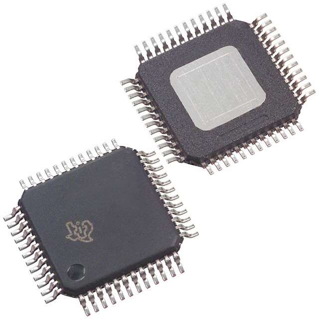


 工商网监
湘ICP备2023018690号
工商网监
湘ICP备2023018690号
