Mosfet
Metal�Oxide�Semiconductor�Field�Effect�Transistor
OptiMOS™�Small-Signal-Transistor,�100V
BSL373SN
Data�Sheet
Rev.�2.0
Final
Industrial�&�Multimarket
�BSL373SN
OptiMOS™ Small-Signal-Transistor
Product Summary
Features
• N-channel
• Enhancement mode
VDS
100
V
RDS(on),max
0.23
Ω
ID
2.0
A
• Avalanche rated
• Qualified according to AEC Q101
• RoHS compliant
TSOP6
• Halogen-free acording to IEC61249-2-21
6
5
4
1
2
3
Type
Package
Tape and Reel Info
Marking
Halogen Free
Packing
BSL373SN
TSOP6
H6327: 3000 pcs/ reel
sPY
Yes
Non dry
Maximum ratings, at T j=25 °C, unless otherwise specified
Parameter
Symbol Conditions
Continuous drain current
ID
Value
T A=25 °C
2.0
T A=70 °C
1.6
Unit
A
Pulsed drain current
I D,pulse
T A=25 °C
8.0
Avalanche energy, single pulse
E AS
I D=2 A, R GS=25 Ω
33
mJ
Reverse diode dv /dt
dv /dt
I D=2 A, V DS=50 V,
di /dt =200 A/µs,
T j,max=150 °C
6
kV/µs
Gate source voltage
V GS
Power dissipation1)
P tot
Operating and storage temperature
T j, T stg
ESD Class
T A=25 °C
JESD22-A114 -HBM
Soldering Temperature
V
2.0
W
-55 ... 150
°C
0 (2|I D|R DS(on)max,
I D=1.6 A
3.35
-
S
1)
Device on 40mm x 40mm x 1.5mm epoxy PCB FR4 with 6cm² (one layer, 70µm thick) copper area for drain
connection. PCB is vertical in still air. (t < 5 sec.)
Rev 2.0
page 2
2014-10-16
�BSL373SN
Parameter
Values
Symbol Conditions
Unit
min.
typ.
max.
-
199
265
-
36
48
Dynamic characteristics2)
Input capacitance
C iss
Output capacitance
C oss
Reverse transfer capacitance
Crss
-
14
21
Turn-on delay time
t d(on)
-
4.7
7.1
Rise time
tr
-
5.9
8.9
Turn-off delay time
t d(off)
-
20.6
30.9
Fall time
tf
-
13.6
20.4
Gate to source charge
Q gs
-
0.8
1.1
Gate to drain charge
Q gd
-
2.7
4.0
Gate charge total
Qg
-
6.2
9.3
Gate p
plateau voltage
g
V plateau
-
4.1
-
V
-
-
2.0
A
-
-
7.9
-
0.8
1.1
V
-
27
41
ns
-
60
90
nC
V GS=0 V, V DS=25 V,
f =1 MHz
V DD=50 V, V GS=10 V,
I D=2 A, R G,ext=6 Ω
pF
ns
Gate Charge Characteristics2)
V DD=50 V, I D=2 A,
V GS=0 to 10 V
nC
Reverse Diode
Diode continous forward current
IS
Diode pulse current
I S,pulse
Diode forward voltage
V SD
Reverse recovery time2)
t rr
Reverse recovery charge2)
Q rr
2)
T A=25 °C
V GS=0 V, I F=2 A,
T j=25 °C
V R=50 V, I F=2 A,
di F/dt =200 A/µs
Defined by design. Not subjected to production test
Rev 2.0
page 3
2014-10-16
�BSL373SN
1 Power dissipation
2 Drain current
P tot=f(T A)
I D=f(T A); V GS≥10 V
2.5
2
2
1.5
1.5
ID [A]
Ptot [W]
2.5
1
1
0.5
0.5
0
0
0
40
80
120
160
0
40
80
TA [°C]
120
160
TA [°C]
3 Safe operating area
4 Max. transient thermal impedance
I D=f(V DS); T A=25 °C; D =0
Z thJA=f(t p)
parameter: t p
parameter: D =t p/T
101
102
1 µs
10 µs
100 µs
0.5
1 ms
100
10 ms
0.2
ZthJA [K/W]
ID [A]
5s
10-1
0.1
101
0.05
0.02
10-2
0.01
single pulse
10-3
100
10-1
100
101
102
103
VDS [V]
Rev 2.0
10-4
10-3
10-2
10-1
100
101
102
tp [s]
page 4
2014-10-16
�BSL373SN
5 Typ. output characteristics
6 Typ. drain-source on resistance
I D=f(V DS); T j=25 °C
R DS(on)=f(I D); T j=25 °C
parameter: V GS
parameter: V GS
8
800
7
10 V
6
700
6V
600
5.5 V
500
RDS(on) [mΩ]
ID [A]
5
4
400
5V
3
300
2
200
5V
5.5 V
6V
10 V
4.5 V
1
100
4V
0
0
0
2
4
6
0
1
2
3
VDS [V]
4
5
6
7
5
6
7
ID [A]
7 Typ. transfer characteristics
8 Typ. forward transconductance
I D=f(V GS); |V DS|>2|I D|R DS(on)max
g fs=f(I D); T j=25 °C
7
6
6
5
5
4
4
ID [A]
gfs [S]
7
3
2
3
2
150 °C
25 °C
1
1
0
0
0
1
2
3
4
5
6
VGS [V]
Rev 2.0
0
1
2
3
4
ID [A]
page 5
2014-10-16
�BSL373SN
9 Drain-source on-state resistance
10 Typ. gate threshold voltage
R DS(on)=f(T j); I D=2 A; V GS=10 V
V GS(th)=f(T j); V DS=VGS; I D=218 µA
parameter: I D
600
5
500
4
max
3
typ
VGS(th) [V]
RDS(on) [mΩ]
400
300
max
200
min
2
typ
1
100
0
0
-60
-20
20
60
100
140
-60
-10
Tj [°C]
40
90
140
Tj [°C]
11 Typ. capacitances
12 Forward characteristics of reverse diode
C =f(V DS); V GS=0 V; f =1 MHz; Tj=25°C
I F=f(V SD)
parameter: T j
103
101
Ciss
25 °C
150 °C
100
IF [A]
C [pF]
102
150 °C, 98%
Coss
101
10-1
Crss
25 °C, 98%
100
10-2
0
10
20
30
40
50
60
70
80
90 100
VDS [V]
Rev 2.0
0
0.2
0.4
0.6
0.8
1
1.2
1.4
VSD [V]
page 6
2014-10-16
�BSL373SN
13 Avalanche characteristics
14 Typ. gate charge
I AS=f(t AV); R GS=25 Ω
V GS=f(Q gate); I D=2 A pulsed
parameter: T j(start)
parameter: V DD
101
50 V
10
9
20 V
80 V
8
7
6
VGS [V]
IAV [A]
25 °C
100 °C
125 °C
100
5
4
3
2
1
0
10-1
100
101
102
0
103
1
2
3
4
5
6
7
Qgate [nC]
tAV [µs]
15 Drain-source breakdown voltage
16 Gate charge waveforms
V BR(DSS)=f(T j); I D=250 µA
120
V GS
116
Qg
112
VBR(DSS) [V]
108
104
100
V g s(th)
96
92
88
Q g (th)
Q sw
84
Q gs
80
-60
-20
20
60
100
140
Q gate
Q gd
180
Tj [°C]
Rev 2.0
page 7
2014-10-16
�BSL373SN
TSOP6
Package Outline:
Note: For symmetric types there is no defined Pin 1 orientation in the reel.
Rev 2.0
page 8
2014-10-16
�BSL373SN
Revision�History
BSL373SN
Revision:�2014-10-22,�Rev.�2.0
Previous Revision
Revision
Date
Subjects (major changes since last revision)
2.0
2014-10-22
Release of final version
We�Listen�to�Your�Comments
Any�information�within�this�document�that�you�feel�is�wrong,�unclear�or�missing�at�all?�Your�feedback�will�help�us�to�continuously
improve�the�quality�of�this�document.�Please�send�your�proposal�(including�a�reference�to�this�document)�to:
erratum@infineon.com
Published�by
Infineon�Technologies�AG
81726�München,�Germany
©�2014�Infineon�Technologies�AG
All�Rights�Reserved.
Legal�Disclaimer
The�information�given�in�this�document�shall�in�no�event�be�regarded�as�a�guarantee�of�conditions�or�characteristics.�With
respect�to�any�examples�or�hints�given�herein,�any�typical�values�stated�herein�and/or�any�information�regarding�the�application
of�the�device,�Infineon�Technologies�hereby�disclaims�any�and�all�warranties�and�liabilities�of�any�kind,�including�without
limitation,�warranties�of�non-infringement�of�intellectual�property�rights�of�any�third�party.
Information
For�further�information�on�technology,�delivery�terms�and�conditions�and�prices�please�contact�your�nearest�Infineon
Technologies�Office�(www.infineon.com).
Warnings
Due�to�technical�requirements,�components�may�contain�dangerous�substances.�For�information�on�the�types�in�question,
please�contact�the�nearest�Infineon�Technologies�Office.
The�Infineon�Technologies�component�described�in�this�Data�Sheet�may�be�used�in�life-support�devices�or�systems�and/or
automotive,�aviation�and�aerospace�applications�or�systems�only�with�the�express�written�approval�of�Infineon�Technologies,�if�a
failure�of�such�components�can�reasonably�be�expected�to�cause�the�failure�of�that�life-support,�automotive,�aviation�and
aerospace�device�or�system�or�to�affect�the�safety�or�effectiveness�of�that�device�or�system.�Life�support�devices�or�systems�are
intended�to�be�implanted�in�the�human�body�or�to�support�and/or�maintain�and�sustain�and/or�protect�human�life.�If�they�fail,�it�is
reasonable�to�assume�that�the�health�of�the�user�or�other�persons�may�be�endangered.
9
Rev.�2.0,��2014-10-22
�
很抱歉,暂时无法提供与“BSL373SNH6327XTSA1”相匹配的价格&库存,您可以联系我们找货
免费人工找货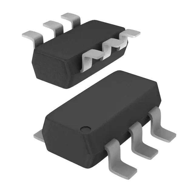


 工商网监
湘ICP备2023018690号
工商网监
湘ICP备2023018690号
